Table of Contents
Advertisement
QQ
3 7 63 1515 0
SERVICE MANUAL
Ver 1.0 2002.02
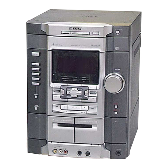
HCD-GX8000/RG77 are the amplifier, CD
player, tape deck and tuner section in
MHC-GX8000/RG77.
TE
L 13942296513
AUDIO POWER SPECIFICATIONS
(HCD-GX8000 only)
POWER OUTPUT AND TOTAL
HARMONIC DISTORTION:
With 6-ohm loads, both channels driven, from
120 Hz - 10 kHz; rates 200 watts per channel
minimum RMS power, with no more than 10%
total harmonic distortion from 250 miliwatts to
rated output.
Amplifier section
HCD-GX8000
Total harmonic distortion
HCD-RG77
The following are measured at AC 120, 220, 240V
50/60 Hz
DIN power output (rated) 160 + 160 watts
Continuous RMS power output (reference)
Inputs
GAME (VIDEO):
(phono jack)
GAME (AUDIO):
(phono jacks)
MD/VIDEO (AUDIO) IN: voltage 450 mV/250 mV,
(phono jacks)
MIC:
(phone jack)
www
.
Sony Corporation
9-873-542-01
2002B0500-1
Home Audio Company
C 2002.02
Published by Sony Engineering Corporation
http://www.xiaoyu163.com
HCD-GX8000/RG77
Outputs
VIDEO OUT:
(phono jacks)
PHONES:
(stereo mini jack)
FRONT SPEAKER:
SURROUND SPEAKER: accepts impedance of
CD player section
System
Laser
Less than 0.1 % (6 ohms
at 1 kHz, 100 W)
Laser Output
(6 ohms at 1 kHz, DIN)
Frequency response
200 + 200 watts
Wave length
(6 ohms at 1 kHz,
CD OPTICAL DIGITAL OUT
10% THD)
(Square optical connector jack, rear panel)
Wave length
1 Vp-p, 75 ohms
Output Level
Voltage 250 mV,
impedance 47 kilohms
Tape player section
Recording system
impedance 47 kilohms
Frequency response
sensitivity 1 mV,
impedance 10 kilohms
x
ao
y
i
http://www.xiaoyu163.com
8
Model Name Using Similar Mechanism
CD Mechanism Type
CD
Section
Base Unit Name
Optical Pick-up Name
Model Name Using Similar Mechanism
TAPE
Q Q
Section
Tape Transport Mechanism Type
3
6 7
1 3
SPECIFICATIONS
max. output level 1 Vp-p,
unbalanced, Sync.
negative load impedance
75 ohms
accepts headphones of
8 ohms or more
accepts impedance of 6 to
16 ohms
24 ohms or more
Compact disc and digital
audio system
Semiconductor laser
(λ=795nm)
Max. 44.6 µW*
*This output is the value
measured at a distance of
200 mm from the
objective lens surface on
the Optical Pick-up Block
with 7 mm aperture.
2 Hz – 20 kHz (±0.5 dB)
795 nm
660 nm
–18 dBm
4-track 2-channel stereo
50 – 13,000 Hz (±3 dB),
using Sony TYPE I
cassette
COMPACT DISC DECK RECEIVER
u163
.
2 9
9 4
2 8
NEW
CDM58E-30BD60C
BU-30BD60C
A-MAX.3
NEW
TCM-230AWR41CS
1 5
0 5
8
2 9
9 4
Tuner section
FM stereo, FM/AM superheterodyne tuner
FM tuner section
Tuning range
Antenna
Antenna terminals
Intermediate frequency
AM tuner section
Tuning range
Latin and North American models:
Middle Eastern models:
Other models:
Antenna
Antenna terminals
Intermediate frequency
– Continued on next page –
m
co
9 9
US Model
HCD-GX8000
E Model
HCD-RG77
2 8
9 9
87.5 – 108.0 MHz
FM lead antenna
75 ohm unbalanced
10.7 MHz
530 – 1,710 kHz
(with the interval set at 10
kHz)
531 – 1,710 kHz
(with the interval set at 9
kHz)
531 – 1,602 kHz
(with the interval set at 9
kHz)
531 – 1,602 kHz
(with the interval set at 9
kHz)
530 – 1,710 kHz
(with the interval set at 10
kHz)
AM loop antenna
External antenna terminal
450 kHz
Advertisement
Table of Contents


Need help?
Do you have a question about the HCD-GX8000 and is the answer not in the manual?
Questions and answers