Table of Contents
Advertisement
Quick Links
Advertisement
Chapters
Table of Contents

Related Manuals for MSI MS-98J4


Summary of Contents for MSI MS-98J4
- Page 1 MS-98J4 (v1.x) Industrial Computer Board...
-
Page 2: Copyright And Trademarks Notice
Preface Copyright and Trademarks Notice Copyright © Micro-Star Int’l Co., Ltd. All rights reserved. The MSI logo used is a registered trademark of Micro-Star Int’l Co., Ltd. All other marks and names mentioned may be trademarks of their respective owners. No warranty as to accuracy or completeness is expressed or implied. -
Page 3: Safety Instructions
MS-98J4 Safety Instructions ■ Always read the safety instructions carefully. ■ Keep this User’s Manual for future reference. ■ Keep this equipment away from humidity. ■ Lay this equipment on a reliable flat surface before setting it up. ■ The openings on the enclosure are for air convection hence protects the equipment from overheating. -
Page 4: Chemical Substances Information
Chemical Substances Information In compliance with chemical substances regulations, such as the EU REACH Regulation (Regulation EC No. 1907/2006 of the European Parliament and the Council), MSI provides the information of chemical substances in products at: https://www.msi.com/html/popup/csr/evmtprtt_pcm.html Battery Information European Union: Batteries, battery packs, and accumulators should not be disposed of as unsorted household waste. -
Page 5: Ce Conformity
MS-98J4 CE Conformity Hereby, Micro-Star International CO., LTD declares that this device is in compliance with the essential safety requirements and other relevant provisions set out in the European Directive. FCC-B Radio Frequency Interference Statement This equipment has been tested and found to comply with the limits for a Class B digital device, pursuant to Part 15 of the FCC Rules. -
Page 6: Table Of Contents
Preface CONTENTS Copyright and Trademarks Notice ..............ii Revision History .................... ii Technical Support ..................ii Safety Instructions ..................iii Chemical Substances Information ............... iv Battery Information ..................iv CE Conformity ....................v FCC-B Radio Frequency Interference Statement ......... v WEEE Statement ..................v 1. -
Page 7: Overview
Overview Thank you for choosing the MS-98J4, an excellent industrial computer board. Based on the innovative Intel Kaby Lake/ Skylake Processor, the MS- ® 98J4 is engineered to provide reliable performance for a wide variety of industrial applications. 1-1-1... -
Page 8: Specifications
Overview Specifications Processor ■ Intel Kaby Lake-U Core™ i7, Core™ i5, Core™ i3 Series Processor ® ■ Intel Skylake-U Core™ i7, Core™ i5, Core™ i3 Series Processor ® ■ Intel Kaby Lake-R Core™ i5 Series Processor ® ■ Integrated with Processor Memory ■... - Page 9 MS-98J4 Graphics ■ Integrated Intel HD Graphics ® ■ 2 * LVDS 18/24 bit, Dual Channel - LVDS1 shared with eDP - LVDS2 shared with DP2/HDMI2.0 - Max resolution 1920x1200@60Hz ■ 1 * eDP - Shared with LVDS1 - Max resolution 4096×2304@60Hz ■...
- Page 10 Overview Internal I/O ■ 1 * DC power connector (Optional) ■ 1 * CPU fan header ■ 1 * System fan header ■ 2 * SATA 6Gb/s ports ■ 2 * SATA power box headers ■ 1 * Vertical USB2.0 connector (1 port) (Optional) ■...
- Page 11 MS-98J4 SKU Comparison SKUs SKU1 SKU2 SKU3 Features Processor Intel Core™ i5-8250U Intel Core™ i5-7300U Intel Core™ i3-6100U ■ eDP/LVDS1 ■ eDP/LVDS1 ■ LVDS1 ■ HDMI2.0/LVDS2 ■ DP2/LVDS2 ■ LVDS2 Display ■ HDMI1.4 ■ DP1 ■ DP1 LVDS Graphics HDMI...
-
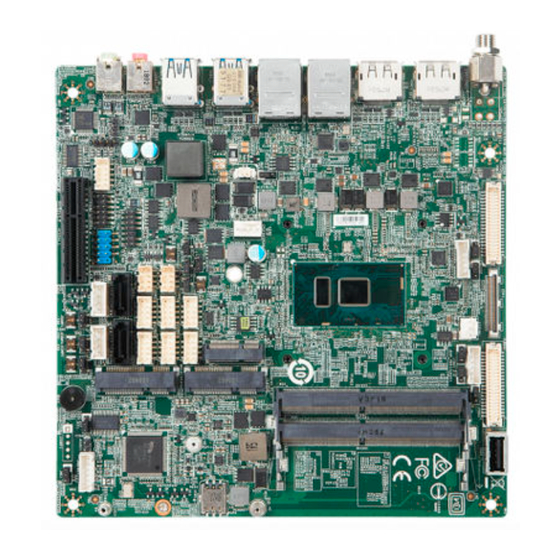
Page 12: Layout
Overview Layout System Fan LVDS2 Inverter eDP Power Power Jumper Jumper LVDS2 LVDS1 LVDS2 LVDS1 LVDS2 Power USB2.0 Inverter Inverter Jumper Rear Panel LVDS1 Power Jumper LVDS1 Inverter Power Jumper DDR4 SO-DIMM CPU Fan Key E CMOS Jumper Nano SIM Power Mini- PCIe Jumper... -
Page 13: Rear Panel I/O Options
MS-98J4 Rear Panel I/O Options SKU1 DC Jack HDMI1.4 HDMI2.0 GbE RJ45 Ports USB3.0 Ports Mic-In Line-Out Port Port Jack Jack SKU2 DC Jack DisplayPort DisplayPort GbE RJ45 Ports USB3.0 Ports Mic-In Line-Out Jack Jack SKU3 DC-In DisplayPort GbE RJ45 Port USB3.0 Ports... -
Page 15: Hardware Setup
Hardware Setup This chapter provides you with the information about hardware setup procedures. While doing the installation, be careful in holding the components and follow the installation procedures. For some components, if you install in the wrong orientation, the components will not work properly. - Page 16 Hardware Setup Components Reference Guide Memory ....................2-3 Power Supply ..................2-4 DC Power Connector: JPWR2 ..............2-4 SATA Power Connector: JSATAPWR1, JSATAPWR2 ........2-4 Rear Panel I/O ...................2-5 Connector ..................2-7 CPU Fan Power Connector: CPUFAN1 .............2-7 System Fan Power Connector: SYSFAN1 ..........2-7 SMBus Connector: JSMB1 ................2-7 USB2.0 Connector: JUSB1, JUSB2, USB2 ..........2-8 Serial ATA Connector: SATA1, SATA2 ............2-8 Front Panel Connector: JFP1 ..............2-9...
-
Page 17: Memory
MS-98J4 Memory The SO-DIMM slot is intended for memory modules. 1. Locate the SO-DIMM slot. Align the notch on the DIMM with the key on the slot and insert the DIMM into the slot. 2. Push the DIMM gently downwards until the slot levers click and lock the DIMM in place. -
Page 18: Power Supply
Hardware Setup Power Supply DC Power Connector: JPWR2 This connector allows you to connect a DC-in power cable. SATA Power Connector: JSATAPWR1, JSATAPWR2 This connector is used to provide power to SATA devices. Important • Make sure all power connectors are connected to the power supply to ensure stable operation of the motherboard. -
Page 19: Rear Panel I/O
MS-98J4 Rear Panel I/O SKU1 DC Jack HDMI1.4 HDMI2.0 GbE RJ45 Ports USB3.0 Ports Mic-In Line-Out Port Port Jack Jack SKU2 DC Jack DisplayPort DisplayPort GbE RJ45 Ports USB3.0 Ports Mic-In Line-Out Jack Jack SKU3 DC-In DisplayPort GbE RJ45 Port USB3.0 Ports... - Page 20 Hardware Setup GbE RJ45 Port The standard single RJ45 LAN jack is provided for connection to the Local Area Network (LAN). You can connect a network cable to it. LED Status Description No link Active Yellow Linked Blinking Data activity Speed LED Active 10 Mbps connection...
-
Page 21: Connector
MS-98J4 Connector CPU Fan Power Connector: CPUFAN1 The fan power connector supports CPU cooling fans with +12V. When connecting the wire to the connectors, always note that the red wire is the positive and should be connected to the +12V; the black wire is Ground and should be connected to GND. -
Page 22: Usb2.0 Connector: Jusb1, Jusb2, Usb2
Hardware Setup USB2.0 Connector: JUSB1, JUSB2, USB2 This connector is ideal for connecting USB devices such as keyboard, mouse, or other USB-compatible devices. Important Note that the pins of VCC and GND must be connected correctly to avoid possible damage. Serial ATA Connector: SATA1, SATA2 This connector is a high-speed Serial ATA interface port. -
Page 23: Front Panel Connector: Jfp1
MS-98J4 Front Panel Connector: JFP1 This front panel connector is provided for electrical connection to the front panel switches & LEDs and is compliant with Intel Front Panel I/O Connectivity Design Guide. PW LED (+) PW LED (-) PW SW (+) -
Page 24: Lvds Inverter Connector: Jinv1, Jinv2
Hardware Setup LVDS Inverter Connector: JINV1, JINV2 The connector is provided for LCD backlight options. LVDS Connector: JLVDS1, JLVDS2 The LVDS (Low Voltage Differential Signal) connector provides a digital interface typically used with flat panels. After connecting the LVDS flat panel, be sure to check the panel datasheet and set the LVDS jumper to proper power voltage. -
Page 25: Com Port Connector: Jcom1 ~ Jcom6
MS-98J4 COM Port Connector: JCOM1 ~ JCOM6 This connector is a 16550A high speed communications port that sends/receives 16 bytes FIFOs. You can attach a serial device to it. JCOM1 and JCOM2 support RS232/422/485. JCOM3 ~ JCOM6 support RS232. JCOM1 ~ JCOM2... -
Page 26: Audio Amplifier Header: Jamp1
Hardware Setup Audio Amplifier Header: JAMP1 The connector is used to connect audio amplifiers to enhance audio performance. S/PDIF Header: JSPD1 This header is used to connect S/PDIF (Sony & Philips Digital Interconnect Format) interface for digital audio transmission. Chassis Intrusion Header: JCASE1 This connector connects to the chassis intrusion switch cable. -
Page 27: Gpio (Dio) Connector: Jgpio1
MS-98J4 GPIO (DIO) Connector: JGPIO1 This connector is provided for the General-Purpose Input/Output (GPIO) peripheral module. eDP Connector: EDP1 This connector is for connecting the flat eDP cable. 2-13... -
Page 28: Jumper
Hardware Setup Jumper Important Avoid adjusting jumpers when the system is on; it will damage the motherboard. Clear CMOS Jumper: JCMOS1 There is a CMOS RAM onboard that has a power supply from an external battery to keep the data of system configuration. With the CMOS RAM, the system can automatically boot OS every time it is turned on. -
Page 29: Jcom1~Jcom2 Power Jumper: Jcomp1, Jcomp2
MS-98J4 JCOM1~JCOM2 Power Jumper: JCOMP1, JCOMP2 These jumpers specify the operation voltage of the JCOM1~JCOM2 serial ports. +12V JCOM3~JCOM6 Power Jumper: JCOMP3 ~ JCOMP6 These jumpers specify the operation voltage of the JCOM3~JCOM6 serial ports. +12V +12V LVDS Power Jumper: JVDD1, JVDD2 Use this jumper to specify the operation voltage of the LVDS interface flat panel. -
Page 30: Slot
Hardware Setup Slot PCIe (Peripheral Component Interconnect Express) Slot The PCI Express slot supports PCIe interface expansion cards (signal shared with M.2 Key M, auto switch by switch IC and PCIe x4 as top priority). PCIe x4 slot M2_M1: M.2 Slot (Key M, 2280) for SSD Please install the M.2 solid-state drive (SSD) into the M.2 slot as shown below. -
Page 31: Mini-Pcie (Peripheral Component Interconnect Express) Slot
MS-98J4 Mini-PCIe (Peripheral Component Interconnect Express) Slot The Mini-PCIe slot is provided for WiFi modules, Bluetooth modules, TV tuner cards and other Mini-PCIe cards. ■ MPCIE/MSATA1 slot supports Mini-PCIe and mSATA cards. ■ MINI_PCIE1 slot supports Mini-PCIe cards. Nano SIM Holder This holder is provided for 3G, 4G, LTE, WiFi, BT, CANBus Nano SIM cards. -
Page 33: Bios Setup
BIOS Setup This chapter provides information on the BIOS Setup program and allows users to configure the system for optimal use. Users may need to run the Setup program when: ■ An error message appears on the screen at system startup and requests users to run SETUP. -
Page 34: Entering Setup
BIOS Setup Entering Setup Power on the computer and the system will start POST (Power On Self Test) process. When the message below appears on the screen, press <DEL> or <F2> key to enter Setup. Press <DEL> or <F2> to enter SETUP If the message disappears before you respond and you still wish to enter Setup, restart the system by turning it OFF and On or pressing the RESET button. - Page 35 MS-98J4 Control Keys ← → Select Screen ↑ ↓ Select Item Enter Select Change Option General Help Previous Values Optimized Defaults Save & Reset Exit Getting Help After entering the Setup menu, the first menu you will see is the Main Menu.
-
Page 36: The Menu Bar
BIOS Setup The Menu Bar ▶ Main Use this menu for basic system configurations, such as time, date, etc. ▶ Advanced Use this menu to set up the items of special enhanced features. ▶ Boot Use this menu to specify the priority of boot devices. ▶... -
Page 37: Main
MS-98J4 Main ▶ System Date This setting allows you to set the system date. The date format is <Day>, <Month> <Date> <Year>. ▶ System Time This setting allows you to set the system time. The time format is <Hour> <Minute> <Second>. -
Page 38: Advanced
BIOS Setup Advanced ▶ Full Screen Logo Display This BIOS feature determines if the BIOS should hide the normal POST messages with the motherboard or system manufacturer’s full-screen logo. When it is enabled, the BIOS will display the full-screen logo during the boot-up sequence, hiding normal POST messages. - Page 39 MS-98J4 ▶ CPU Configuration ▶ Intel Virtualization Technology Virtualization enhanced by Intel Virtualization Technology will allow a platform to run multiple operating systems and applications in independent partitions. With virtualization, one computer system can function as multiple “Virtual” systems. ▶ Active Processor Cores This setting specifies the number of active processor cores.
- Page 40 BIOS Setup ▶ C States This setting controls the C-State (CPU Power state). C-State performance indicates the ability to run the processor in lower power states when the PC is idle. This setting enables/disables the C-State Configuration for power saving purposes.
- Page 41 MS-98J4 ▶ H/W Monitor These items display the current status of all monitored hardware devices/ components such as voltages, temperatures and all fans’ speeds. ▶ Smart Fan Configuration ▶ CPUFAN1, SYSFAN1 This setting enables/disables the Smart Fan function. Smart Fan is an...
- Page 42 BIOS Setup ▶ PCI/PCIE Device Configuration ▶ Legacy USB Support Set to [Enabled] if you need to use any USB 1.1/2.0 device in the operating system that does not support or have any USB 1.1/2.0 driver installed, such as DOS and SCO Unix. ▶...
- Page 43 MS-98J4 ▶ GPIO Group Configuration ▶ GPO0 ~ GPO3 These settings control the operation mode of the specified GPIO. 3-11...
-
Page 44: Boot
BIOS Setup Boot ▶ CSM Support This setting enables/disables the support for Compatibility Support Module, a part of the Intel Platform Innovation Framework for EFI providing the capability to support legacy BIOS interfaces. ▶ Video This setting selects the video mode. ▶... -
Page 45: Security
MS-98J4 Security ▶ Administrator Password Administrator Password controls access to the BIOS Setup utility. ▶ User Password User Password controls access to the system at boot and to the BIOS Setup utility. ▶ Chassis Intrusion The field enables or disables the feature of recording the chassis intrusion status and issuing a warning message if the chassis is once opened. - Page 46 BIOS Setup ▶ PCH-FW Configuration ▶ ME Firmware Version, ME Firmware Mode, ME Firmware SKU, ME File System Integrity Value, ME Firmware Status 1, ME Firmware Status 2, NFC Support These settings show the firmware information of the Intel ME (Management Engine).
- Page 47 MS-98J4 ▶ Firmware Update Configuration ▶ ME FW Image Re-Flash This setting enables/disables the ME FW image reflash. ▶ PTT Configuration Intel Platform Trust Technology (PTT) is a platform functionality for credential storage and key management used by Microsoft Windows.
- Page 48 BIOS Setup ▶ ME Debug Configuration ▶ AMT Configuration Intel Active Management Technology (AMT) is hardware-based technology for remotely managing and securing PCs out-of-band. 3-16...
- Page 49 MS-98J4 ▶ Trusted Computing ▶ Security Device Support This setting enables/disables BIOS support for security device. When set to [Disable], the OS will not show security device. TCG EFI protocol and INT1A interface will not be available. ▶ SHA-1 PCR Bank, SHA256 PCR Bank These settings enable/disable the SHA-1 PCR Bank and SHA256 PCR Bank.
- Page 50 BIOS Setup ▶ Serial Port Console Redirection COM1 ▶ Console Redirection Console Redirection operates in host systems that do not have a monitor and keyboard attached. This setting enables/disables the operation of console redirection. When set to [Enabled], BIOS redirects and sends all contents that should be displayed on the screen to the serial COM port for display on the terminal screen.
- Page 51 MS-98J4 the host system and terminal(s). This setting specifies the type of terminal device for console redirection. ▶ Bits per second, Data Bits, Parity, Stop Bits This setting specifies the transfer rate (bits per second, data bits, parity, stop bits) of Console Redirection.
- Page 52 BIOS Setup ▶ Redirect After POST This setting determines whether or not to keep terminals’ console redirection running after the POST has booted. Serial Port for Out-of-Band Management/ Windows Emergency Management Services (EMS) ▶ Console Redirection Console Redirection operates in host systems that do not have a monitor and keyboard attached.
-
Page 53: Chipset
MS-98J4 Chipset ▶ DVMT Pre-Allocated This setting selects DVMT 5.0 Pre-Allocated (Fixed) Graphics Memory size used by the Internal Graphics Device. ▶ DVMT Total Gfx Mem This setting specifies the memory size for DVMT. ▶ Primary IGFX Boot Display Use the field to select the primary IGFX boot display of the system. -
Page 54: Power
BIOS Setup Power ▶ Restore AC Power Loss This setting specifies whether your system will reboot after a power failure or interrupt occurs. Available settings are: [Power Off] Leaves the computer in the power off state. [Power On] Leaves the computer in the power on state. [Last State] Restores the system to the previous status before power failure or interrupt occurred. - Page 55 MS-98J4 ** Advanced Resume Events Control ** ▶ OnChip GbE/USB This field specifies whether the system will be awakened from power saving modes when activity or input signal of onchip LAN or USB devices is detected. ▶ PCIE PME/Ring This field specifies whether the system will be awakened from power saving modes when activity or input signal of onboard PCIE PME/Ring is detected.
-
Page 56: Save & Exit
BIOS Setup Save & Exit ▶ Save Changes and Reset Save changes to CMOS and reset the system. ▶ Discard Changes and Exit Abandon all changes and exit the Setup Utility. ▶ Discard Changes Abandon all changes. ▶ Load Optimized Defaults Use this menu to load the default values set by the motherboard manufacturer specifically for optimal performance of the motherboard. - Page 57 Appendix GPIO WDT BKL Programming This appendix provides WDT (Watch Dog Timer), GPIO (General Purpose Input/ Output) and LVDS Backlight programming guide. 2-A-1...
- Page 58 GPIO WDT BKL Programming CONTENT Abstract .................... A-3 General Purposed IO ............... A-4 Watchdog Timer ................A-5 LVDS Backlight Brightness Control ..........A-6 SMBus Access ................. A-7...
-
Page 59: Abstract
MS-98J4 Abstract Abstract In this document, code examples based on C programming language are provided for customer interest. Inportb, Outportb, Inportl and Outportl are basic functions used for access IO ports and defined as following. Inportb: Read a single 8‐bit I/O port. Outportb: Write a single byte to an 8‐bit port. Inportl: Reads a single 32‐bit I/O port. Outportl: Write a single long to a 32‐bit port. ... -
Page 60: General Purposed Io
GPIO WDT BKL Programming General Purposed IO 1. General Purposed IO – GPIO/DIO The GPIO port configuration addresses are listed in the following table: Name IO Port IO address Name IO Port IO address N_GPI0 0x22 Bit 4 N_GPO0 0x21 Bit 0 N_GPI1 0x22 Bit 5 N_GPO1 0x21 Bit 1 N_GPI2 0x22 Bit 6 N_GPO2 0x21 Bit 2 N_GPI3 0x22 Bit 7 N_GPO3 0x21 Bit 3 ... -
Page 61: Watchdog Timer
MS-98J4 Watchdog Timer 2. Watchdog Timer – WDT The base address (WDT_BASE) of WDT configuration registers is 0xA10. Set WDT Time Unit val = Inportb (WDT_BASE + 0x05); // Read current WDT setting val = val | 0x08; // minute mode. val = val & 0xF7 if second mode Outportb (WDT_BASE + 0x05, val); // Write back WDT setting Set WDT Time Outportb (WDT_BASE + 0x06, Time); // Write WDT time, value 1 to 255. Enable WDT val = Inportb (WDT_BASE + 0x0A); // Read current WDT_PME setting val = val | 0x01; // Enable WDT OUT: WDOUT_EN (bit 0) set to 1. ... -
Page 62: Lvds Backlight Brightness Control
GPIO WDT BKL Programming LVDS Backlight Brightness Control 3. LVDS Backlight Brightness Control The LVDS controller support 17 level of backlight brightness value from 0 (30%) to 16 (100%) and it is accessible through SMBus. The associated access method (SMBus_ReadByte, SMBus_WriteByte) are provided in part 4. Set the Level of LVDS Backlight 1. Write 0xED into address 0x7F on SMBus device 0x42. 2. - Page 63 MS-98J4 SMBus Access 4. SMBus Access The base address of SMBus must be known before access. The relevant bus and device information are as following. #define IO_SC 0xCF8 #define IO_DA 0xCFC #define PCIBASEADDRESS 0x80000000 #define PCI_BUS_NUM 0 #define PCI_DEV_NUM 31 #define PCI_FUN_NUM ...
Need help?
Do you have a question about the MS-98J4 and is the answer not in the manual?
Questions and answers