Table of Contents
Advertisement
Quick Links
Information furnished by XIA LLC is believed to be accurate and reliable. However, no responsibility is assumed by
XIA LLC for its use, or for any infringements of patents or other rights of third parties which may result from its use.
No license is granted by implication or otherwise under any patent or patent rights of XIA LLC. XIA LLC reserves
the right to change hardware or software specifications at any time without notice.
Pixie-16
User Manual
Version 3.00
August 21, 2018
Hardware Revisions: B, C, D, F
XIA LLC
31057 Genstar Rd
Hayward, CA 94544 USA
Email: support@xia.com
Tel: (510) 401-5760; Fax: (510) 401-5761
http://www.xia.com/
Advertisement
Table of Contents

Subscribe to Our Youtube Channel
Related Manuals for XIA PIXIE-16

Summary of Contents for XIA PIXIE-16
- Page 1 Information furnished by XIA LLC is believed to be accurate and reliable. However, no responsibility is assumed by XIA LLC for its use, or for any infringements of patents or other rights of third parties which may result from its use.
-
Page 2: Table Of Contents
GATE Inputs (Rev. D Modules only) ................. 17 1.5.7 3.3V I/O Connector (Rev. B and C Modules only) ............. 18 1.5.8 Digital Input/output Signals Supported by Standard Firmware (all Pixie-16 revisions) ..19 Front End Attenuation and Termination ..................21 1.6.1 Rev. F Modules ........................21 1.6.2... - Page 3 Baseline Control & Acquire Baselines ................41 3.3.7 Control Registers......................... 41 3.3.8 CFD Trigger ........................45 3.3.8.1 100 MHz and 250 MHz Pixie-16 modules ..............45 3.3.8.2 500 MHz Pixie-16 modules ..................47 3.3.9 Trigger Stretch Lengths ...................... 48 3.3.10 FIFO Delays ........................
- Page 4 PCI and Trigger Interface ......................80 Theory of Operation ..........................81 Digital Filters for Radiation Detectors ..................81 Trapezoidal Filtering in a Pixie-16 Module ................83 Baselines and Preamplifier Decay Times ................... 84 Thresholds and Pileup Inspection ....................85 Filter Range ..........................87 Run Statistics ..........................
-
Page 5: Safety
The Pixie-16 module is powered through a custom made PXI/Compact PCI 6U crate. Please refer to the crate manual for the correct AC voltage connections. The crate must be powered down to insert and remove the module. The Pixie-16 module is not hot swappable! -
Page 6: Warranty Statement
In order to obtain service under this warranty, Customer must notify XIA LLC of the defect before the expiration of the warranty period and make suitable arrangements for the performance of the service. -
Page 7: Manual Conventions
Pixie-16 User Manual August 21, 2018 Manual Conventions The following conventions are used throughout this manual Convention Description Example The sequence The » symbol leads you Run Results»MCA Histogram directs you to through nested menu items » pull down the Run Results menu, and select the and dialog box options. -
Page 8: Introduction
HPGe gamma ray detectors, but has since been applied to an ever broadening range of applications. The DGF Pixie-16 is a 16-channel all-digital waveform acquisition and spectrometer card based on the CompactPCI/PXI standard for fast data readout to the host. It combines spectroscopy with waveform digitizing and the option of on-line pulse shape analysis. -
Page 9: Pixie-16 Features
Pixie-16 User Manual August 21, 2018 1.1 Pixie-16 Features Designed for Segmented germanium detectors, Silicon strip detectors, Arrays of scintillation detectors, Synchronous waveform capture for gamma- ray tracking, Sub-nanosecond timing measurements, Mixed systems with different detector types. Accepts input signals directly from detector preamplifier outputs or scintillator/PMT or SiPM combinations ... -
Page 10: Specifications
Pixie-16 User Manual August 21, 2018 1.2 Specifications Table 1-1 Detailed Specifications of Pixie-16 Front Panel I/O 16 analog signal inputs (SMB). Switchable input impedance and attenuation: 50 Ω or 1 kΩ or 4 kΩ (or according to user specification), 1:4 or 1:1 attenuation Jumper selectable 50 Ω... -
Page 11: System Requirements
Pixie-16 modules in a Pixie-16 crate, and a gamma ray detector with appropriate power supplies. 1.3.1 Pixie-16 Crate The Pixie-16 can be operated in any slot from 2 to 14 of a Pixie-16 crate. Slot 1 is used by the crate controller. 1.3.2 Host Computer The Pixie-16 module communicates with a host computer through a PCI interface. -
Page 12: Drivers And Software
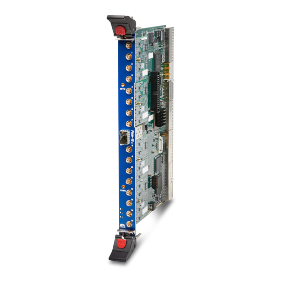
LVDS I/O port, five digital I/O connectors as well as three LEDs near the bottom of the front panel. In addition, a sticker showing Pixie-16 model number (e.g., P16L-250-14, meaning the 14-bit, 250 MHz variant of the Pixie-16) is affixed to the top handle of the Version 3.00... -
Page 13: Analog Signal Input Connectors (All Pixie-16 Revisions)
Clover detector systems. In such systems, each Clover detector has four Revision for a given Pixie-16 module can be determined based on its serial number: S/N 120-134 -> Rev. B; S/N 135-199 -> Rev. C; S/N 200-274 -> Rev. D; S/N 1000 and up -> Rev. F Version 3.00... -
Page 14: Digital I/O Connectors (A, B, C, D, E In Red Color Font) (Rev. F Modules Only)
LVDS format (e.g., using XIA’s LVDS fanout boards), 4 such veto signals can then be input to one Pixie-16 module using the LVDS I/O port. In this way, 4 Compton suppressed Clover detectors (16 HPGe crystal outputs to 16 input channels of the Pixie-16) can be instrumented by one Pixie-16 module. - Page 15 , which are connected to six test output pins on the System FPGA of the Pixie-16, can be used to assist a user in the process of system setup. These test pins are connected to various internal signals of the Pixie-16 to provide insight of the current status of the system.
-
Page 16: Front Panel Leds (All Pixie-16 Revisions)
Pixie-16 module. Instead, it is used to indicate whether or not the External FIFO of the Pixie-16 module is full. It will be ON when there is no more space in the External FIFO for storage of list mode event data, and OFF when there is sufficient space to store at least one more list mode event data. -
Page 17: I/O Connector (Rev. D Modules Only)
J200 Figure 1-5: Pixie-16 Rev. D Module’s 3.3V I/O Connector. On Rev. D Pixie-16 modules, between analog input SMB connectors for channel 7 and channel 8, respectively, is the 3.3V I/O Connector (J200). It has 10 single-ended pins with 2mm spacing. Pins #1, 3, 4, 5, 6, and 8 are connected to six digital output signals from the System FPGA of the Pixie-16 module, i.e. -
Page 18: I/O Connector (Rev. B And C Modules Only)
Figure 1-7: Pixie-16 Rev. B and C Module’s 3.3V I/O Connector. On Rev. B and C Pixie-16 modules, between analog input SMB connectors for channel 11 and channel 12, respectively, is the 3.3V I/O Connector (J100). It has 16 single-ended pins Version 3.00... -
Page 19: Digital Input/Output Signals Supported By Standard Firmware (All Pixie-16 Revisions)
INHIBIT signal is at the logic high level, the run in the Pixie-16 won’t start. Only when the INHIBIT signal goes to the logic low level will the run start in the Pixie-16. During the run, if the INHIBIT signal returns to the logic high level, the run will be aborted. - Page 20 Table 1-11 lists the six Pixie-16 TTL digital output signals. Two groups of six output signals can be chosen through software settings (see Table 3-9, bits [14:12] and [19:16] of TrigConfig0). The last output signal TEST_SEL can be further selected through software settings.
-
Page 21: Front End Attenuation And Termination
August 21, 2018 1.6 Front End Attenuation and Termination Each Pixie-16 module has 16 independent analog input channels. To ensure analog input signal can be properly digitized by each channel’s ADC, the signal must undergo proper signal conditioning including 1) adjusting DC offset of the analog input signal using each channel’s independent Offset DAC and 2) selecting proper input attenuation. -
Page 22: Rev. B, C, D Modules
Figure 1-9 illustrates the input stages of the Rev. B, C, D Pixie-16 modules. Same as the Rev. F modules, they also have a software controlled relay switch. When the relay switch is closed, the input signal is tied to ground via a 50 W resistor, which effectively halves the input signal if it has a 50 W output impedance. -
Page 23: Individual Clock Mode
Pixie-16 master module, which has to be installed in slot 2, other Pixie-16 slave modules can be installed in any other slot of the Pixie-16 crate. In contrast, when the daisy-chained clock mode is used, all Pixie-16 modules have to be installed next to each other, i.e. -
Page 24: Daisy-Chained Clock Mode
Installation of Pixie-16 Modules Multiple Pixie-16 modules can be installed in two 14-slot Pixie-16 crates, #1 and #2. For clock distribution purpose, crate #1 is called the Master crate, where the system-wide global clock for all Pixie-16 modules is... - Page 25 Pixie-16 User Manual August 21, 2018 The Pixie-16 module installed in slot 2 of the Slave crate is called the crate Master module, which is responsible for receiving the global clock from the Master crate and sending such clock to all modules in that crate through length-matched traces on the backplane. The System Director Module is also responsible for sending the global clock to all modules in the Master crate.
- Page 26 A tiny ‘1’ label is painted on the right hand side of the jumpers, indicating pin 1. Figure 1-16 shows the pin ‘1’ in red boxes. Figure 1-16: Pin numbering for the jumpers on the Pixie-16 rear I/O trigger module. Version 3.00...
- Page 27 Pixie-16 User Manual August 21, 2018 Table 1-14 shows the jumper settings of the Pixie-16 rear I/O trigger module #1 in a 2- crate system. Table 1-14 Pixie-16 Rear I/O Trigger Module #1’s Jumper Settings Connect pins 1 and 2 for “P16”...
-
Page 28: Trigger Distribution And Run Synchronization
16 rear I/O trigger modules that are installed in those four separate crates should follow the connection methods shown in Figure 1-17. For the jumper settings on the Pixie-16 rear I/O trigger modules, trigger module #1 and #2 should use the same jumper settings as those in... - Page 29 August 21, 2018 In order to enable the distribution of such global triggers and run synchronization signals, certain Pixie-16 parameters have to be set properly. The parameter that controls the trigger distribution and run synchronization is the Module Control Register B (ModCSRB).
-
Page 30: Installation
2 Installation 2.1 Hardware Setup A Pixie-16 system typically consists of a custom 14-slot 6U PXI crate, one or more Pixie- 16 modules, a crate controller, and accessories. The system is shipped out of the factory in a large wooden box. We recommend proper storage of this wooden box after unpacking, just in case there is a need to return the crate to factory for service or repair (the nails that were used to seal the box are reusable). - Page 31 (example of exposed wires shown in Figure 2-2 bottom), and then connecting the wires to a new plug chosen by the customer. Figure 2-2: An example of the NEMA 5-15 style power plug that come with the Pixie-16 crate and inside look.
-
Page 32: Software Installation In Windows
Connect the detector or preamplifier outputs to the SMB analog inputs of the Pixie-16. SMB-BNC adapter cables are provided by XIA for each module. Make sure to set the input termination appropriately to either 50 Ohm or High-Z by installing or removing, respectively, the jumper on each channel located behind the Pixie-16 front panel before installing the module in the crate. -
Page 33: Software Installation In Linux
Pixie-16 User Manual August 21, 2018 Figure 2-3: Pixie-16 modules shown as “PLX Custom (OEM) PCI 9054 Board” in Windows’ Device Manager. 2.3 Software Installation in Linux The Pixie-16 is fully supported in Linux operating systems. The Pixie-16 software for Linux is built upon two sets of libraries. -
Page 34: Getting Started
2.4 Getting Started This section describes the basic steps to get initial list mode traces or MCA histograms with the Pixie-16 system in a Windows software environment. For detailed introduction to the software interface, refer to section 3. After installation, find the shortcut Pixie16_VB on your desktop and start it with a double click. -
Page 35: Settings
DSP settings for each module (gain, offset, decay times, etc.). The settings are called DSP settings since all DAQ parameters are first downloaded to the DSP on the Pixie-16, and then the DSP will decode the settings and download them to the FPGAs. -
Page 36: Results
Number of FIFO fills in Module 0 (List mode run only). Here each FIFO fill corresponds to approximately 128K list mode data words (32-bit per word). To synchronize data acquisition runs in all Pixie-16 modules, check the option boxes of both “Start/stop runs in all modules simultaneously?” and “Synchronize clocks in all modules?”. -
Page 37: Navigating The Pixie-16 User Interface
3 Navigating the Pixie-16 User Interface 3.1 Overview The Pixie-16 graphical user interface (Figure 2-4) provides a user a simple tool to control the Pixie-16 cards. It was written using Microsoft’s Visual Basic programming language and its underlying function calls are directed to two dynamic link library (DLL) files, Pixie16AppDLL.dll and Pixie16SysDLL.dll. -
Page 38: Settings
In offline mode, the user can still access every button or control of the interface. Results from previous acquisitions can also be viewed by loading the results files. 3.3 Settings The operation of the Pixie-16’s on-board DSP is controlled by a variety of parameters. They can be set using the S DAQ P... -
Page 39: Filter
Pixie-16 User Manual August 21, 2018 3.3.1 Filter The Filter tab shows the settings for the energy filter which measures the pulse height and for the trigger filter which detects pulses. The filtering principle is described in section 6. General rules of thumb for the following important parameters are: 1. -
Page 40: Histogram Control
Pixie-16 uses the decay time to compute and remove the contribution from the exponentially decaying tail of the overlapping prior pulse when computing the pulse height of the current pulse. -
Page 41: Baseline Control & Acquire Baselines
Pixie-16 User Manual August 21, 2018 than the trace length, and for each Pixie-16 variant, there is also a limit for the maximum value of trace delay and trace length. For the 500 MHz Pixie-16 modules, the ADCs are running at 500 MHz, but the traces are recorded with 100 MHz clocks in the FPGA with 5 ADC samples captured in each 10 ns interval. - Page 42 DPM full signal and run synchronization signal generated in the local crate Sort (=1) or do not sort (=0) events from all 16 channels of a Pixie-16 module based on the timestamps of the events, before storing the events in the external FIFO MODCSRB_SORTEVENTS...
- Page 43 (=1: stops taking data when the trace or header DPM for any CCSRA_SYNCDATAACQ channel of any Pixie-16 module in the system is full; =0: stops taking data only when the trace or header DPM for this channel of this Pixie-16 module is full) Choose this channel’s input signal polarity (=1: invert input...
- Page 44 CCSRA_GROUPTRIGSEL = 0, select this channel’s local fast trigger Channel veto signal selection (=1: channel validation trigger from the System FPGA; =0: channel gate input from the Pixie-16 front CCSRA_CHANVETOSEL panel Channel Gate LVDS connector) Module veto signal selection (=1: module validation trigger from the System FPGA;...
-
Page 45: Cfd Trigger
The following CFD algorithm is implemented in the signal processing FPGA of the 100 MHz (Rev. B, C, D and F) and 250 MHz (Rev. F) Pixie-16 modules. Assume the digitized waveform can be represented by data series Trace[i], i = 0, 1, 2, … First the fast filter response (FF) of the digitized waveform is computed as follows: ... - Page 46 Pixie-16 User Manual August 21, 2018 trigger when fast filter crosses over the trigger threshold. The aforementioned CFD parameters correspond to the following DSP parameters. Table 3-3 Corresponding DSP Parameters for the CFD Parameters CFD Parameters DSP Parameters FastLength FastGap...
-
Page 47: 500 Mhz Pixie-16 Modules
B, D, and L. The reason for this is that in the 500 MHz Pixie-16 modules, ADC data that come into the FPGA at the speed of 500 MHz is first slowed down with a ratio of 1:5, in other words, the FPGA captures 5 ADC samples at the rate of 100 MHz, i.e., every 10 ns. -
Page 48: Trigger Stretch Lengths
CFD Parameters Fixed Values for 500 MHz Modules The CFD time given by the 500 MHz Pixie-16 modules consists of two parts: a shift within the 5 ADC samples and a fractional time between two ADC samples where the CFD zero crossing occurred. -
Page 49: Fifo Delays
Fast trigger backplane delay is used to delay the fast trigger pulse before it is sent to the System FPGA for sharing with other modules through the backplane or making coincidence or multiplicity triggers. Table 3-6 Range for Trigger Stretch Lengths and FIFO Delays in Pixie-16 Modules Range Parameters... - Page 50 CHANCSRA[19] = 0: use Channel Veto from front panel ModVeto_sel -- CHANCSRA[20] = 1: use Module Validation Trigger from System FPGA CHANCSRA[20] = 0: use Module Veto from front panel Figure 3-5: Illustration of the signal processing in the Pixie-16 Version 3.00 www.xia.com...
-
Page 51: Multiplicity
Furthermore, up to 16 such groups can be formed within one Pixie-16 module, and each group can have each of its 48 fast trigger signals enabled or disabled by using a user defined contribution mask (48-bit). - Page 52 Pixie-16 User Manual August 21, 2018 can be generated in one Pixie-16 module and they can be used as channel validation triggers, which will be discussed further below. = FastTrigBackplaneEna[15:0] LO[0-15] = FastTrigBackplaneEna[31:16] RO[0-15] RO[0-15] OUT_Right 16 local fast triggers...
- Page 53 SUM of 16 bits SUM >= N 15-1 SUM of 16 bits SUM >= N 15-2 =0,1,…,7 15-0, 15-1, 15-2 = MultMaskHix[24:22] = MultMaskHix[27:25] = MultMaskHix[30:28] x=0,1,2,…,15 SYSTEM FPGA Figure 3-7: Illustration of the Coincidence Trigger in the Pixie-16 Version 3.00 www.xia.com...
- Page 54 Group TrigConfig2[11:8] selects one of the 16 Trigger fast triggers from the right neighbor TrigConfig2[15:12] selects one of the 16 fast triggers from the left neighbor Figure 3-8: Illustration of the Group Trigger in the Pixie-16 Version 3.00 www.xia.com...
-
Page 55: Parameters For Configuring Multiplicity, Coincidence And Group Triggers
16 local fast triggers to its immediate left or right side neighbors. For each Pixie-16 module, there are a total of 16 nearest neighbor bus lines on the backplane to the left side slot, and also a total of 16 nearest neighbor bus lines on the backplane to the right side slot (except for the leftmost slot or rightmost slot in the Pixie- 16 crate). - Page 56 Table 1-11 on the Pixie-16 front panel (see Select source signal for the 6 output of the digital outputs for test/debug purpose on the Pixie-16 [23:20] front panel Select module fast trigger from one of the four sources: Ext_FastTrig_In, FT_LocalCrate_BP,...
- Page 57 Pixie-16 User Manual August 21, 2018 Group trigger #0_2: select one of the 16 fast triggers from the left neighbor based on the value of [11:8] these 4 bits Group trigger #1_0: select one of the 16 fast triggers from the local channels based on the value of...
-
Page 58: Local Fast Trigger Gated By External Fast Trigger
ExtFT_and_LocalFT trigger. FT0 to FT15 are the 16 local fast triggers from the 16 channels of the Pixie-16 module, and the pulse width and delay of each of them can be adjusted using parameters fast trigger backplane length and fast trigger backplane delay, respectively, as discussed in sections 3.3.9 and 3.3.10. - Page 59 Pixie-16 User Manual August 21, 2018 MultMaskHi0[16] = MultMaskHi0[31] = Mult_trig0 Mult_or_Coinc_trig0 Coinc_trig0 ChanTrig0 TrigConfig2[24] = Group Trigger #0 GT_or_EFTandLFT0 ExtFT_and_LocalFT0 MultMaskHi1[16] = MultMaskHi1[31] = Mult_trig1 Mult_or_Coinc_trig1 Coinc_trig1 ChanTrig1 TrigConfig2[24] = Group Trigger #0 GT_or_EFTandLFT1 ExtFT_and_LocalFT1 MultMaskHi2[16] = MultMaskHi2[31] =...
- Page 60 Pixie-16 User Manual August 21, 2018 MultMaskHi8[16] = MultMaskHi8[31] = Mult_trig8 Mult_or_Coinc_trig8 Coinc_trig8 ChanTrig8 TrigConfig2[26] = Group Trigger #2 GT_or_EFTandLFT8 ExtFT_and_LocalFT8 MultMaskHi9[16] = MultMaskHi9[31] = Mult_trig9 Mult_or_Coinc_trig9 Coinc_trig9 ChanTrig9 TrigConfig2[26] = Group Trigger #2 GT_or_EFTandLFT9 ExtFT_and_LocalFT9 MultMaskHi10[16] = MultMaskHi10[31] =...
-
Page 61: Module Validation Trigger
Pixie-16 User Manual August 21, 2018 3.3.11.5 Module Validation Trigger Similar to the channel validation trigger, the module validation trigger can also come from a variety of sources. Figure 3-14 and Figure 3-15 illustrate the four sources for generating the module validation trigger and how to choose each of the four sources. The selections are made through those three parameters ModCSRB, TrigConfig0 and TrigConfig2. - Page 62 ET_LocalCrate_BP in slot #14 ModCSRB[4] = 1: enables one module to send its Ext_ValidTrig_In to all crates through Pixie-16 Rear I/O Trigger Cards installed on the backplane of each crate so that all modules in all crates can receive this trigger signal...
-
Page 63: Module Fast Trigger
Pixie-16 User Manual August 21, 2018 Figure 3-5 shows that the module validation trigger is generated in the System FPGA, and then sent to the Signal Processing FPGA, where it is first latched as a single clock cycle pulse, and then stretched to a pulse whose width is set by the parameter external trigger stretch length. - Page 64 FT_LocalCrate_BP in slot #14 ModCSRB[4] = 1: enables one module to send its Ext_FastTrig_In to all crates through Pixie-16 Rear I/O Trigger Cards installed on the backplane of each crate so that all modules in all crates can receive this trigger signal...
-
Page 65: Qdc
The number of FIFO fills is ignored in MCA runs. To synchronize run start and run stop among all modules in the Pixie-16 system, select the checkbox “Start/stop runs in all modules simultaneously”. All modules will start the data acquisition at the same time;... -
Page 66: Results
Pixie-16 User Manual August 21, 2018 will stop at the same time as well. This avoids the case where events are only partially acquired in different modules. To reset clock counters to zero at the beginning of the run, select the checkbox “Synchronize clocks in all modules”. - Page 67 Pixie-16 User Manual August 21, 2018 Figure 3-20: The Gaussian Fit on a MCA spectrum ROI. On the S panel (Figure 3-21), list mode data such as traces, RACES timestamps, and energy values can be displayed event by event. Figure 3-21: The list mode display panel.
- Page 68 The computations of these filters in the offline mode use the fast filter settings, energy filter settings and CFD settings that are loaded by the Pixie-16 software at boot up. Due to the length of traces that is needed to compute the energy filter sums, the trace length should be long enough to support the offline filter response computations.
- Page 69 Pixie-16 User Manual August 21, 2018 EFRT EFFT EFRT EFRT EFFT EFRT Baseline Energy Net Energy = Energy - Baseline EFRT = Energy Filter Rise Time EFFT = Energy Filter Flat Top To compute energy filter response offline, the ideal settings are: 1.
-
Page 70: Data Acquisition And Data Structures
Pixie-16 module to the host PC. For all Pixie-16 revisions, the list mode data consists of an event header, and a block of trace data if trace recording is enabled for a given channel. The event header contains all... -
Page 71: Output Data Structures
4.2 Output Data Structures 4.2.1 MCA Histogram Data Structure In Pixie-16, each channel is allocated a MCA memory block of 32K words (each word is 32-bit, and K means 1024), for a total MCA memory size of 512K words for the whole module. - Page 72 For Pixie-16 variants with 12-bit ADC’s, the upper 4 bits of each 16-bit ADC data number are filled with 0’s. For Pixie-16 variants with 14-bit ADC’s, the upper 2 bits of each 16-bit ADC data number are filled with 0’s.
- Page 73 8 ns interval, two 4 ns ADC samples are processed in parallel. However, the CFD logic in the 250 MHz Pixie-16 still looks for the CFD zero crossing point at every 4 ns ADC sample. Therefore, when using the 8 ns clock to capture the CFD zero crossing...
-
Page 74: List Mode Data Values
100 MHz, five ADC samples are processed together in parallel. The CFD logic in the 500 MHz Pixie-16 still looks for the CFD zero crossing point at every 2 ns ADC sample. So when using the 10 ns clock to capture the CFD zero crossing point location, there are five possibilities of the CFD zero crossing, i.e., it could occur at each of the 2 ns ADC sample... -
Page 75: List Mode Energy
4.2.3.1.3 Rev. F (12 or 14-bit, 500 MHz) In 500 MHz Pixie-16 modules, as discussed in section 3.3.8.2, the FPGA processes 5 ADC samples at a time with the 100 MHz clock, and the 48-bit timestamp is counted in 100 MHz clock ticks, i.e., 10 ns intervals. -
Page 76: List Mode Trace Length
ADC sampling interval. For instance, a 5 s trace length for a channel in the 500 MHz Pixie-16 is equal to a trace length of 2500 in ADC clock ticks. The 2500 is the number reported in the event header as the trace length. -
Page 77: List Mode External Clock Timestamps
The Pixie-16 settings file (.set) contains the values of DSP parameters that are downloaded to the onboard DSP when a Pixie-16 is booted up. In addition, at the end of each run, either MCA run or list mode run, a settings file will be automatically generated together with either the MCA spectra file (.mca and .asc) or the list mode data file (.bin) and stored in... -
Page 78: Hardware Description
ADC. The anti-aliasing filter, cuts off sharply at the Nyquist frequency, namely half the ADC sampling frequency. Though the Pixie-16 can work with many different signal forms, best performance is to be expected when sending the output from a charge integrating preamplifier or photodetectors (e.g., photomultiplier tubes) directly to the Pixie-16 without any further shaping. -
Page 79: Pulse Processing
Therefore, the FPGA on the Pixie-16 processes the data stream at either 100 or 125 MHz. For 250 MHz variants each channel's 16 (or 14) bit data stream is “de-serialized”... -
Page 80: Pci And Trigger Interface
Broadcom, Inc.) together with an FPGA. The configuration of this PCI IC is stored in a PROM, which is placed in the only DIP-8 IC-socket on the Pixie-16 board. The interface conforms to the commercial PCI standard. It moves 32-bit data words at a time. -
Page 81: Theory Of Operation
Pixie-16 User Manual August 21, 2018 6 Theory of Operation 6.1 Digital Filters for Radiation Detectors Energy dispersive detectors, which include such solid state detectors as Si(Li), HPGe, , CdTe and CZT detectors, are generally operated with charge sensitive preamplifiers as shown in Figure 6-1 (a). - Page 82 Pixie-16 User Manual August 21, 2018 it from the value of the average over the points after the step. That is, as shown in Figure 6-2, averages are computed over the two regions marked “Length” (the “Gap” region is omitted because the signal is changing rapidly here), and their difference taken as a measure of V .
-
Page 83: Trapezoidal Filtering In A Pixie-16 Module
From this point onward, only trapezoidal filtering will be considered as it is implemented in a Pixie-16 module according to Equation 6-2. The result of applying such a filter with Length L=1s and Gap G=0.4s to a -ray event is shown in Figure 6-3. The filter output is clearly trapezoidal in shape and has a rise time equal to L, a flattop equal to G, and a symmetrical fall time equal to L. -
Page 84: Baselines And Preamplifier Decay Times
Pixie-16 User Manual August 21, 2018 ADC output Filter Output 33x10 2L+G 10.0 10.5 11.0 11.5 12.0 12.5µs Time Figure 6-3: Trapezoidal filtering of a preamplifier step with L=1µs and G=0.4µs. 6.3 Baselines and Preamplifier Decay Times Figure 6-4 shows an event over a longer time interval and how the filter treats the preamplifier noise in regions when no -ray pulses are present. -
Page 85: Thresholds And Pileup Inspection
All that is required is to take the filter sums, reconstruct the energy V , and add it to the spectrum. In the Pixie-16, the filter sums are continuously updated in the FPGA (see section 5.2), and are captured into event buffers. Reconstructing the energy and incrementing the spectrum is done by the DSP, so that the FPGA is ready to take new data immediately (unless the buffers are full). - Page 86 ADC Output Fast Filter Output Slow Filter Output Sampling Time Arrival Time Threshold 48µs Time Figure 6-5: Peak detection and sampling in a Pixie-16 module. 36x10 ADC Output Slow Filter Output Fast Filter Output PeakSep 68µs Time Figure 6-6: A sequence of 3 -ray pulses separated by various intervals to show the origin of pileup and demonstrate how it is detected by the Pixie module.
-
Page 87: Filter Range
Table 6-1 and Table 6-2. Table 6-1 Filter clock decimations and filter time granularity for 100 MHz or 500 MHz Pixie-16 Modules Filter range Filter granularity max. -
Page 88: Run Statistics
FASTPEAKS counter is cleared at the start of each run. CHANEVENTS The number of events processed by the DSP for each channel of a Pixie-16 module is called CHANEVENTS. It only counts the events that are actually recorded either into the list mode output data stream or the MCA spectrum. -
Page 89: Count Rates
Pixie-16 User Manual August 21, 2018 6.6.2 Count Rates Count rates are computed in the Pixie-16 C library as follows: FASTPEAKS ICR (6-4) LIVE TIME CHANEVENTS OCR (6-5) TIME Version 3.00 www.xia.com...
Need help?
Do you have a question about the PIXIE-16 and is the answer not in the manual?
Questions and answers