Table of Contents
Advertisement
Quick Links
SERVICE MANUAL
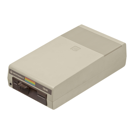
MODEL 1540/1541
DISK DRIVE
NOVEMBER, 1985 PN-314002-01
Commodore Business Machines, Inc.
1200 Wilson Drive, West Chester, Pennsylvania 19380
Commodore makes no expressed or
implied warranties with regard to
the information contained herein.
The information is made available
solely on as is basis, and the entire
risk as to quality and accuracy is
within the user. Commodore shall
not be liable for any consequential
or incidental damages in connection
with the use of the information
contained herein. The listing of any
available replacement part herein
does not constitute in any case a
recommendation,
guaranty as to quality or suitability
of
such
Reproduction
expressed permission, of editorial or
pictorial content, in any matter is
prohibited.
This manual contains copyrighted and proprietary information. No
part of this publication may be reproduced, stored in a retrieval
system, or transmitted in any form by any means, electronic,
mechanical, photocopying, recording or otherwise, without the
prior written permission of Commodore Electronics Limited.
Copyright © 1985 by Commodore Electronics Limited.
All rights reserved.
U.S.A
warranty
or
replacement
part.
or
use
without
Advertisement
Table of Contents

Related Manuals for Commodore 1540


Summary of Contents for Commodore 1540
- Page 1 Commodore Electronics Limited. Copyright © 1985 by Commodore Electronics Limited. All rights reserved.
-
Page 2: Table Of Contents
CONTENTS SPECIFICATIONS • BLOCK DIAGRAM • CARE AND MAINTENANCE • OVERVIEW • FLASH CODE • CIRCUIT THEORY • POWER SUPPLY RESET LOGIC CLOCK CIRCUITS MICROPROCESSOR CONTROL OF RAM AND ROM SERIAL INTERFACE MICROPROCESSOR R/W AND MOTOR CONTROL LOGIC READ/WRITE CONTROL LOGIC READ AMPLIFIER WRITE AMPLIFIER POWER UP/DOWN WRITE PROTECTION... - Page 3 UPGRADE NOTES SCHEMATIC PC ASSEMBLY 250442, 250446 • BOARD LAYOUT PARTS LIST IC PINOUTS AND INTERNAL DIAGRAMS SCHEMATIC POWER SUPPLY ASSEMBLY 154002 • PARTS LIST TRANSFORMER ASSEMBLY DRAWING ALPS DRIVE ASSEMBLY • PARTS LIST WIRING DIAGRAM AND LAYOUT MOTOR CONTROL PCB SCHEMATIC NEWTRONICS DRIVE ASSEMBLY •...
- Page 4 5-1/4 Inch floppy disk. Single sided, single density, soft sectored (double MEDIA density can be used, but not needed) Commodore serial interface INPUT/OUTPUT Second serial port for chaining a second drive or printer MOS 6502 microprocessor - 1 MHz clock...
-
Page 6: Care And Maintenance
Do not touch the exposed area of a diskette. DIAGNOSTIC and ADJUSTMENT procedures are outlined in detail on the diagnostic disk • (Commodore Part #31405101). A manual has been added to the diagnostic package. It contain descriptions of testing procedures and adjustment methods. -
Page 7: Overview
OVERVIEW The drive itself an independent memory device. THe drive is composed of a media clamp rotating mechanism, a head positioning mechanism and an eject mechanism. All positioning operations, excluding insertion and removal of diskettes, are controlled by the internal guide mechanism. Closing the front door causes the media clamp mechanism to operate. - Page 8 1541 CIRCUIT THEORY All circuit diagrams have been taken from the short board schematic 1540049 unless otherwise noted. The short board use a 6116 RAM which replaces the four 2114 I.C.s on the long board. See page 11 for the Read/Write logic differences. The Power Supply The input AC voltage is controlled by switch 1 (SW1).
- Page 9 1541 CIRCUIT THEORY The Reset Circuit The output of the exclusive 'or' gate UD3 pin 6 will be "low" until C46 has charged through R25. Once the voltage across C46 reaches 2 volts, the output of UD3 pin 6 will go "high". This occurs when the disk is powered on, or a reset pulse is generated by a device connected to the serial bus.
- Page 10 1541 CIRCUIT THEORY The Clock Circuits Crystal Y1 outputs a 16Mhz clock signal. THis is input to UD5 on pin 8. UD5 is configured as a ÷ 16 frequency divider. The output of UD5 pin 12 is a 1 MHz clock signal used as the system clock (Phase 0) for the microprocessor.
-
Page 11: Microprocessor Control Of Ram And Rom
1541 CIRCUIT THEORY Microprocessor Control of RAM and ROM UB3 and UB4 are 8192 x 8 bit ROMS that store the Disk Operating System (DOS). UB3 resides at memory locations $C000-$DFFF. UB4 resides at memory locations $E000-$FFFF. UC5 and UC6 decodes the addresses output from the microprocessor when selecting these ROMS. - Page 12 1541 CIRCUIT THEORY The Serial Interface UC3 is a 6522 Versatile Interface Adapter (VIA). Two parallel ports, handshake control, programmable timers, and interrupt control are standard features of the VIA. Port B signals (PB0-PB7) control the serial interface driver ICs (UB1 and UA1). CLK and DATA signals are bidirectional signals connected to pins 4 and 5 of P2 and P3.
-
Page 13: Microprocessor R/W And Motor Control Logic
1541 CIRCUIT THEORY Microprocessor R/W and Motor Control Logic UC2 is a VIA also. During a write operation the microprocessor passes the data to be recorded to Port A of UC2. The data is then loaded into the PLA parallel port (YB0-YB7). The PLA contains a shift register which converts the parallel data into serial data. -
Page 14: Read/Write Control Logic
1541 CIRCUIT THEORY The circuit shown here is from the long board schematic 1540008. This logic was integrated in the PLA (Programmable Logic Array) on the short boards. Read/Write Control Logic During a write operation, UD3 converts parallel data into serial data. The output on pin 9 is input to 'NAND' gate UF5 pin 4. -
Page 15: Read Amplifier
1541 CIRCUIT THEORY Read Amplifier Circuits When data is recorded on the disk, a "1" bit is represented on the disk by a change in direction of magnetic flux, caused by a change in direction of current passed through the R/W coil in the R/W head. When a "0" bit is to be recorded, no change in current flow direction occurs, causing the direction of the magnetic flux to remain the same on the disk. -
Page 16: Write Amplifier
1541 CIRCUIT THEORY Write Amplifier Circuits During a write operation, B must be "high". This forward biases Q7 and CR14. If _B goes "low", Q3 and Q6 become forward biased. If Q goes "low", Q5 and CR15 become forward biased, passing current flow through R/W 1. -
Page 17: Power Up/Down Write Protection
1541 CIRCUIT THEORY Power Up/Down Write Protection This circuit prevents erroneous data from being written on the disk during power up/down sequences. During a power up, the 12VDC supply is not applied to the R/W coils and amplifier circuits before the processor has control of the logic. -
Page 18: Spindle Motor Control Circuits
1541 CIRCUIT THEORY Spindle Motor Control Circuits _MTR output from the PLA is active "low". This signal is passed, through the current driver UD2, to the motor control PCB. When _MTR is "low," Q1 is biased off, and Q2, Q3, and Q4 are biased on, allowing current flow through the spindle motor coil. -
Page 19: Troubleshooting Guide
TROUBLESHOOTING GUIDE NOTE: Always check for latest ROM/ECO upgrade. If socketed IC is suspected bad, be to check socket with ohmmeter. SYMPTOM POSSIBLE SOLUTION No LED's on power up. Is Power cord plugged into wall outlet correctly? Is Power cord plugged in the disk drive correctly? Check line fuse. - Page 20 TROUBLESHOOTING GUIDE (continued) SYMPTOM POSSIBLE SOLUTION Fails to format disk. Check components related to connector P7. Check 6522s. Check the logic array. Stepper Motor does not step forward. Check 6502, 6522s, logic array. Drive speed will not stabilize. Check DC motor. Will not save when the drive Check 6502 microprocessor.
-
Page 21: Resistance Checks
RESISTANCE CHECKS 32 ohms end to centertap 64 ohms end to end Motor coil = 17 ohms Tach coil = 175 ohms at rest Tach coil = 135 - 190 ohms in motion R/W end to end = 32.4 ohms R/w end to centertap = 16.3 ohms Erase coil end to end... -
Page 22: Casework/Accessory Parts List
C 1540052-00 POWER CORD ASSEMBLY C 903508-04 6 PIN DIN CABLE C 1515001-01 USER'S MANUAL C 1540031-03 DEMO DISKETTE C 1540024-01 NOTE: All 1540 Disk Drives were manufactured prior to any changes to the board and used the Alps drive exclusively. - Page 23 Newtronics has a "flipper" type door. DEVICE NUMBER CHANGE The 1540 and 1541 drives are shipped from the factory se for device # 8. The channel can be hardware altered to # 9, 10, or 11 by two methods: 1) Refer to appropriate board layout drawing for the location of the pads provided for this purpose.
- Page 29 UPGRADE NOTES PCB Assembly #1540048 (Schematic 1540049) requires an upgrade to the reset circuit. The upgrade consists of: 1) COMPONENT CHANGES: R25 Change To 6.8K ohm, 1/4 W, +/-5% R57 Add 220 ohm, 1/4 W, +/-5% R58 Add 2K ohm, 1/4 W, +/-5% 2) CUT circuit trace near UA1 (See diagram) 3) INSTALL JUMPER WIRES:...
- Page 32 1540/1541 POWER SUPPLY ASSEMBLY PARTS LIST FUSE HOLDER 903614-01 ROCKER SWITCH 904509-01 POWER CNNCT FILTER 903467-03 sub: 325552-01 FUSE, SLOW BLO, 250V, 1.0A 903556-16 POWER TRANSFORMER 1540009-02...
- Page 33 POWER SUPPLY #1540002...
- Page 34 PARTS LIST 32551901 Alps Drive (Black) 32551902 Alps Drive (Brown) 31410001 ALP DOOR/HUB ASSEMBLY Door Assy w/Spring Hub/Collet Assy Arm Support Assy 41310101 ALP LEFT DISK GUIDE ASSEMBLY Diskette guide LED Assy w/Harness Write Protect Assy 31410201 ALP RIGHT DISK GUIDE 31410301 ALP FRONT BEZEL (Black) 31410302 ALP FRONT BEZEL (Brown) 31410401 ALP R/W HEAD ASSEMBLY...
- Page 35 Eject Spring 31411201 ALP HARDWARE Assorted Screws Zero Stop Tab 3147401 UNV Replacement Load Pad...
- Page 36 ALPS DRIVE ASSEMBLIES 1540/1541...
- Page 37 SYMBOL DESCRIPTION I.C. Sony CX-065B Transistor 2SC2785 Transistor 2SC2785 Transistor 2SA1175 Transistor B703-Q36E CR1,2,3,4,5 Diode IN4148 R1,7 Resistor, 1 kOhm, 1/4W Resistor, 68 kOhm, 1/4W Resistor, 220 Ohm, 1/4W Resistor, 3.3 kOhm, 1/4W Resistor, 2.7 kOhm, 1/4W Resistor, 820 Ohm, 1/4W Resistor, 150 Ohm, 1/4W Resistor, 0.68 Ohm, 2W Resistor, 5.1 kOhm, 1/8W...
Need help?
Do you have a question about the 1540 and is the answer not in the manual?
Questions and answers