Table of Contents
Advertisement
Quick Links
TABLE OF CONTENTS
1 Safety Precautions----------------------------------------------- 3
1.1. General Guidelines---------------------------------------- 3
1.2. Before Repair and Adjustment ------------------------- 4
1.3. Caution For Fuse Replacement------------------------ 4
1.4. Protection Circuitry ---------------------------------------- 4
1.5. Safety Part Information----------------------------------- 4
2 Warning -------------------------------------------------------------- 6
to Electrostatically Sensitive (ES) Devices---------- 6
2.2. Precaution of Laser Diode------------------------------- 7
3 Service Navigation ----------------------------------------------- 9
3.1. Service Information --------------------------------------- 9
4 Specifications ----------------------------------------------------10
5 Location of Controls and Components ------------------11
5.1. Main Unit Key Button Operations--------------------- 11
5.2. Remote Control Key Button Operations ------------12
6 Operating Instructions-----------------------------------------13
Model No.
Product Color: (S)...Silver Type
PAGE
6.1. Disc and MP3 Information ----------------------------- 13
7 Self diagnosis and special mode setting --------------- 14
7.1. Service Mode Summary Table------------------------ 14
7.2. Service Mode Table ------------------------------------- 15
7.3. Error Code Table ----------------------------------------- 18
8 Troubleshooting Guide --------------------------------------- 19
8.1. CD Door Unit Jam--------------------------------------- 19
9 Disassembly and Assembly Instructions--------------- 21
9.1. Disassembly flow chart --------------------------------- 22
9.2. Type of Screw--------------------------------------------- 23
9.3. Main Parts Location Diagram ------------------------- 23
9.4. Disassembly of CD Door Unit------------------------- 24
9.5. Disassembly of Net Frame Assembly--------------- 26
9.6. Disassembly of Top Ornament------------------------ 28
9.7. Disassembly of Bottom Ornament ------------------- 29
9.8. Disassembly of Speaker Unit (SP1) ----------------- 30
9.9. Disassembly of Speaker Unit (SP2) ----------------- 31
9.10. Disassembly of Panel 1 & Panel 2 P.C.B. --------- 33
© Panasonic Corporation 2009. All rights reserved.
Unauthorized copying and distribution is a violation of
law.
Compact Stereo System
SC-HC4GK
SC-HC4GT
PSG0907003CE
PAGE
Advertisement
Table of Contents

Related Manuals for Panasonic SC-HC4GK


Summary of Contents for Panasonic SC-HC4GK
-
Page 1: Table Of Contents
5.2. Remote Control Key Button Operations ------------12 9.9. Disassembly of Speaker Unit (SP2) ----------------- 31 6 Operating Instructions-----------------------------------------13 9.10. Disassembly of Panel 1 & Panel 2 P.C.B. --------- 33 © Panasonic Corporation 2009. All rights reserved. Unauthorized copying and distribution is a violation of law. - Page 2 9.11. Disassembly of Front Panel Block ------------------- 35 17.5. MAIN CIRCUIT (4/4) ----------------------------------- 102 9.12. Disassembly of Tuner Pack --------------------------- 35 17.6. FL CIRCUIT, PANEL 1 CIRCUIT and PANEL 9.13. Disassembly of SMPS Unit ---------------------------- 36 2 CIRCUIT------------------------------------------------ 103 9.14. Disassembly of AC IN P.C.B.-------------------------- 37 17.7.
-
Page 3: Safety Precautions
1 Safety Precautions 1.1. General Guidelines 1. When servicing, observe the original lead dress. If a short circuit is found, replace all parts which have been overheated or damaged by the short circuit. 2. After servicing, see to it that all the protective devices such as insulation barriers, insulation papers shields are properly installed. -
Page 4: Before Repair And Adjustment
1.2. Before Repair and Adjustment Disconnect AC power, discharge unit AC Capacitors as such C702, C710, C725, C727, C728, C730 and C736 through a 10W, 1W resistor to ground. Caution : DO NOT SHORT-CIRCUIT DIRECTLY (with a screwdriver blade, for instance), as this may destroy solid state devices. After repairs are completed, restore power gradually using a variac, to avoid overcurrent. - Page 5 Safety Ref. No. Part No. Part Name & Description Remarks T581 G4D1A0000117 SWITCHING TRANSFORMER T701 G4DYA0000139 MAIN TRANSFORMER T701 G4DYA0000155 MAIN TRANSFORMER T751 ETS19AB221AG SUB TRANSFORMER Z752 ERZV10V511CS Z752 ERZVA5Z471 PC701 B3PBA0000454 PHOTO COUPLER PC751 B3PBA0000454 PHOTO COUPLER RY701 K6B1AEA00017 RELAY F751 K5D162BK0005...
-
Page 6: Warning
2 Warning 2.1. Prevention of Electro Static Discharge (ESD) to Electrostatically Sensi- tive (ES) Devices Some semiconductor (solid state) devices can be damaged easily by static electricity. Such components commonly are called Elec- trostatically Sensitive (ES) Devices. Examples of typical ES devices are integrated circuits and some field-effect transistors and semiconductor “chip”... -
Page 7: Precaution Of Laser Diode
2.2. Precaution of Laser Diode CAUTION! THIS PRODUCT UTILIZES A LASER. USE OF CONTROLS OR ADJUSTMENTS OR PERFORMANCE OF PROCEDURES OTHER THAN THOSE SPECIFIED HEREIN MAY RESULT IN HAZARDOUS RADIATION EXPOSURE. Caution: This product utilizes a laser diode with the unit turned "on", invisible laser radiation is emitted from the pickup lens. Wavelength: 795 nm (CD) Maximum output radiation power from pickup: 100 μW/VDE Laser radiation from the pickup unit is safety level, but be sure the followings:... -
Page 8: Service Caution Based On Legal Restrictions
2.3. Service caution based on Legal restrictions 2.3.1. General description about Lead Free Solder (PbF) The lead free solder has been used in the mounting process of all electrical components on the printed circuit boards used for this equipment in considering the globally environmental conservation. The normal solder is the alloy of tin (Sn) and lead (Pb). -
Page 9: Service Navigation
3 Service Navigation 3.1. Service Information This service manual contains technical information which will allow service personnel’s to understand and service this model. Please place orders using the parts list and not the drawing reference numbers. If the circuit is changed or modified, this information will be followed by supplement service manual to be filed with original service manual. -
Page 10: Specifications
4 Specifications Operating humidity range 35% to 80 % RH (no condensa- tion) Power consumption in standby mode 0.08 W (approx) (For GT) Power consumption in standby mode 0.2 W (approx) (For GK) Amplifier Section Notes : RMS Output Power Stereo Mode 1. -
Page 11: Location Of Controls And Components
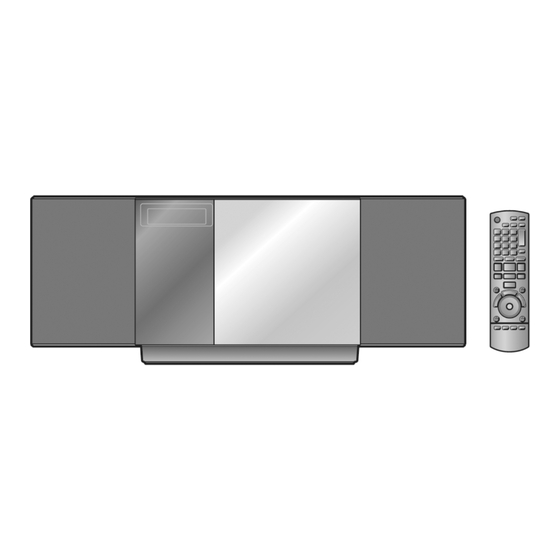
5 Location of Controls and Components 5.1. Main Unit Key Button Operations... -
Page 12: Remote Control Key Button Operations
5.2. Remote Control Key Button Operations... -
Page 13: Operating Instructions
6 Operating Instructions 6.1. Disc and MP3 Information... -
Page 14: Self Diagnosis And Special Mode Setting
7 Self diagnosis and special mode setting This unit is equipped with features of self-diagnostic & special mode setting for checking the functions & reliability. 7.1. Service Mode Summary Table The service modes can be activated by pressing various button combination on the main unit and remote control unit. Below is the summary for the various modes for checking: Player buttons Remote control unit buttons... -
Page 15: Service Mode Table
7.2. Service Mode Table Below is the various special modes for checking:- 7.2.1. Service Mode Table 1 Item FL Display Key Operation Mode Name Description Front Key Self -Diagnostic Mode To enter into self diagnostic 1. Select [ ] for CD mode checking for main unit. - Page 16 7.2.2. Service Mode Table 2 Item FL Display Key Operation Mode Name Description Front Key FL Display Test To check the FL segments In Doctor Mode: display (All segments will 1. Press [1] button on remote con- light up) trol. To cancel, press [0] button on remote control.
- Page 17 Item FL Display Key Operation Mode Name Description Front Key Mecha Sliding Panel To check the operation of In Doctor Mode: Reliability sliding Panel. 1. Press [ ] follow by [2] & then Sequence as follow : [1] button on remote control. 1.
-
Page 18: Error Code Table
7.3. Error Code Table Self-Diagnosis Function provides information on any problems occuring for the unit and its respective components by displaying error codes. Thesed error code such as U**, H** and F** are stored in memory and held unless it is cleared. The error code is automatically display after entering into self-diagnostic mode. -
Page 19: Troubleshooting Guide
8 Troubleshooting Guide 8.1. CD Door Unit Jam 8.1.1. Removing the CD Step 2 : Push the CD Door Unit as arrow shown until the CD is fully in sight. Step 3 : Remove the CD. Step 1 : Insert a flathead screwdriver into the hole behind the CD Door Unit and push the gear fixture from point A to B. - Page 20 8.1.2. Removing the iPod Step 2 : Push the CD Door Unit as arrow shown until the iPod is fully in sight. Step 3 : Remove the iPod. Step 1 : Insert a flathead screwdriver into the hole behind the CD Door Unit and push the gear fixture from point B to A.
-
Page 21: Disassembly And Assembly Instructions
9 Disassembly and Assembly Instructions “ATTENTION SERVICER” Be careful when disassembling and servicing. Some chassis components may have sharp edges Special Note: 1. This section describes the disassembly procedures for all the major printed circuit boards and main components. 2. Before the disassembly process was carried out, do take special note that all safety precautions are to be carried out. (Ensure that no AC power supply is connected during disassembling.) 3. -
Page 22: Disassembly Flow Chart
9.1. Disassembly flow chart The following chart is the procedure for disassembling the casing and inside parts for internal inspection when carrying out the ser- vicing. To assemble the unit, reverse the steps shown in the chart below. -
Page 23: Type Of Screw
9.2. Type of Screw 9.3. Main Parts Location Diagram... -
Page 24: Disassembly Of Cd Door Unit
9.4. Disassembly of CD Door Unit Step 3 : Lift up the CD Door Unit slightly as arrow shown and push it as arrow shown. Step 4 : Remove the CD Door Unit. Caution : Avoid touching the lens during assembling / Dis- assembly of the CD Door Unit. - Page 25 • Assembly of CD Door Unit Caution : Avoid touching the lens during assembling / Dis- assembly of the CD Door Unit. Step 1 : Adjust the gear fixture as diagram shown. Step 2 : Align the CD Door Unit with the (upper & lower rib), guide reel (A &...
-
Page 26: Disassembly Of Net Frame Assembly
9.5. Disassembly Frame Assembly • Disassembly of Net Frame Asembly (L) Caution : During assembly ensure that the bosses are aligned to their respective holes in Front Speaker Assem- Step 1 : Gently lift up Net Frame Assembly (L). bly (L) as shown. Caution : During assembly ensure the net frame assembly (L) is seated properly Step 2 : Remove Net Frame Assembly (L) as arrow shown. - Page 27 • Disassembly of Net Frame Asembly (R) Caution : During assembly ensure that the bosses are aligned to their respective holes in Front Speaker Assem- Step 3 : Gently lift up Net Frame Assembly (R). bly (R) as shown. Step 4 : Remove Net Frame Assembly (R) as arrow shown.
-
Page 28: Disassembly Of Top Ornament
9.6. Disassembly of Top Ornament • Follow the (Step 1) - (Step 4) of item 9.5. Step 3 : Lift up the Top Ornament Unit. Caution : Avoid pulling when detaching the Top Ornament or apply strong force it may lead to the broken of connect- Step 1 : Remove 4 screws. -
Page 29: Disassembly Of Bottom Ornament
9.7. Disassembly of Bottom Orna- ment • Follow the (Step 1) - (Step 4) of item 9.5. Step 3 : Remove the Bottom Ornament. Step 1 : Remove 4 screws. Step 2 : Gently release the 4 catches on the Bottom Ornament. Caution : Take extra care not to damage the Bottom Orna- ment during disassembling. -
Page 30: Disassembly Of Speaker Unit (Sp1)
9.8. Disassembly of Speaker Unit (SP1) • Follow the (Step 1) - (Step 4) of item 9.5. • Follow the (Step 1) - (Step 3) of item 9.6. • Follow the (Step 1) - (Step 3) of item 9.7. Step 3 : Place the Front Speaker Assembly (L) on a support block as shown. -
Page 31: Disassembly Of Speaker Unit (Sp2)
9.9. Disassembly of Speaker Unit (SP2) • Follow the (Step 1) - (Step 4) of item 9.5. • Follow the (Step 1) - (Step 3) of item 9.6. • Follow the (Step 1) - (Step 3) of item 9.7. Step 4 : Remove 4 screws. Step 1 : Remove 5 scews. - Page 32 Step 4 : Remove 4 screws. Step 3 : Place the Front Speaker Assembly (R) on a support block as shown. Step 5 : Desolder the speaker terminals of the red (+) and black (-) speaker wires. Step 6 : Remove Speaker unit (SP2). Caution : During assembling of the Front Speaker Assem- bly (R), insert the speaker wires into the hole in the Front Speaker Assembly (R).
-
Page 33: Disassembly Of Panel 1 & Panel 2 P.c.b
9.10. Disassembly of Panel 1 & Panel 2 P.C.B. • Follow the (Step 1) - (Step 4) of item 9.4. • Follow the (Step 1) - (Step 4) of item 9.5. • Follow the (Step 1) - (Step 3) of item 9.6. •... - Page 34 Step 5 : Press to release catches to lift up the Front Panel P.C.B.. Block slightly as arrow shown. Step 9 : Lift up the himelon. Step 10 : Remove Top Ornament Unit. Step 11 : Remove 6 screws. Step 6 : Lift up the Front Panel Block. Step 12 : Remove Panel 1 P.C.B.
-
Page 35: Disassembly Of Front Panel Block
9.11. Disassembly of Front Panel 9.12. Disassembly of Tuner Pack Block • Follow the (Step 1) - (Step 4) of item 9.4. • Follow the (Step 1) - (Step 4) of item 9.5. • Follow the (Step 1) - (Step 4) of item 9.4. •... -
Page 36: Disassembly Of Smps Unit
9.13. Disassembly of SMPS Unit • Follow the (Step 1) - (Step 4) of item 9.4. • Follow the (Step 1) - (Step 4) of item 9.5. • Follow the (Step 1) - (Step 3) of item 9.6. • Follow the (Step 1) - (Step 3) of item 9.7. •... -
Page 37: Disassembly Of Ac In P.c.b
9.14. Disassembly of AC IN P.C.B. • Follow the (Step 1) - (Step 4) of item 9.4. • Follow the (Step 1) - (Step 4) of item 9.5. • Follow the (Step 1) - (Step 3) of item 9.6. • Follow the (Step 1) - (Step 3) of item 9.7. •... - Page 38 Step 3 : Remove 3 screws. Step 6 : Remove 1 screw. Step 7 : Remove Support 2 P.C.B.. Step 4 : Flip over SMPS Barrier A. Step 8 : Using flathead screwdriver to release catch. Step 5 : Remove 1 screw.
-
Page 39: Disassembly Of Smps P.c.b
9.15. Disassembly of SMPS P.C.B. • Follow the (Step 1) - (Step 4) of item 9.4. • Follow the (Step 1) - (Step 4) of item 9.5. • Follow the (Step 1) - (Step 3) of item 9.6. • Follow the (Step 1) - (Step 3) of item 9.7. •... -
Page 40: Replacement Of Switching Regulator Ic (Ic702)
9.16. Replacement of Switching Reg- ulator IC (IC702) • Follow the (Step 1) - (Step 4) of item 9.4. • Follow the (Step 1) - (Step 4) of item 9.5. • Follow the (Step 1) - (Step 3) of item 9.6. •... - Page 41 • Assembly of Switching Regulator IC (IC702) Step 2 : Remove 1 screw. Step 1 : Install Switching Regulator IC (IC702) onto SMPS Step 3 : Remove Switching Regulator IC (IC702). P.C.B.. Step 2 : Fix the Switching Regulator IC (IC702) onto the heat- sink unit with 1 screw.
-
Page 42: Replacement Of Diode (D702)
9.17. Replacement of Diode (D702) • Follow the (Step 1) - (Step 4) of item 9.4. • Follow the (Step 1) - (Step 4) of item 9.5. • Follow the (Step 1) - (Step 3) of item 9.6. • Follow the (Step 1) - (Step 3) of item 9.7. •... - Page 43 • Assembly of Diode (D702) Step 2 : Remove 1 screw. Step 3 : Remove Diode (D702). Step 1 : Install Diode (D702) onto SMPS P.C.B.. Step 2 : Fix the Diode (D702) onto the heatsink unit with 1 screw. Caution : Ensure the pins are inserted &...
-
Page 44: Replacement Of Diode (D704)
9.18. Replacement of Diode (D704) • Follow the (Step 1) - (Step 4) of item 9.4. • Follow the (Step 1) - (Step 4) of item 9.5. • Follow the (Step 1) - (Step 3) of item 9.6. • Follow the (Step 1) - (Step 3) of item 9.7. •... - Page 45 • Assembly of Diode (D704) Step 1 : Fix the Diode (D704) onto the heatsink unit with 1 screw. Caution : Ensure the Diode (D704) is tightly screwed to the heatsink unit. Step 3 : Remove the heatsink unit with Diode (D704) as arrow shown.
-
Page 46: Disassembly Of Main P.c.b
9.19. Disassembly of Main P.C.B. • Follow the (Step 1) - (Step 4) of item 9.4. • Follow the (Step 1) - (Step 4) of item 9.5. • Follow the (Step 1) - (Step 3) of item 9.6. • Follow the (Step 1) - (Step 3) of item 9.7. •... - Page 47 Step 4 : Detach 22P FFC cable at the connector (CN806) on Step 6 : Detach 2P cable at the connector (CN804) on the Main the Main P.C.B.. P.C.B.. Step 7 : Detach 3P cable at the connector (CN653) on the Main P.C.B..
- Page 48 Step 10 : Detach 12P cable at the connector (CN110) on the Main P.C.B.. Step 11 : Flip over the Main P.C.B. as arrow shown. Caution : Ensure that all wires are properly dressed as shown during assembling of the Main P.C.B.. Step 12 : Detach 14P FFC cable at the connector (CN381) on the Main P.C.B..
-
Page 49: Disassembly Of Fan
9.20. Disassembly of Fan 9.21. Disassembly of AUX / HP P.C.B. • Follow the (Step 1) - (Step 4) of item 9.4. • Follow the (Step 1) - (Step 4) of item 9.5. • Follow the (Step 1) - (Step 4) of item 9.4. •... -
Page 50: Disassembly Of Traverse Deck
9.22. Disassembly of Traverse Deck • Follow the (Step 1) - (Step 4) of item 9.4. • Follow the (Step 1) - (Step 4) of item 9.5. • Follow the (Step 1) - (Step 3) of item 9.6. • Follow the (Step 1) - (Step 3) of item 9.7. •... -
Page 51: Disassembly Of Traverse Cover & Traverse Unit
9.23. Disassembly of Traverse Cover & Traverse Unit • Follow the (Step 1) - (Step 4) of item 9.4. • Follow the (Step 1) - (Step 4) of item 9.5. • Follow the (Step 1) - (Step 3) of item 9.6. •... -
Page 52: Disassembly Of Cd Servo P.c.b
9.24. Disassembly Servo P.C.B. • Follow the (Step 1) - (Step 4) of item 9.4. • Follow the (Step 1) - (Step 4) of item 9.5. • Follow the (Step 1) - (Step 3) of item 9.6. • Follow the (Step 1) - (Step 3) of item 9.7. •... -
Page 53: Disassembly Of D-Amp P.c.b
9.25. Disassembly of D-Amp P.C.B. 9.26. Disassembly of Fan Unit (iPod) • Follow the (Step 1) - (Step 4) of item 9.4. • Follow the (Step 1) - (Step 4) of item 9.4. • Follow the (Step 1) - (Step 4) of item 9.5. •... - Page 54 Step 2 : Remove the support 1 P.C.B.. Step 4 : Remove the Fan Unit (iPod). Caution : During assembling ensure the fan unit (iPod) is seated properly. Step 3 : Remove the silicon plate.
-
Page 55: Disassembly Of Usb Module Assembly
9.27. Disassembly of USB Module 9.28. Disassembly of USB P.C.B. Assembly • Follow the (Step 1) - (Step 4) of item 9.4. • Follow the (Step 1) - (Step 4) of item 9.5. • Follow the (Step 1) - (Step 4) of item 9.4. •... -
Page 56: Disassembly Of Sd Lid
9.29. Disassembly of SD Lid • Follow the (Step 1) - (Step 4) of item 9.4. • Follow the (Step 1) - (Step 4) of item 9.5. • Follow the (Step 1) - (Step 3) of item 9.6. • Follow the (Step 1) - (Step 3) of item 9.7. •... -
Page 57: Disassembly Of Fl P.c.b
9.30. Disassembly of FL P.C.B. • Follow the (Step 1) - (Step 4) of item 9.4. • Follow the (Step 1) - (Step 4) of item 9.5. • Follow the (Step 1) - (Step 3) of item 9.6. • Follow the (Step 1) - (Step 3) of item 9.7. •... -
Page 58: Disassembly Of Ipod P.c.b
9.31. Disassembly of iPod P.C.B. • Follow the (Step 1) - (Step 4) of item 9.4. • Follow the (Step 1) - (Step 4) of item 9.5. • Follow the (Step 1) - (Step 3) of item 9.6. • Follow the (Step 1) - (Step 3) of item 9.7. •... - Page 59 Step 4 : Press and hold the docking holder with gentle force as Step 6 : Remove 2 screws. arrows shown to remove the docking holder as arrow shown. Step 7 : Release the 2 catches on the iPod Assembly. Step 5 : Remove the iPod Docking Tub Assembly.
- Page 60 • Assembly of Docking Holder Step 9 : Remove the iPod P.C.B. as arrow shown. Step 1 : Place the docking holder underneath the catch. Caution : Using the 2 locaters as guides, ensure that the docking holder is properly located. Step 2 : Align the docking holder to the 2 bosses on the front panel block.
-
Page 61: Disassembly Of Motor P.c.b
9.32. Disassembly of Motor P.C.B. • Follow the (Step 1) - (Step 4) of item 9.4. • Follow the (Step 1) - (Step 4) of item 9.5. • Follow the (Step 1) - (Step 3) of item 9.6. • Follow the (Step 1) - (Step 3) of item 9.7. •... -
Page 62: Disassembly Of Position Sw P.c.b
9.33. Disassembly of Position SW P.C.B. • Follow the (Step 1) - (Step 4) of item 9.4. • Follow the (Step 1) - (Step 4) of item 9.5. • Follow the (Step 1) - (Step 3) of item 9.6. • Follow the (Step 1) - (Step 3) of item 9.7. •... -
Page 63: Disassembly Of Ipod Sw P.c.b
9.34. Disassembly of iPod SW P.C.B. • Follow the (Step 1) - (Step 4) of item 9.4. • Follow the (Step 1) - (Step 4) of item 9.5. • Follow the (Step 1) - (Step 3) of item 9.6. • Follow the (Step 1) - (Step 3) of item 9.7. •... -
Page 64: Disassembly Of Ir P.c.b
9.35. Disassembly of IR P.C.B. • Follow the (Step 1) - (Step 4) of item 9.4. • Follow the (Step 1) - (Step 4) of item 9.5. • Follow the (Step 1) - (Step 3) of item 9.6. • Follow the (Step 1) - (Step 3) of item 9.7. •... - Page 65 Caution : During assembly of the IR P.C.B., connect 3P cable to the connector (CN652) on the Main P.C.B. and dress the cable as shown.
-
Page 66: Service Position
10 Service Position Note: For description of the disassembly procedures, see the Section 9 10.1. Checking and Repairing Main P.C.B. • Checking & Repairing Main P.C.B. (Side A) Step 1 : Remove CD Door Unit. Step 2 : Remove Net Frame. Step 3 : Remove Top Ornament. - Page 67 • Checking & Repairing Main P.C.B. (Side B) Step 15 : Lift up the Main P.C.B. slightly to detach 8P cable at the connector (CN902). Step 11 : Remove 7 screw. Step 16 : Detach 2P cable at the connector (CN2815) on the Main P.C.B..
- Page 68 Step 19 : Detach 22P FFC cable at the connector (CN806) on the Main P.C.B.. Step 23 : Remove the silicon plate. Step 24 : Remove the Fan Unit (iPod). Step 20 : Flip over the Main P.C.B. as arrow shown and place it on an insulation sheet.
- Page 69 Step 27 : Flip over the D-Amp P.C.B. as arrow shown. Step 25 : Remove the Fan Assembly. Step 28 : Remove 2 screws. Step 26 : Remove 3 screws.
- Page 70 Step 29 : Remove USB Module Assembly. Caution : Take extra care not to damage the ground wire that is connected from the Jupiter Module to the Main P.C.B. during disassembling. Step 32 : Desolder pins as diagram shown. Step 30 : Remove 2 screws. Step 31 : Remove SD Holder.
- Page 71 Step 34 : Remove the D-Amp insulator. Step 36 : Remove the FL P.C.B.. Step 35 : Release the catch on the FL P.C.B.. Step 37 : Connect 12P cable at the connector (CN110) on the Main P.C.B..
- Page 72 Step 38 : Connect 22P FFC cable at the connector (CN806) on the Main P.C.B.. Step 40 : Connect 2P cable at the connector (CN2815) on the Main P.C.B.. Step 41 : Connect 3P cable at the connector (CN653) on the Main P.C.B..
-
Page 73: Checking And Repairing D-Amp P.c.b
10.2. Checking and Repairing D- Main P.C.B.. Amp P.C.B. • Follow the (Step 1) - (Step 43) of item 10.1. Step 43 : Connect 4P cable at the connector (CN2) on the D- Amp P.C.B.. Step 1 : Check and repair D-Amp P.C.B. according to the dia- Step 44 : Check and repair Main P.C.B. -
Page 74: Checking And Repairing Fl P.c.b
10.3. Checking and Repairing FL 10.4. Checking and Repairing CD P.C.B. Servo P.C.B. • Follow the (Step 1) - (Step 43) of item 10.1. • Follow the (Step 1) - (Step 43) of item 10.1. Step 1 : Check and repair FL P.C.B. according to the diagram Step 1 : Check and repair CD Servo P.C.B. -
Page 75: Checking And Repairing Usb P.c.b
10.5. Checking and Repairing USB 10.6. Checking and Repairing AC IN P.C.B. P.C.B. • Follow the (Step 1) - (Step 43) of item 10.1. Step 1 : Remove CD Door Unit. Step 2 : Remove Net Frame. Step 3 : Remove Top Ornament. Step 4 : Remove Bottom Ornament. - Page 76 Step 9 : Lift up the himelon. Step 10 : Remove 1 screw. Step 12 : Remove 3 screws. Step11 : Lift up 2 pieces of himelon. Step 13 : Flip over SMPS Unit as arrow shown. Step 14 : Lift up 2 pieces of himelon.
- Page 77 Step 18 : Remove AC IN P.C.B.. Step 15 : Remove 1 screw. Step 16 : Remove Support 2 P.C.B.. Step 17 : Using flathead screwdriver to release catch. Step 19 : Connect 4P cable at the connector (CN2).
-
Page 78: Checking And Repairing Smps P.c.b
10.7. Checking and Repairing SMPS P.C.B. • Follow the (Step 1) - (Step 20) of item 10.6. Step 20 : Lay the AC IN P.C.B. on an insulation sheet. Step 21 : Check and repair AC IN P.C.B. according to the dia- gram shown. - Page 79 Step 3 : Connect the ground wire on the Main P.C.B. to the SMPS shield using a ground extension as shown. Step 4 : Check and repair SMPS P.C.B. according to the dia- gram shown.
-
Page 80: Voltage Measurement & Waveform Chart
STANDBY Ref No. IC7002 MODE CD PLAY STANDBY Ref No. IC7002 MODE CD PLAY STANDBY Ref No. IC7003 MODE CD PLAY STANDBY Ref No. IC7003 MODE CD PLAY STANDBY Ref No. Q7601 MODE CD PLAY STANDBY SC-HC4GK/GT CD SERVO P.C.B. -
Page 81: D-Amp P.c.b
17.0 17.0 24.6 17.0 STANDBY Ref No. MODE CD PLAY STANDBY Ref No. MODE CD PLAY STANDBY SC-HC4GK/GT D-AMP P.C.B. 11.3. FL P.C.B. Ref No. IC6801 MODE -25.5 -25.5 -23.3 -14.6 -18.9 -14.5 -25.5 CD PLAY STANDBY Ref No. IC6801... -
Page 82: Main P.c.b. (1/3)
IC504 MODE CD PLAY 15.2 STANDBY 15.2 Ref No. IC505 MODE CD PLAY 15.0 STANDBY 15.2 Ref No. IC551 MODE CD PLAY STANDBY Ref No. IC601 MODE CD PLAY STANDBY Ref No. IC650 MODE CD PLAY STANDBY SC-HC4GK/GT MAIN P.C.B. -
Page 83: Main P.c.b. (2/3)
CD PLAY 13.3 14.9 13.8 14.8 14.8 STANDBY -0.1 Ref No. Q251 Q252 Q253 Q302 Q382 MODE CD PLAY -2.6 -2.6 -2.6 -0.3 STANDBY Ref No. Q451 Q452 Q453 Q509 Q511 MODE CD PLAY -2.6 -2.5 -2.5 STANDBY SC-HC4GK/GT MAIN P.C.B. -
Page 84: Main P.c.b. (3/3)
Ref No. QR514 QR515 QR554 QR804 QR805 MODE CD PLAY STANDBY Ref No. QR806 MODE CD PLAY STANDBY SC-HC4GK/GT MAIN P.C.B. 11.7. SMPS P.C.B. Ref No. IC701 MODE CD PLAY 13.6 STANDBY Ref No. IC702 MODE CD PLAY -1.1 -3.5 -5.0... -
Page 85: Usb P.c.b
11.8. USB P.C.B. IC900 REF NO. MODE CD PLAY STANDBY IC900 REF NO. MODE CD PLAY STANDBY IC900 REF NO. MODE CD PLAY STANDBY IC900 REF NO. MODE CD PLAY STANDBY SC-HC4GK/GT USB P.C.B. -
Page 86: Waveform Chart
11.9. Waveform Chart WF No. IC1 - 1,44 WF No. IC1 - 9,10 WF No. IC1 - 13,14 WF No. IC1 - 31,32 (PLAY) (PLAY) (PLAY) (PLAY) 120mVp-p (2.5usec.div) 22.4Vp-p (1usec.div) 22.4Vp-p (1usec.div) 22.2Vp-p (1usec.div) WF No. IC1 - 35,36 WF No. - Page 87 WF No. IC900 - 11 WF No. IC900 - 12 WF No. IC7001 - 56,59 WF No. IC7001 - 80 (PLAY) (PLAY) (PLAY) (PLAY) 1.62Vp-p (50nsec.div) 2.68Vp-p (50nsec.div) 800mVp-p (10msec.div) 2.72Vp-p (50nsec.div) WF No. IC7001 - 81 (PLAY) 2Vp-p (10usec.div)
-
Page 88: Illustration Of Ic's, Transistors And Diodes
12 Illustration of IC’s, Transistors and Diodes C1AB00003012 (44P) C0CBCBD00008 C1AB00003013 (52P) C0DAAMH00015 B0ADCJ000020 C0ABBB000230 (8P) C0CBCBC00090 C0HBB0000057 (44P) C0DAAMH00013 MN6627954AMA (100P) MNZSFB5KJM2 (64P) RFKWMAHC4EP (100P) No.1 No.1 C0GAE0000007 C0DBAYH00005 C0AABB000085 BA5948FPE2 (28P) MIP2F20MSSCF C3ABMB000050 (26P) C0EBE0000482 C0DAEMZ00001 C0CBADD00010 B1ABCF000176 B1ABGC000005 B1BAAJ000003 C0EBJ0000336... -
Page 89: Overall Simplified Block
13 Overall Simplified Block Digital Amp. ASP IC APF FILTER GAIN TRE / MID / BASS Sound Mode & Dynamic Bass Pre AMP VOL2 Vcc: +17.1 SMPS Micro-p 1 Line FL SMPS Vcc: Display Back up +17.1... - Page 90 D_D0WFIC/D_MPUTX/D_MPURX/D_MPUCLK/ DAB L &R SELECTOR D_MPUMOD/D_NRST/D_PLLSDA/ D-PLLSCL/D_NRFRST/DAB_PON VOL 1 HEADPHONE TUNER L &R TRE/MID/BASS TUNER PACK MPORT IPOD L &R SOUND ENHANCER & TU_ST/TU_SD/ TU_SDA/TU_SCLK CD L &R SD L &R/ MUX RDS SD_LIN/SD_RIN AUDIO SIGNAL PROCESSOR I²C (D_MPUTX/ D_MPUCLK0 DIGITAL AMP BLOCK MUTE LEFT...
- Page 91 Vp / FL / Gnd iPod TUNER Power Amplifier +9V DC-DC Main Pre AMP SMPS +7.5V CD LID MOTOR +5.5V Standby SMPS MCU SYS 3.3V +3.9V Photo LID SW Remote IR...
-
Page 92: Block Diagram
[23]TRVP TRAVERSE [CH2] LEVEL <+3.3V> SHIFT OPTICAL PICKUP P.C.B MOTOR A0~A10 A0~A10 12~15 IC7003 C3ABMB000050 16MB DRAM 83~86 M7302* [21]SPOUT SPINDLE [CH1] LEVEL SHIFT MOTOR D0~D3 DQ1~DQ4 MUTE [22]PC [CH1] MUTE [CH2] CD SERVO P.C.B SC-HC4GK/GT CD SERVO BLOCK DIAGRAM... -
Page 93: Main (1/2) / Tuner / Ipod / Fl / Motor / Usb Block Diagram
FL P.C.B DC DETECT iPod [12]OSCO [13]OSCI [15]XI [16]XO CN1002 CN381 SWITCH TO MAIN (2/2) CN1002 CN381 BLOCK DIAGRAM X802 X801 <iPod5V> 8MHz 32KHz iPod P.C.B SC-HC4GK/GT MAIN (1/2) / TUNER / iPod / FL / MOTOR / USB BLOCK DIAGRAM... -
Page 94: Main (2/2) / D-Amp Block Diagram
FAN MOTOR DRIVE FAN MOTOR DRIVE [18]WARNING DC DETECT GNDP1 DIODE [19]ERR QR554 TO MAIN (1/2) CN110 PCONT2 PCONT [21]SHUTDOWN BLOCK DIAGRAM SWITCH PDET1 FAN LOCK DETECT CN110 F_SHIFT LEVEL [25]ROSC SHIFTER D-AMP P.C.B SC-HC4GK/GT MAIN (2/2) / D-AMP BLOCK DIAGRAM... -
Page 95: Panel1/2 / Aux/Hp / Ir / Smps / Ac In Block Diagram
IR921 (REMOTE SENSOR) IR P.C.B JK951 MUSIC PORT CN902 CN951 TO MAIN (1/2) CN902 CN951 BLOCK DIAGRAM CN902 CN951 CN902 CN951 CN902 CN951 CN902 CN951 AUX/HP P.C.B SC-HC4GK/GT PANEL1/2 / AUX/HP / IR / SMPS / AC IN BLOCK DIAGRAM... -
Page 96: Wiring Connection Diagram
15 Wiring Connection Diagram MOTOR P.C.B. AUX/HP P.C.B. (Side A) PANEL 2 P.C.B. SOLDER SIDE PANEL 1 P.C.B. (Side A) SOLDER SIDE SOLDER SIDE SOLDER SIDE P903 HEADPHONE USB P.C.B. MT602* USB PORT JK952 JK951 P901* P903* MOTOR P904* SOLDER SIDE 1 . -
Page 97: Schematic Diagram Notes
16 Schematic Diagram Notes (All schematic diagrams may be modified at any time with • Voltage and Signal lines: the development of new technology) : +B Signal Line Notes: : -B Signal Line S641: LEFT switch. S642: CENTER switch. : CD Audio Input Signal Line S643: RIGHT switch. -
Page 98: Schematic Diagram
C7334 STAT 10V220 R7254 REST SW R7323 R7331 C7166 3.3K 0.01 LOADING R7325 R7315 3.3K IC7002 C7164 S7201 REST SW BA5948FPE2 R7335 4CH DRIVER R7332 M7301* M7302* TRAVERSE MOTOR SPINDLE MOTOR IC7003 C7401 C3ABMB000050 16MB DRAM SC-HC4GK/GT CD SERVO CIRCUIT... -
Page 99: Main Circuit (1/4)
R886 100K HP_SW MUTING HP_SW R833 100K C876 1000P C826 0.01 R832 100K C815 680P VSS ON/OFF IC803 IC802 C816 R957 C0EBE0000482 C0CBCBD00008 680P RESET VOLTAGE REGULATOR SYS5V C828 C827 6.3V100 16V10 SYS5VGND TO MAIN SECTION (3/4) SC-HC4GK/GT MAIN CIRCUIT... -
Page 100: Main Circuit (2/4)
VREF- IN SCHEMATIC VREF- DIAGRAM - 7 CN803 PWR_LED PWR_LED 7.5V TO MAIN PANEL 1 CIRCUIT VLED_7.5V SECTION (1/4) KEY1 KEY1 (P901*) KEY2 IN SCHEMATIC KEY2 R898 R899 DIAGRAM - 6 VREF- STBY3.3V TO MAIN SECTION (4/4) SC-HC4GK/GT MAIN CIRCUIT... -
Page 101: Main Circuit (3/4)
USB_IRQ USB_IRQ USB_SDATA USB_SDA DGND CD_CLK DGND CD_STAT USB CIRCUIT CD_DATA (P901) DGND IN SCHEMATIC STCLK DIAGRAM - 11 TERR TERR STREQ STIN CD_MLD CD_RST TO MAIN USB_RST USB_RST SECTION (4/4) DGND DGND D3.3V D3.3V MMOD MMOD SC-HC4GK/GT MAIN CIRCUIT... -
Page 102: Main Circuit (4/4)
SWITCH C454 B1ABCF000176 R451 100P R131 1.2K MUTING CONTROL Q105 Q103 R134 SWITCH B1ABCF000176 B1ABCF000176 MUTING CONTROL MUTING CONTROL SWITCH SWITCH TO MAIN C120 R128 SECTION (3/4) D103 MA2J7280GL D102 D101-D102 MA2J1110GL C119 D101 R130 0.22 4.7M SC-HC4GK/GT MAIN CIRCUIT... -
Page 103: Fl Circuit, Panel 1 Circuit And Panel 2 Circuit
KEY11 1.2K 1.5K 2.2K 3.3K 4.7K IN SCHEMATIC KEY2 KEY21 KEY21 DIAGRAM - 3 VREFGND VREFGND VREFGND S913 S914 S916 S911 S912 S915 D.BASS REV SKIP FWD SKIP STOP/-DEMO VOL- VOL+ SC-HC4GK/GT FL / PANEL 1 / PANEL 2 CIRCUIT... -
Page 104: Tuner Circuit, Aux/Hp Circuit, Ir Circuit, Motor Circuit, Position Sw Circuit And Ipod Sw Circuit
POSITION3 (CN804) VREF- IN SCHEMATIC DIAGRAM - 3 S642 P641* CENTER POSITION1 MAIN CIRCUIT POSITION2 (CN651) POSITION3 IN SCHEMATIC VREF- DIAGRAM - 3 S643 RIGHT SC-HC4GK/GT TUNER / AUX/HP / IR / MOTOR / POSITION SW / iPod SW CIRCUIT... -
Page 105: Ipod Circuit And Ac In Circuit
ERZV10V511CS...GK SMPS CIRCUIT AC IN R727 IN SCHEMATIC JW752A* ZA751 ZA752 4.7M 110V 60Hz...GT DIAGRAM - 10 220V 50Hz...GK FOR GK ONLY C730 F1BAF1020020 1000P SMPS CIRCUIT JW753A* (JW753B*) IN SCHEMATIC DIAGRAM - 10 SC-HC4GK/GT iPod / AC IN CIRCUIT... -
Page 106: D-Amp Circuit
OUT2N G0C150MA0056 VCCP1N VCCP2N VCCP1N VCCP2N POWERDET2 BSP1N BSP2N B1GBCFJJ0051 DC DETECT MA2J1110GL WARNING VHOLD 100K 100K MA2J1110GL 3.9K B1GBCFJJ0051 MUTEX ROSC MUTING CONTROL MUTE_C SHUT DOWN B1GBCFJJ0051 PCONT_2 PCONT SWITCH 15.5V F_SHIFT B1GBCFJJ0051 LEVEL SHIFTER 15.5VGND SC-HC4GK/GT D-AMP CIRCUIT... -
Page 107: Smps Circuit
AC IN CIRCUIT JW753B* (JW753A*) IC751 IN SCHEMATIC MIP2F20MSSCF SWITCHING REGULATOR DIAGRAM - 8 C756 PC751 B3PBA0000454 IC752 FEED BACK K9...GT C758 C0DAEMZ00001 C757 R754 R753 1000P SHUNT REGULATOR R756 R758 R759 R760 R755 470K K10...GK 2.2K R757 ZJ701 SC-HC4GK/GT SMPS CIRCUIT... -
Page 108: Usb Circuit
J0JBC0000033 MAIN CIRCUIT CD_DATA (CN806) DGND LB840 J0JBC0000033 IN SCHEMATIC STCLK DIAGRAM - 4 TERR LB841 J0JBC0000033 STREQ LB843 J0JBC0000033 STIN LB845 J0JBC0000033 CD_MLD LB846 J0JBC0000033 CD_NRST LB848 J0JBC0000033 M_NRST DGND SC-HC4GK/GT USB CIRCUIT LB850 D3.3V MMOD R903 DGND DGND... -
Page 109: Printed Circuit Board
C7338 TP90 C7614 TP39 M7301* (TRV MOTOR) TP37 TP7 TP8 IC7002 M7302* TP38 TP10 (SPL MOTOR) TP36 R7110 TP11 0625A 0625A 0625A 0625A (SIDE A) (SIDE B) SC-HC4GK/GT NOTE: " * " REF IS FOR INDICATION ONLY CD SERVO P.C.B. -
Page 110: Main P.c.b. (1/2)
QR515 Q512 CN7002 D601 IC650 L503 C304 R602 QR514 R584 CN804 R522 R521 Q302 C523 R523 D516 R586 QR121 IC601 CN652 C518 R533 R520 R140 CN381 L502 CN100 C516 C521 L505 C501 C510 3340AA-2 3340AA-2 (SIDE A) SC-HC4GK/GT MAIN P.C.B. -
Page 111: Main P.c.b. (2/2)
R870 C441 C408 R394 R871 C442 R889 IC101 R962 R888 C242 R961 R393 R812 R960 Q382 R958 R959 R803 C241 C208 C232 C231 C206 D555 C230 QR554 C219 HEATSINK C301 IC505 3340AA-2 3340AA-2 R139 IC504 (SIDE B) SC-HC4GK/GT MAIN P.C.B. -
Page 112: Tuner P.c.b., Fl P.c.b., Panel 1 P.c.b., Panel 2 P.c.b., Aux/Hp P.c.b. And Ir P.c.b
C922 (D.BASS) S904 S905 S906 S914 S915 S907 (FM/AM/AUX) (CD PLAY/PAUSE) (USB PLAY/PAUSE) R921 (VOL-) (VOL+) (CD OPEN/CLOSE) 3340AD-2 3340AD-2 SENSOR SC-HC4GK/GT TUNER/ FL/ PANEL 1/ PANEL 2/ AUX/HP/ IR P.C.B. NOTE: " * " REF IS FOR INDICATION ONLY... -
Page 113: Motor P.c.b., Position Sw P.c.b., Ipod Sw P.c.b., Ipod P.c.b. And D-Amp P.c.b
CN1001 C1003 C1002 L1001 R1001 C1001 R1006 CN1002 0566A-1 0566A-1 0566A-1 0566A-1 3324A-2 3324A-2 11 10 (SIDE A) (SIDE B) (SIDE B) SC-HC4GK/GT MOTOR/ POSITION SW/ iPod SW/ iPod/ D-AMP P.C.B. NOTE: " * " REF IS FOR INDICATION ONLY... -
Page 114: Smps P.c.b., Ac In P.c.b. And Usb P.c.b
JW751A* K755...GK LB843 LB845 LB846 F751 C906 LB848 3342BF-1/CF R902 P901 3342BF-1/CF C905 3A 125V...GT LB850 T1.6AL 250V...GK C903 R906 C914 R903 R958 0622A-1 0622A-1 SC-HC4GK/GT NOTE: " * " REF IS FOR INDICATION ONLY SMPS/ AC IN/ USB P.C.B. -
Page 115: Terminal Function Of Ic's
19 Terminal Function of IC’s 19.1. IC801 (RFKWMAHC4EP) MICRO PROCESSOR IC Pin No. Mark Function CP_NRST No connection Pin No. Mark Function CO_SDA No connection PCONT_POW Power Control CP_SCL No connection No connection CRTIMER CR Timer FL_CE FL Display Chip Enable OCD_SDA On Chip Debugger Data No connection... -
Page 116: Ic7001 (Mn6627954Ama) Ic Servo Processor
19.2. IC7001 (MN6627954AMA) IC SERVO PROCESSOR Pin No. Mark Function AVDD1 Analog Power Supply Voltage 1 Pin No. Mark Function OUTR Audio O/P (RCH) DRAM address signal O/P 9 DVSS3 GND3 (Digital Circuit) DRAM address signal O/P 11 NSRVMONON Servo Motor O/P Enabling DRAM address signal O/P 8 EXT0 / SRDATA Expansion O/P Port 0... -
Page 117: Ic7002 (Ba5948Fpe2) Ic 4Ch Drive
19.3. IC7002 (BA5948FPE2) IC 4CH Drive Pin No. Mark Function Motor Driver Input Turntable Motor Drive Signal (L:ON) Motor Drive (1) Input Traverse Motor Drive Signal (L): N.C. No Connection PGND1 Ground Connection (1) for Drive PVCC1 Power Supply (1) for Drive Motor Drive (1) reverse - action output Motor Drive (1) forward - action... -
Page 118: Exploded View And Replacement Parts List
20 Exploded View and Replacement Parts List 20.1. Exploded View and Mechanical replacement Parts List 20.1.1. Cabinet Parts Location *P904 (PANEL 1 P.C.B.) *P901 *P903 34 34 (PANEL 2 P.C.B.) SC-HC4GK/GT-S NOTE: " * " REF IS FOR INDICATION ONLY. CABINET DRAWINGS... - Page 119 *P642 (TRAVERSE UNIT) (MOTOR P.C.B.) (iPod SW P.C.B.) CN1002 CN1001 *P602 (iPod P.C.B.) REAR VIEW (D-AMP P.C.B.) (MAIN P.C.B.) (IR P.C.B.) IR921 *P922 SC-HC4GK/GT-S NOTE: " * " PART IS NOT SUPPLIED / REF IS FOR INDICATION ONLY. CABINET DRAWINGS...
- Page 120 S7201 *JW753B T751 *JW708B (CD SERVO P.C.B.) *JW751B (SMPS P.C.B.) CN905 ZJ701 *JW708A BOTTOM VIEW *JW752B CN906 *JW707A T701 *HEATSINK EXTRUSSION *JW707B SC-HC4GK/GT-S NOTE: " * " PART IS NOT SUPPLIED / REF IS FOR INDICATION ONLY. CABINET/TRAVERSE UNIT DRAWINGS...
- Page 121 A1-1 R/C BATTERY COVER AC CORD (FOR GK) AC CORD (FOR GT) AC CLAMP FILTER O/I BOOK HC4GK/GT FM INDOOR ANTENNA AM LOOP ANTENNA F R O N T POLYFOAM (TOP; LEFT, RIGHT) POLYFOAM (BOTTOM; LEFT, RIGHT) SC-HC4GK/GT-S PACKAGING DRAWINGS...
- Page 122 20.1.3. Mechanical Replacement Parts List Safety Ref. No. Part No. Part Name & Qty Remarks Description Safety Ref. No. Part No. Part Name & Qty Remarks REEX1002 8P FFC (AUX- Description MAIN) CABINET AND REXX0736 12P WIRE (DAMP- CHASSIS MAIN) REXX0737 10P WIRE (SMPS- RMNX0307...
- Page 123 Safety Ref. No. Part No. Part Name & Qty Remarks Safety Ref. No. Part No. Part Name & Qty Remarks Description Description RMNX0320 SMPS INSULATOR A 1 REXX0772 SECONDARY WIRE (BROWN); JW707 RMNX0321 SMPS INSULATOR B 1 RSCX0218 SILICON SHIELD RMNX0322 DAMP INSULATOR RMQX0362...
-
Page 124: Electrical Replacement Parts List
20.2. Electrical Replacement Parts List Safety Ref. No. Part No. Part Name & Qty Remarks Description Safety Ref. No. Part No. Part Name & Qty Remarks PCB16 REPX0755B iPod SW P.C.B. (RTL) Description (GK) PRINTED CIRCUIT PCB16 REPX0755M iPod SW P.C.B. (RTL) BOARDS (GT) - Page 125 Safety Ref. No. Part No. Part Name & Qty Remarks Safety Ref. No. Part No. Part Name & Qty Remarks Description Description Q104 B1ABCF000176 TRANSISTOR D701 B0EBNR000015 DIODE Q105 B1ABCF000176 TRANSISTOR D702 B0HBSM000052 DIODE Q251 B1ABGC000005 TRANSISTOR D703 MAZ8030GLL DIODE Q252 B1ABGC000005 TRANSISTOR...
- Page 126 Safety Ref. No. Part No. Part Name & Qty Remarks Safety Ref. No. Part No. Part Name & Qty Remarks Description Description CN1001 MFI514S0117 30P CONNECTOR LB938 J0JBC0000033 INDUCTOR CN1002 K1MN14BA0141 14P CONNECTOR CN2815 K1KA02BA0125 2P CONNECTOR TRANSFORMERS CN6801 K1MN09B00038 9P CONNECTOR CN7001 K1MN16B00154...
- Page 127 Safety Ref. No. Part No. Part Name & Qty Remarks Safety Ref. No. Part No. Part Name & Qty Remarks Description Description LB850 D0GBR00JA008 1/16W R252 ERJ6GEYJ104V 100K 1/8W LB852 D0GBR00JA008 1/16W R253 D0GDR00JA017 1/10W LB930 D0GBR00JA008 1/16W R254 D0GD332JA017 3.3K 1/10W LB951...
- Page 128 Safety Ref. No. Part No. Part Name & Qty Remarks Safety Ref. No. Part No. Part Name & Qty Remarks Description Description R593 D0GBR00JA008 1/16W R832 D0GB104JA008 100K 1/16W R602 D0GBR00JA008 1/16W R833 D0GB104JA008 100K 1/16W R701 ERJ8GEYJ121V 1/4W R834 D0GB101JA008 1/16W R702...
- Page 129 Safety Ref. No. Part No. Part Name & Qty Remarks Safety Ref. No. Part No. Part Name & Qty Remarks Description Description R955 D0GB153JA008 1/16W R957 D0GB103JA008 1/16W F1K1C1060001 10uF R957 D0GB222JA008 2.2K 1/16W F1H1H104A783 0.1uF R958 D0GB101JA008 1/16W F1H1H104A783 0.1uF R958 D0GB104JA008...
- Page 130 Safety Ref. No. Part No. Part Name & Qty Remarks Safety Ref. No. Part No. Part Name & Qty Remarks Description Description C251 F1H1A824A036 0.82uF C581 F2A1E330A202 33uF C252 ECJ1VB1A334K 0.33uF C582 F1H1H392A013 3900pF C253 F1H1C224A074 0.22uF C583 F2A0J221A245 220uF 6.3V C254 F1H1H101A230...
- Page 131 Safety Ref. No. Part No. Part Name & Qty Remarks Safety Ref. No. Part No. Part Name & Qty Remarks Description Description C908 F1H1H220A004 22pF C7614 F2A0J101A198 100uF 6.3V C911 F1H1C104A042 0.1uF C7626 F1H1C104A042 0.1uF C912 F1H1C104A042 0.1uF C7670 F1H1C104A042 0.1uF C913 F1H1C104A042...
- Page 132 FLE0907...
Need help?
Do you have a question about the SC-HC4GK and is the answer not in the manual?
Questions and answers