Table of Contents
Advertisement
Quick Links
SERVICE MANUAL
Ver 1.0 2001.07
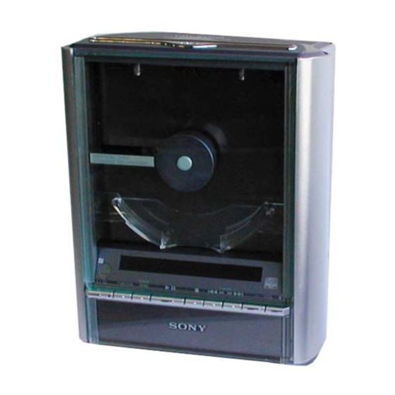
HCD-EX100 is the amplifier, CD
and tuner section in CMT-EX100.
Amplifier section
For the U.S. model
AUDIO POWER SPECIFICATIONS
POWER OUTPUT AND TOTAL HARMONIC
DISTORTION:
With 4 ohms loads, both channels driven, from
120 – 10,000 Hz; rated 12 watts per channel
minimum RMS power, with no more than 10% total
harmonic distortion from 250 milli watts to rated
output.
Canadian model:
Continuous RMS power output (Reference):
European model:
DIN power output (Rated):12 + 12 watts
Continuous RMS power output (Reference):
Music power output (Reference):
Other models:
DIN power output (Rated):12 + 12 watts
Continuous RMS power output (Reference):
9-873-260-01
2001G0200-1
© 2001.7
Downloaded from
www.Manualslib.com
Inputs
PC/TAPE IN:
Outputs
PC/TAPE OUT:
CD DIGITAL OUT:
PHONES (stereo mini jack):
CD player section
System
Laser
15 + 15 watts
(4 ohms at 1 kHz,
10% THD)
Frequency response
(4 ohms at 1 kHz, DIN)
Tuner section
FM stereo, FM/AM superheterodyne tuner
15 + 15 watts
(4 ohms at 1 kHz,
FM tuner section
10% THD)
Tuning range
North American model:
15 + 15 watts
(4 ohms at 1 kHz,
Other models:
10% THD)
Antenna
Antenna terminals
Intermediate frequency
(4 ohms at 1 kHz, DIN,
AM tuner section
240 V)
Tuning range
12 + 12 watts
Pan-American model:
(4 ohms at 1 kHz, DIN,
220 V)
15 + 15 watts
(4 ohms at 1 kHz,
10% THD, 240 V)
European model:
15 + 15 watts
(4 ohms at 1 kHz,
10% THD, 220 V)
Sony Corporation
Home Audio Company
Shinagawa Tec Service Manual Production Group
manuals search engine
HCD-EX100
Model Name Using Similar Mechanism NEW
Mechanism Type
Base Unit Type
Optical Pick-up Type
SPECIFICATIONS
voltage 250 mV,
impedance 47 kilohms
voltage 250 mV,
impedance 1 kilohms
Optical
accepts headphones of
8 ohms or more
Compact disc and digital
audio system
Semiconductor laser
λ
( =780 nm)
Emission duration:
continuous
20 Hz – 20,000 Hz
87.5 – 108.0 MHz
(100 kHz step)
87.5 – 108.0 MHz
(50 kHz step)
FM wire antenna
75 ohms unbalanced
10.7 MHz
530 – 1,710 kHz
(with the interval set at
10 kHz)
531 – 1,710 kHz
(with the interval set at
9 kHz)
531 – 1,602 kHz
(with the interval set at
9 kHz)
MICRO HI-FI COMPONENT SYSTEM
US Model
Canadian Model
AEP Model
UK Model
E Model
Chinese Model
CDM-60B
KSM-770ACA/Z-NP
KSS-770A/Z-N1
Other models:
531 – 1,602 kHz
(with the interval set at
9 kHz)
530 – 1,710 kHz
(with the interval set at
10 kHz)
Antenna
AM loop antenna
External antenna terminals
Intermediate frequency
450 kHz
General
Power requirements
North American model:
120 V AC, 60 Hz
European model:
230 V AC, 50/60 Hz
Other models:
110 – 240 V AC,
50/60 Hz
Power consumption
40 watts
North American model:
1.8 watts (in standby
mode)
European model:
2.7 watts (in standby
mode)
Dimensions
175 x 222 x 201 mm
(w/h/d, incl. projecting
parts and controls)
Mass
Approx. 3.2 kg
Supplied accessories
Remote commander with
battery (1)
AM loop antenna (1)
FM wire antenna (1)
Speaker cords (2)
Design and specifications are subject to change
without notice.
Advertisement
Table of Contents

Related Manuals for Sony HCD-EX100


Summary of Contents for Sony HCD-EX100
- Page 1 US Model Canadian Model Ver 1.0 2001.07 AEP Model UK Model E Model Chinese Model HCD-EX100 is the amplifier, CD and tuner section in CMT-EX100. Model Name Using Similar Mechanism NEW Mechanism Type CDM-60B Base Unit Type KSM-770ACA/Z-NP Optical Pick-up Type...
-
Page 2: Leakage Test
REPLACE THESE COMPONENTS WITH SONY PARTS FONCTIONNEMENT. NE REMPLACER CES COMPOSANTS WHOSE PART NUMBERS APPEAR AS SHOWN IN THIS QUE PAR DES PIÈCES SONY DONT LES NUMÉROS MANUAL OR IN SUPPLEMENTS PUBLISHED BY SONY. SONT DONNÉS DANS CE MANUEL OU DANS LES SUPPLÉMENTS PUBLIÉS PAR SONY. -
Page 3: Table Of Contents
HCD-EX100 TABLE OF CONTENTS NOTES ON HANDLING THE OPTICAL PICK-UP BLOCK OR BASE UNIT 1. SERVICING NOTE ............4 The laser diode in the optical pick-up block may suffer electrostatic 2. GENERAL ................7 break-down because of the potential difference generated by the charged electrostatic load, etc. -
Page 4: Servicing Note
HCD-EX100 SECTION 1 SERVICING NOTE ADJUSTMENT OF CAM PHASE Absorber Absorber Boss SW lever Boss SW lever Rotate the cam in the arrow direction, and adjust the Insert the cam so that the boss touches the SW lever phase until the boss touches the SW lever shown in at the left shown in the figure. - Page 5 HCD-EX100 Shipment Mode • Mode for setting the state of the unit to the state at shipment. When returning the unit to the customer after completing servicing, set to the shipment mode. Procedure : Connect the power plug to the outlet while pressing the 1/u button.
- Page 6 HCD-EX100 Displaying the CD Text • This unit is equipped with a simple CD text display function. The text is displayed only for the first 20 songs. As it will not be displayed from the 21st song, do not suspect a fault.
-
Page 7: General
HCD-EX100 SECTION 2 GENERAL This section is extracted from instruction manual. Downloaded from www.Manualslib.com manuals search engine... - Page 8 HCD-EX100 Setting the time Remote Control Turn on the system. 1 2 3 4 Press CLOCK/TIMER SET on the remote. Proceed to step 4 when you set the clock for the first time. Press . or > repeatedly to select “CLOCK SET”, then press ENTER on...
-
Page 9: Disassembly
HCD-EX100 SECTION 3 DISASSEMBLY Note: Disassemble the unit in the order as shown below. Rear cover, Bottom plate, Case and Eject board Panel board and Stabilizer Amp block CD block Motor assy, Cam and SW board Base unit and Pick up assy Main board,REG board, Power board Note: Follow the disassembly procedure in the numerical order given. -
Page 10: Panel Board And Stabilizer
HCD-EX100 3-2. PANEL BOARD AND STABILIZER Stabilizer claw Stabilizer Turn the stabilizer claw in the direction Stabilizer of the arrow to remove it from the notch on the stabiholder. Panel board 5 Two screws (+BVTT2.6X8) Remove the Earth clip Flat type wire... -
Page 11: Cd Block
HCD-EX100 3-4. CD BLOCK CD block Connector MAIN board: CN351 Flat type wire (CN301) Screw (BVTT3x5) Connector MAIN board: CN302 Screw (BVTT3x5) Two screws (BVTT3x5) 3 Two screws (BVTT3x5) 3-5. MOTOR ASSY (LOADING BOARD), CAM AND SW BOARD Note: The phase adjustment is required in assembly. -
Page 12: Base Unit And Pick Up Assy
HCD-EX100 3-6. BASE UNIT AND PICK UP ASSY Two screws (BVTP2.6x8) Guide (L) Slider (4) Slider (4) Two screws (PTPWH2.6) Coil spring Two screws (BVTP2.6x8) Slider (1) Coil spring Guide (R) !¡ Two screws (PTPWH2.6) !™ BU holder !£ Screws (PTPWH2.6) !¢... -
Page 13: Electrical Adjustment
HCD-EX100 SECTION 4 ELECTRICAL ADJUSTMENT Note: Clear RF signal waveform means that the shape “◊” can be Note: clearly distinguished at the center of the waveform. 1. CD Block is basically constructed to operate without adjustment. Therefore, check each item in order given. -
Page 14: Diagrams
HCD-EX100 SECTION 5 DIAGRAMS 5-1. CIRCUIT BOARDS LOCATION EJECT BOARD MAIN BOARD LED BOARD AMP BOARD PANEL BOARD REG BOARD SW BOARD POWER BOARD LOADING BOARD Downloaded from www.Manualslib.com manuals search engine... - Page 15 HCD-EX100 WAVEFORMS THIS NOTE IS COMMON FOR PRINTED WIRING – MAIN (1/3) SECTION – BOARDS AND SCHEMATIC DIAGRAMS. (In addition to this, the necessary note is printed in each block.) 4.8Vp-p For schematic diagrams. Note: • All capacitors are in µF unless otherwise noted. pF: µµF 16.9MHz...
-
Page 16: Block Diagrams - Tuner/Cd Section
HCD-EX100 5-2. BLOCK DIAGRAMS – TUNER/CD SECTION – TUNER PACK TU-L L_OUT SECTION • RCH is omitted RDS DECODER TU-R MASTER CONTROL • Signal Path IC451 R_OUT R-CH IC701(1/2) : FM FM_DET_OUT BUFFER Q401 RDS_DATA DATA : CD STREO RDS_CLK... -
Page 17: Block Diagrams - Amp Section
HCD-EX100 – AMP SECTION – R-CH POWER AMP IC801 TAPE REC B2 TM801 TAPE-L SPEAKER IN B2 OUTA OUT2 TU-L IMPEDANCE IN D2 R CH USE 4-16Ω CD-L R-CH IN A2 MUTE R-CH Q113 J101 PRE AMP 9 14 16 11... -
Page 18: Printed Wiring Board - Main Section
HCD-EX100 5-3. PRINTED WIRING BOARD – MAIN SECTION – • See page 14 for Circuit Boards Location. • Semiconductor MAIN BOARD (SIDE A) MAIN BOARD (SIDE B) Location (CHASSIS) Ref. No. Location D139 D701 D751 D752 D753 D754 IC111 IC301... -
Page 19: Schematic Diagram - Main (1/3) Section
HCD-EX100 5-4. SCHEMATIC DIAGRAM – MAIN (1/3) SECTION – • See page 15 for Waveforms. • See page 33,34,35 for IC Block Diagrams. • See page 30 for IC Pin Functions. Downloaded from www.Manualslib.com manuals search engine... -
Page 20: Schematic Diagram - Main (2/3) Section
HCD-EX100 5-5. SCHEMATIC DIAGRAM – MAIN (2/3) SECTION – Downloaded from www.Manualslib.com manuals search engine... -
Page 21: Schematic Diagram - Main (3/3) Section
HCD-EX100 5-6. SCHEMATIC DIAGRAM – MAIN (3/3) SECTION – • See page 14 for Waveforms. • See page 35 for IC Block Diagrams. • See page 31 for IC Pin Functions. Downloaded from www.Manualslib.com manuals search engine... -
Page 22: Printed Wiring Board - Led/Loading/Sw/Amp Section
HCD-EX100 5-7. PRINTED WIRING BOARD – LED/LOADING/SW/AMP SECTION – • See page 14 for Circuit Boards Location. (Page 18) MAIN MAIN • Semiconductor BOARD BOARD Location TP772 TP771 LED BOARD (SIDE A) Ref. No. Location AMP BOARD (SIDE A) AMP BOARD (SIDE B) -
Page 23: Schematic Diagram
HCD-EX100 5-8. SCHEMATIC DIAGRAM – LED/LOADING/SW/AMP SECTION – • See page 35 for IC Block Diagrams. Downloaded from www.Manualslib.com manuals search engine... -
Page 24: Printed Wiring Board - Panel/Eject Section
HCD-EX100 5-9. PRINTED WIRING BOARD – PANEL/EJECT SECTION – • See page 14 for Circuit Boards Location. • Semiconductor Location PANEL BOARD (SIDE A) Ref. No. Location D621 D650 D651 IC601 IC651 MAIN IC652 BOARD CN701 Q622 EJECT BOARD (SIDE A) -
Page 25: Schematic Diagram - Panel/Eject Section
HCD-EX100 5-10. SCHEMATIC DIAGRAM – PANEL/EJECT SECTION – Downloaded from www.Manualslib.com manuals search engine... -
Page 26: Printed Wiring Board - Reg Section
HCD-EX100 5-11. PRINTED WIRING BOARD – REG SECTION – • See page 14 for Circuit Boards Location. • Semiconductor Location REG BOARD (SIDE A) REG BOARD (SIDE B) Ref. No. Location D933 D934 D961 IC931 IC932 Q961 (CHASSIS) Q962 Q963... -
Page 27: Schematic Diagram - Reg Section
HCD-EX100 5-12. SCHEMATIC DIAGRAM – REG SECTION – Downloaded from www.Manualslib.com manuals search engine... -
Page 28: Printed Wiring Board - Power Section
HCD-EX100 5-13. PRINTED WIRING BOARD – POWER SECTION – • See page 14 for Circuit Boards Location. • Semiconductor Location Ref. No. Location (CHASSIS) POWER BOARD D901 D911 D931 D941 D951 D952 D953 D954 IC933 IC951 BOARD CN904 (Page 26) -
Page 29: Printed Wiring Board - Power Section
HCD-EX100 5-14. SCHEMATIC DIAGRAM – POWER SECTION – Downloaded from www.Manualslib.com manuals search engine... - Page 30 HCD-EX100 5-15. IC PIN FUNCTIONS • IC303 DIGITAL SERVO & DIGITAL SIGNAL PROCESSOR (CXD2585Q) (MAIN Board (1/3)) Pin No. Pin Name Function Pin No. Pin Name Function Tracking error signal input DVDD Power supply Center servo analog input (Connected to ground) XRST System reset input “L”...
- Page 31 HCD-EX100 • IC701 uCOM (UPD780306GF-034-3BA) (MAIN Board (3/3)) Pin No. Pin Name Function TUNED ST tuning PLL_CE ST PLL CE signal output PLL_DATAI ST PLL data input PLL_DATAO ST PLL data output PLL_CLK ST PLL CLK VPP (GND) – Ground...
- Page 32 HCD-EX100 Pin No. Pin Name Function 51 to 54 COM0 to COM3 LCD common output BIAS LCD bias voltage terminal 56 to 58 VLC0 to VLC2 LCD bias voltage terminal VSS0 Ground 60 to 99 SEG0 to SEG39 LCD segment signal output...
-
Page 33: Ic Block Diagrams
HCD-EX100 5-16. IC BLOCK DIAGRAMS IC301 CXA2568M-T6 (MAIN board (1/3)) APC PD AMP LC/PD LD_ON HOLD AGCVTH VREF APC LD AMP HOLD_SW AGCCONT RF_BOT RFTC RF SUMMING AMP RF_EQ_AMP ERROR AMP FOCUS TRACKING ERROR AMP VC BUFFER IC304 PCM1710U-B/1K (MAIN board (1/3)) - Page 34 HCD-EX100 IC303 CXD2585Q (MAIN board (1/3)) 71 70 67 66 65 64 63 62 61 Digital VPCO DVDD0 Clock V16M Generator XRST VCTL MUTE Interface BIAS Error AVDD1 Corrector DATA XLAT CLOCK FILI Digital Interface Sub Code FILO demodurator Processor...
- Page 35 HCD-EX100 IC302 BA5974FP-E2 (MAIN board (1/3)) MUTE INTERFACE LEVEL SHIFT THERMAL SHUTDOWN INTERFACE INTERFACE IC451 BU1924F (MAIN board (3/3)) CLOCK TEST DEFFERENTIAL BIPHASE PLL 57KHz DECODER DECODER 1187.5Hz RDS/ARI 8TH SWITCHED CAPACITOR FILTER IC351 BA6956AN (LOADING board) CONTROL LOGIC Downloaded from www.Manualslib.com...
-
Page 36: Exploded Views
HCD-EX100 SECTION 6 EXPLODED VIEWS NOTE: The components identified by • The mechanical parts with no reference number in • -XX, -X mean standardized parts, so they may have mark ! or dotted line with mark the exploded views are not supplied. -
Page 37: Chassis Section
HCD-EX100 6-2. CHASSIS SECTION not supplied not supplied LCD701 not supplied 51 59 not supplied not supplied not supplied not supplied not supplied not supplied not supplied Les composants identifiés par une The components identified by marque ! sont critiques pour la mark ! or dotted line with mark ! are critical for safety. -
Page 38: Mechanism Section
HCD-EX100 6-3. MECHANISM SECTION M351 Ref. No. Part No. Description Remark Ref. No. Part No. Description Remark 4-236-397-01 DECORATION (CD) 4-225-227-01 SPRING (ABSORBER),TENSION COIL 4-222-701-01 PANEL, MECHANICAL 4-225-228-01 CAM (A) 4-985-672-01 SCREW (+PTPWHM2.6), FLOATING 4-225-226-01 ABSORBER 4-222-697-01 RUBBER, FLOATING 4-222-689-01 SLIDER (3) -
Page 39: Base Unit Section
HCD-EX100 SECTION 7 EJECT ELECTRICAL PARTS LIST Note: • SEMICONDUCTORS • Due to standardization, replacements in the parts list The components identified by In each case, u: µ , for example: may be different from the parts specified in the mark ! or dotted line with mark uA...: µ... -
Page 40: Electrical Parts List
HCD-EX100 LOADING EJECT MAIN Ref. No. Part No. Description Remark Ref. No. Part No. Description Remark < IC > < CAPACITOR > IC651 8-759-673-48 IC SN74HC14ANSR C100 1-163-263-11 CERAMIC CHIP 330PF IC652 8-759-925-90 IC SN74HC74ANSR C101 1-163-251-11 CERAMIC CHIP 100PF... - Page 41 HCD-EX100 MAIN Ref. No. Part No. Description Remark Ref. No. Part No. Description Remark C323 1-163-235-11 CERAMIC CHIP 22PF C452 1-163-031-91 CERAMIC CHIP 0.01uF C324 1-163-038-91 CERAMIC CHIP 0.1uF (AEP,UK) C325 1-163-009-91 CERAMIC CHIP 0.001uF C453 1-163-006-11 CERAMIC CHIP 560PF...
- Page 42 HCD-EX100 MAIN Ref. No. Part No. Description Remark Ref. No. Part No. Description Remark R116 1-216-094-00 RES-CHIP 1/10W < FERRITE BEAD > R117 1-216-085-91 RES-CHIP 1/10W FB300 1-500-245-11 FERRITE R131 1-216-025-11 RES-CHIP 1/10W FB331 1-500-245-11 FERRITE R132 1-216-025-11 RES-CHIP 1/10W...
- Page 43 HCD-EX100 MAIN PANEL Ref. No. Part No. Description Remark Ref. No. Part No. Description Remark R364 1-216-025-11 RES-CHIP 1/10W R754 1-216-089-91 RES-CHIP 1/10W R365 1-216-025-11 RES-CHIP 1/10W R755 1-216-089-91 RES-CHIP 1/10W R381 1-216-061-91 RES-CHIP 3.3K 1/10W R756 1-216-073-91 RES-CHIP 1/10W...
- Page 44 HCD-EX100 POWER PANEL Ref. No. Part No. Description Remark Ref. No. Part No. Description Remark C905 1-163-038-91 CERAMIC CHIP 0.1uF R616 1-216-065-91 RES-CHIP 4.7K 1/10W C911 1-107-425-11 CERAMIC 470PF R619 1-216-061-91 RES-CHIP 3.3K 1/10W C912 1-131-969-11 ELECT 1800uF R622 1-216-041-00 METAL CHIP...
- Page 45 HCD-EX100 POWER Ref. No. Part No. Description Remark Ref. No. Part No. Description Remark < CAPACITOR > < IC > C891 1-164-159-11 CERAMIC 0.1uF 8-749-019-48 IC STR-F6676-LF1352 C892 1-164-159-11 CERAMIC 0.1uF IC933 8-759-288-53 IC LA5617 C893 1-164-159-11 CERAMIC 0.1uF IC951...
- Page 46 HCD-EX100 Ref. No. Part No. Description Remark Ref. No. Part No. Description Remark R961 1-216-073-91 RES-CHIP 1/10W **************** HARDWARE LIST R962 1-216-049-11 RES-CHIP 1/10W **************** R963 1-249-417-11 CARBON 1/4W 7-685-870-01 SCREW +BVTT 3X5 (S) < TERMINAL > 7-685-246-14 SCREW +KTP 3X8 TYPE2 NON-SLIT...
- Page 47 HCD-EX100 MEMO Downloaded from www.Manualslib.com manuals search engine...
- Page 48 HCD-EX100 REVISION HISTORY Clicking the version allows you to jump to the revised page. Also, clicking the version at the upper right on the revised page allows you to jump to the next revised page. Ver. Date Description of Revision 2001.
Need help?
Do you have a question about the HCD-EX100 and is the answer not in the manual?
Questions and answers