Table of Contents
Advertisement
Quick Links
See also:
User Manual
SERVICE MANUAL
DOCUMENTATION TECHNIQUE
TECHNISCHE DOKUMENTATION
DOCUMENTAZIONE TECNICA
DOCUMENTACION TECNICA
WARNING : Before servicing this chassis please read the safety recommendations.
ATTENTION : Avant toute intervention sur ce châssis, lire les recommandations de sécurité.
ACHTUNG : Vor jedem Eingriff auf diesem Chassis, die Sicherheitsvorschriften lesen.
ATTENZIONE : Prima di intervenire sullo chassis, leggere le norme di sicurezza.
IMPORTANTE : Antes de cualquier intervención, leer las recomendaciones de seguridad.
- 1004
No copying, translation, modification on other use authorized. All rights reserved worldwide. • Tous droits de reproduction, de traduction, d'adaptation et d'exécution réservés pour tous les pays. • Sämtliche Urheberrechte an diesen Texten und Zeichnunge n stehen uns zu. Nachdrucke,
Vervielfältigungen - auch auszugsweise - nur mit unserer vorherigen Zustimmung zulässig. Alle Rechte vorbehalten. • I diritti di riproduzione, di traduzione, e esecuzione sono riservati per tutti i paesi. • Derechos de reproduccion, de traduccion, de adaptacion y de ejecucion reservados para todos los paises.
T V
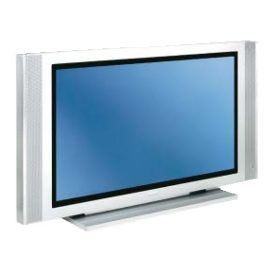
42WM03ST
42WM04ST
Plasma
Advertisement
Table of Contents

Related Manuals for THOMSON 42WM03ST


Summary of Contents for THOMSON 42WM03ST
- Page 1 SERVICE MANUAL DOCUMENTATION TECHNIQUE 42WM03ST TECHNISCHE DOKUMENTATION 42WM04ST DOCUMENTAZIONE TECNICA DOCUMENTACION TECNICA Plasma WARNING : Before servicing this chassis please read the safety recommendations. ATTENTION : Avant toute intervention sur ce châssis, lire les recommandations de sécurité. ACHTUNG : Vor jedem Eingriff auf diesem Chassis, die Sicherheitsvorschriften lesen.
- Page 2 Do not disconnect modules when they are energized! Repairs on power supply section are to be carried out only with isolating transformer. Ne pas retirer les modules lorsqu' ils sont sous tension. N'effectuer les travaux de maintenance sur la partie reliée au secteur (Switch Mode) qu'au travers d'un transformateur d'isolement.
-
Page 3: Table Of Contents
CONTENTS Page SAFETY PRECAUTIONS ............4 DISASSEMBLY Removing the leg tube assembly . -
Page 4: Safety Precautions
IMPORTANT SAFETY PRECAUTIONS 1. Before returning an instrument to the customer, always make a safety check of the entire instrument, including the following items, but not limited to them. a. Be sure that no built-in protective devices are defective and/or have been defeated during servicing. (1) Protective shields are provided on this chassis to protect both the technician and the customer. - Page 5 3. Design Alteration Warning: Do not alter or add to the mechanical or electrical design of this unit. Design alterations and additions, including, but not limited to, circuit modifications and the addition of the items such as auxiliary audio and/or video output connections might alter the safety characteristics of this Projection Monitor and create a hazard to the user.
-
Page 6: Removing The Leg Tube Assembly
HOW TO EXCHANGE THE MASK & PANEL PROCEDURE 1. Removing the Leg Tube Assembly Unscrew 4 screws from "Leg Tube Assembly." (Specification of screw driver is 15± 2kg), see fig.1 Fig. 1 Push the "Leg Tube Assembly." downward to unlock and pull it away from unit, then unscrew 4 screws from rear cover. (Specification of screw -driver is 15±... -
Page 7: Removing The Rear Cover
2. Removing the rear cover Unscrew 12 screws from rear cover, see red arrow (Specification of screw driver is 15± 2 kg) Unscrew 8 screws from rear cover, and unscrew 2 screws from AC power socket, see red arrow (Specification of screw driver is 9±... -
Page 8: Removing The Filter
4. Removing the Mask and the J5 cable from PCB Fig. 5 5. Removing the filter Unscrew 10 screws from mask (Specification of screw driver is 15± 2 kg), then remove four angles that hold the PDP filter. (Be careful: Please do not bump or scrape when handling the PDP filter.) Before putting panel back clean PDP filter make sure it's free from dust. - Page 9 Remove the Control buttons from old Mask and reinstall them on the new Mask. Control buttons Fig. 8 Please to aim at red arrow to guide and there is have a channel when you put down glass back to new mask Fig.
-
Page 10: Troubleshooting
TROUBLESHOOTING No power Switch the power on Replace Not correct Check "Power Switch" module "Power Switch" module Correct Replace "Main Power" module First issue 10 /04... -
Page 11: No Picture
No picture Replace Not correct Check Image board Image board Correct Replace PDP module First issue 10 / 04... -
Page 12: Vertical Line Fail
Vertical line fail Replace Not correct Check XR Board Board Correct Replace Not correct Check Logic Board Logic Board Correct Replace PDP module First issue 10 /04... -
Page 13: Horizontal Line Fail
Horizontal line fail Replace Not correct Check Y-SUS Board Y-SUS Board Correct Replace Not correct Check Y DRV-Top Y DRV-Top Correct Not correct Replace Y Check Y DRV-Bottom DRV-Bottom Correct Replace Not correct Check Z-SUS Board Z-SUS Board Correct Replace PDP module First issue 10 / 04... -
Page 14: No Command
No command Switch the power on Replace the Not correct Check remote control battery or the remote control Correct Replace Not correct Check Front Button Front Button Control Board Control Board Correct Replace Image Board First issue 10 /04... -
Page 15: Adjustments
ADJUSTMENTS PANEL voltage adjustment 1.1 Origin Power (PLG-421) CN806 RV203 RV204 1. POWER ON 2. Signal Source: No (black screen). 3. Connect Digital Voltage Meter (-) to Panel GND. Connect Digital Voltage Meter (+) to Plug CN806 Pin#10 and adjust the VA (Variable Resistor RV204) value to the VA value recorded on the Panel Voltage Label ±... - Page 16 1.2 Dae Gil Power (DGK-420W) 1. POWER ON 2. Signal Source: No (black screen). 3. Connect Digital Voltage Meter (-) to Panel GND. Connect Digital Voltage Meter (+) to Plug CN806 Pin#10 and adjust the VA (Variable Resistor) value to the VA value recorded on the Panel Voltage Label ± 0.5VDC (VA ± 0.5VDC= value adjusted). 4.
- Page 17 2. Turn on Color Analyzer CA-100 and reset CA-100. 3. Switch PDP input signal source to DVI mode. 4. Set up Video Pattern Generator (Astro, Model= VG-828H). Timing set = 640 x 480 @ 60Hz; Video = Panel Link (the DVI output mode) Connect PDP DVI input connector with Astro to receive DVI signal.
- Page 18 1.2 Adjusting procedure 1. Receive Astro VG-828H DVI dark level center block signal (14 IRE), follow the ”Factory Setting Procedure” to go into factory setting mode and you will see the 7180K color temperature setting OSD menu. 2. 7180K dark level center block adjustment procedure: A.
- Page 19 Factory Setting Procedure: A. Press (Zoom -) key for over 5 seconds and release. B. Press (Zoom+) key for over 5 seconds and release. C. Press ”ok” key. D. Factory setting OSD menu shows up. The values showed up on the OSD menu are the factory default setting values. The factory default setting values differ from each PDP panel module.
- Page 20 2. Switch PDP input signal source to AV mode. 3. Set up Video Pattern Generator (Astro, Model= VG-828H). Timing set = 640 x 480 @ 60Hz; Video = Analog (the AV output mode) Connect PDP AV input connector with Astro to receive AV signal. 4.
- Page 21 and BIAS Gamma values are correct, and then press the ”ok” key in remote control. For each color temperature setting, please repeat the procedure (1)-(3). Only x and y value will change in different color temperature mode (in 8680K, x=288, y=301;...
-
Page 22: Power (Plg-421)
3. 7180K bright level center block adjustment procedure: (Please set Astro VG-828H RGB bright level center block signal to 60 IRE) A. Press (Zoom -) or (Zoom+) key in remote control to select G-GAIN, and adjust Y=41±2FL B. Press (Zoom -) or (Zoom+) key in remote control to select R-GAIN, and adjust x=308±15FL C. - Page 23 Mode list for RGB / DVI Refresh Horizontal Vertical Vertical Horizontal Mode No Resolution Rate Frequency Frequency Sync Sync Dot rate Polarity Polarity (Hz) (K Hz) (Hz) (TTL) (TTL) (MHz) 640(VGA)x480 31.5 59.94 25.175 640(VGA)x480 37.9 72.81 31.500 640(VGA)x480 37.5 31.500 640(VGA)x480 43.3...
-
Page 24: Appendix A
APPENDIX A : Preset Timing Chart Item Description: Total time Active display area including borders Active display area excluding borders Left/Top border Right/bottom border Blanking time Front porch Sync -width Back porch Mode No Resolution & Refresh Rate Pixel clock 25.175 31.5 31.5... - Page 25 Mode No Resolution 1024 1024 1024 1024 1280 1280 1280 & 1024 1024 1024 Refresh Rate Pixel clock 78.75 94.5 157.5 28.320 25.175 Horizontal visible 1024 1024 1024 1024 1280 1280 1280 Dots Horizontal total 1344 1328 1312 1376 1688 1688 1728 Dots...
-
Page 26: Wiring Diagram
WIRING DIAGRAM PDP Module Audio Amplifier CN803 CN802/CN809 Board Ass'y Image Board Ass'y AV Module (TMDS) (5V,SB DET) Board(with Main Power Tuner) Assy (24V,9V) Y-SUS Z-SUS CN801 (RLYON VSON) (Audio Signal) (9V) (Audio DC,Supply) (5V) (Key) Front Button AC_IN Control CN02 CN03 Board... -
Page 27: Block Diagram
BLOCK DIAGRAM Tuner Board Signal Block Diagram MAIN Board Signal Block Diagram for SUB-picture SDRAM RGB I/P RGB O/P U48,49 Connector Connector TUNER JPT1 (48 Pin) (48 Pin) 6630/6730 MAIN Video S-VIDEO S-VIDEO Processor TV_CVBS TV_CVBS TA8551CH COMPOSITE(AV) COMPOSITE(AV) YCBCR SWITCH SDRAM COMPOSITE(AV) - Page 28 TUNER BOARD SCHEMATIC DIAGRAM: TUNER & MSP RT162 1/16W RT160 P[3,5] 1/16W RT202 SCART_OUT_CVBS P[2] RT37 1/16W + CT157 CT180 FQ1216MEIH3 10uF 0.1uF 1/16W 1/16W QT15 2SC2412KBQ ANT IN ICT1 LA7213 2SA1037KQ RT161 4.7K 0.47uF 16V 4.7K 1/16W 1/16W 1/16W RT11 1/16W RT12...
- Page 29 TUNER BOARD SCHEMATIC DIAGRAM: SOURCE INPUT RT61 SOUND_OUT_R P[1] 1/16W 120 Ω CT82 RT58 CT169 RT97 120 Ω 1000PF 470PF P[1] SOUND_IN_R 1/16W SOT1 1/16W JT1A FBT6 CT81 RT60 CT166 CS1630-1---- 120 Ω M1076-1--- A 470PF 220PF SCART_L 1/16W AUX_OUT_L P[1] CT170 RT104 R O/P...
- Page 30 TUNER BOARD SCHEMATIC DIAGRAM: UOC 470 1/16W RT110 RT134 470 1/16W RT111 LT13 LT14 15uH 1/16W 15uH 470 1/16W RT112 BOUT P[4] CT182 RT138 CT183 10uH N/1K 1/16W T CT181 RT113 TPT4 68PF 33PF 33PF 1/16W N/100 1/16W RT115 TPT5 P[5] TPT6 CT179...
- Page 31 TUNER BOARD SCHEMATIC DIAGRAM: SYNCHRONISATION & RGB TO YUV P9V P[1,5] CT142 CT143 47uF 0.1uF RT127 1/16W RT132 3.3K CT185 CT184 1/16W 22PF 22PF ICT7 CT144 TA1287P 0.1uF RT129 V IN Matrix T CT186 CT145 2.2K P[3] BOUT 22PF 0.1uF 1/16W RT130 Y IN...
- Page 32 TUNER BOARD SCHEMATIC DIAGRAM: CONNECTIONS JPT2A CP1615-148-B JPT2B P[1,4] CP1615-148-B CTL1 RT164 0 1/16W (LINK O/P) P[3] CTL1 RT102 N/0 1/16W TP21 RT165 0 1/16W CTL2 (LINK I/P) P[3] CTL2 RT178 N/0 1/16W TP25 SCL2 FBT1 P[1,3] SCL2 RT106 N/0 1/16W TP22 120 Ω...
-
Page 33: Main
P[0..7] MAIN BOARD SCHEMATIC DIAGRAM: DIGITAL SYSTEM (CPU & EEPROM) P[0..7] P[13] A[0..19] SB5V_CPU 10K 1/16W SB5V_CPU 10K 1/16W N/W27C010_5 10K 1/16W EEPROM(DIP32) N/1.5K N/1.5K SB5V 74LVT04 74LVT04 1/16W 1/16W TDO P[18] TDI P[18] 1/8W TMS P[18] SB5V_CPU TCK P[18] LD001 LD002 N/LED... - Page 34 MAIN BOARD SCHEMATIC DIAGRAM: DIGITAL SYSTEM (OSD/USB/RS232) 5V_OSD 1/16W 1/8W MTV130 N/1K N/1K N/1K P[3] POCLKOSD 1/16W 1/16W 1/16W 1/16W R_OSD P[5] R-OUT D(3) 1/16W T C416 22PF 10uF 0.1uF RP12 G_OSD P[5] G-OUT 1/16W 10K ohm G(1) S(2) SDA2_33 P[4,7,13,18] SDA2_33 BSN20...
- Page 35 MAIN BOARD SCHEMATIC DIAGRAM: DIGITAL SYSTEM (HSYN SW & CLOCK GEN.) 74LVC157 1/16W PIHS P[5] P[8] DVI_HS DDCVSYNC P[7] P[7] PLLHSO PIVS P[5] P[8] DVI_VS 1/16W FGVS P[7,8,9] FGVS PICLK P[5] R386 P[5] DVI_PICK 1/16W 150 1/16W C404 22PF V33SB P[7] DATACK PIHSS...
- Page 36 MAIN BOARD SCHEMATIC DIAGRAM: DIGITAL SYSTEM (BUFFER & PDP CONNECTOR) 74LVC244ADB R382 1/16W PCLK_LG BPCLKO TP20 POCLK N/22 1/16W P[3,5] POCLK TP14 TP17 74LVC244ADB ROUT[0..7] RP36 BVSYNCO VSYNCO DSVSYNCO P[5] ROUT[0..7] 22 ohm P[2,5] VSYNCO TP15 TP18 DSHSYNCO BRROUT0 ROUT7 BROUT7 BROUT0 HSYNCO...
- Page 37 MAIN BOARD SCHEMATIC DIAGRAM: DIGITAL SYSTEM (IMAGE SCALING) MA_IP11 TP22 74LVC157 MA_IP13 TP23 PCSI P[18] PCSI MA_IP[0..13] P[6] N/CON6 P[1] VIP711 PCn_MPU SSCS PCSCS MD_IP[0..47] P[6] PCSI PCSCS P[18] PCSCS PCSCLK CSn_IP P[6] RASn_IP P[6] P[1] CASn_IP P[6] 1/16W SO P[1] WRn_IP P[6] LDQM...
- Page 38 MAIN BOARD SCHEMATIC DIAGRAM: DIGITAL SYSTEM (IMAGE SDRAM 16M) P[5] MA_IP[0..13] P[5] MD_IP[0..47] M12L16161A M12L16161A M12L16161A MD_IP32 MA_IP0 MD_IP33 MA_IP1 MD_IP16 MA_IP0 MD_IP34 MA_IP2 MD_IP17 MA_IP1 MD_IP0 MA_IP0 MD_IP35 MA_IP3 MD_IP18 MA_IP2 MD_IP1 MA_IP1 MD_IP36 MA_IP4 MD_IP19 MA_IP3 MD_IP2 MA_IP2 MD_IP37 MA_IP5 MD_IP20...
- Page 39 MAIN BOARD SCHEMATIC DIAGRAM: DIGITAL SYSTEM (FLAT PANEL INTERFACE) V33PLL VDD33 V33PLL V33PLL BA033LBSG 200 Ω C105 C106 C107 C100 C101 C102 C103 C104 V33ADC 0.1uF 0.01uF 10uF 0.1uF 0.1uF 0.1uF 0.1uF 0.1uF 0.1uF 1/16W PID[0..7] P[5,8] PID0 DRA0 RP10 DRA0 PID1 VDD33...
- Page 40 MAIN BOARD SCHEMATIC DIAGRAM: DIGITAL SYSTEM (PANEL LINK RECEIVER DVI SIL161) 120 Ω/2A V33SB T128A-BJST T128A-BJST TMDSD2P RX2P SII161BCT RX2N TMDSD2N TMDSD1P RX1P TMDSD1N RX1N 1/8W PID[40..47] P[5,7] 120 Ω/2A TMDSD0P RX0P TMDSD0N RX0N VDVIA VDVID RP23 PID40 OVCC TMDSCP RXCP 33 ohm PID41...
- Page 41 MAIN BOARD SCHEMATIC DIAGRAM: DIGITAL SYSTEM (VGA INPUT/OUTPUT) R353 SB5V_V R383 1/16W 1/16W P[19] R354 0 1/16W R157 P[19] C161 + C160 0.1uF 1/16W RLS4148 22uF R377 SB5V_V P[19] R351 1/16W U35 Socket C168 BA7657F I1177-108-- R369 VGA_5V 0.01uF 1/16W R158 1/16W N/4.7...
- Page 42 MAIN BOARD SCHEMATIC DIAGRAM: VIDEO SYSTEM (AUDIO & VIDEO SWITCH) C183 DVI_R R171 N/3.3K N/2.2uF RGB_R P[18] DV1_R RGB_R P[18] 1/16W DVI_R R173 DVI_R P[18] DVI_L N/3.3K C184 RGB_L P[18] DVI_L RGB_L P[18] 1/16W N/2.2uF DVI_L DVI_L P[18] C213 N/0.1uF R175 R172 R174...
- Page 43 MAIN BOARD SCHEMATIC DIAGRAM: VIDEO SYSTEM (YUV SWITCH) C214 10uF P[18] PB2_CB2 R358 R229 C222 1/16W C217 1/16W 10uF M52055FP R230 PTV_Y PTV_Y0 47uF 1/16W I/P 1A GND 1 M52055FP R232 P[18] 3.9K GND 2 R359 1/16W I/P 1A GND 1 GND 3 1/16W GND 2...
- Page 44 MAIN BOARD SCHEMATIC DIAGRAM: VIDEO SYSTEM (COLOR SPACE) C266 C267 R257 C268 R258 100uF 22uF 0.1uF 1/16W 1/16W R260 R261 P[11] PR_IN R381 R380 1/16W 1/16W P[11] PB_IN 1/16W 1/16W 2SC2412KBQ P[11] Y0_IN R259 R262 YPBPR_R P[9] 1/16W 1/16W R355 C270 C271 C269...
- Page 45 MAIN BOARD SCHEMATIC DIAGRAM: VIDEO SYSTEM (PANEL TV MAIN PICTURE) P[15] DQM_MP[0..7] P[15] MA_MP[0..9] BA_MP BA_MP P[15] P[15] MD_MP[0..63] RASn_MP RASn_MP P[15] V25_MP CASn_MP CASn_MP P[15] WEn_MP WEn_MP P[15] CS0n_MP CS0n_MP P[15] MCLK_MP MCLK_MP P[15] 1/16W 1/16W 1/16W 1/16W AVDD1 P[15] AVDD1 1/16W...
- Page 46 MAIN BOARD SCHEMATIC DIAGRAM: VIDEO SYSTEM (PANEL TV SUB PICTURE) P[16] DQM_SP[0..7] BA_SP BA_SP P[16] P[16] MA_SP[0..9] RASn_SP RASn_SP P[16] P[16] MD_SP[0..63] CASn_SP CASn_SP P[16] V25_SP WEn_SP WEn_SP P[16] RDS3 CS0n_SP CS0n_SP P[16] MCLK_SP MCLK_SP P[16] 1/16W HSPIP P[13] RDS2 RDS1 RDS4 1/16W...
- Page 47 MAIN BOARD SCHEMATIC DIAGRAM: VIDEO SYSTEM (PANEL TV MP SGRAM) Place these resistors close to DPTV VADC3 RD29 33 1/16W BAMP P[13] BA_MP RD30 33 1/16W WEnMP P[13] WEn_MP AVDDA1 P[13] RD31 33 1/16W CASnMP P[13] CASn_MP RD32 33 1/16W CD37 RASnMP + CD36...
- Page 48 MAIN BOARD SCHEMATIC DIAGRAM: VIDEO SYSTEM (PANEL TV SP SGRAM) VADC3_S Place these resistors close to DPTV RDS29 1/16W BASP P[14] BA_SP RDS30 1/16W WEnPS AVDDA1_S P[14] P[14] WEn_SP RDS31 1/16W CASnSP P[14] CASn_SP RDS32 1/16W LDS3 CDS36 CDS37 RASnSP P[14] RASn_SP 10uF...
- Page 49 MAIN BOARD SCHEMATIC DIAGRAM: VIDEO SYSTEM (POWER REGULATOR) REG_5V REG_5V_S VCCA3 5VDDA 5VDDA_S VCCA3_S BA033 BA033 5VDDA_ VCCA3 5VDDA_S_ VCCA3_S VOUT VOUT CD86 LDS13 CDS85 CDS82 CDS86 LD14 CD85 + CDS84 + CD82 CD84 0.1uF 0.1uF 22uF 0.1uF 0.1uF 22uF 1/8W 22uF 22uF...
- Page 50 MAIN BOARD SCHEMATIC DIAGRAM: VIDEO SYSTEM (CONNECTOR) +24V P24V N/P1079-1-2-- N/2.2uF TO AUDIO PWB +5V A DVI/RGB CP0053-JJST- SB5V CP031C-EJST- + C333 C380 C334 N/1000PF N/47K 330uH 220uF 0.22uF 0.22uF C240 C421 1/16W 1/16W 47uF 0.1uF CP031A-EJST- L_IN P[10] P[10] R_IN L_OUT N/P1079-1-2--...
-
Page 51: Main
MAIN BOARD SCHEMATIC DIAGRAM:VIDEO SYSTEM (VGA INPUT/OUTPUT) C159 0.01uF RA171 0 1/16W VGA_RIN RINA P[9] VGA_RIN RA172 0 1/16W RA353 R149 T C176 C162 100PF 47uF 1/16W 1/8W 1/16W RA354 SB5V_V SB5V_V C163 1/16W BAV99 0.01uF RA383 N/10 RGB_GIN 1/16W P[9] RGB_GIN RA351... -
Page 52: Special Mode
Special Modes Action Remarks Operation Switch the Set Off. Press & Hold "Menu" key of local keyboard. Switch the Set On. "OUT OF BOX" condition The set must switch to On mode and then to Standby mode. Switch the set to On mode. Select Language and Auto Installation is then displayed. - Page 53 UOC Service Menu Press "Down" or Up" key of the remote control in order to turn the page. UOC SW version 031128 031221 MCU SW version 031117 Page Parameter Default Value Default Value Init TV* Sharp-PTV AGC INT Contrast Color Brightness WPR-C WPG-C...
-
Page 54: Exploded View
EXPLODED VIEW Description FRONT PANEL POWER/INPUT BUTTON MENU/VOLUME BUTTON KEYBOARD FRONT GLASS FILTER PDP Module AUDIO STAND-BY POWER BOARD 17 20 17 17 AUDIO AMPLIFIER BOARD 17 25 RIGHT TOP SPEAKER HOLDER SPEAKER LEFT TOP SPEAKER HOLDER RIGHT BOTTOM SPEAKER HOLDER POWER SWITCH BOARD ON/OFF BUTTON LEFT BOTTOM SPEAKER HOLDER... - Page 55 46, quai Alphonse Le Gallo Czech s.r.o. 92648 Boulogne cedex ul. Dopravaku - dum Genius 1 Tel. : 01 41 86 60 00 Dolni Chabry Internet : www.thomson-network.com CZ - 18400 Prague 8 Tel. : (2) 688 67 70 Thomson multimedia Thomson multimedia Switzerland...
Need help?
Do you have a question about the 42WM03ST and is the answer not in the manual?
Questions and answers