Table of Contents
Advertisement
Ver. 2
Please refer to the
MODIFICATION NOTICE.
SERVICE MANUAL
MODEL
JP
E3
E2
EK
E2A E1C E1K EUT
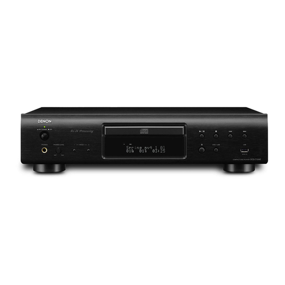
DCD-710AE
CD PLAYER
●
For purposes of improvement, specifications and design are subject to change without notice.
●
Please use this service manual with referring to the operating instructions without fail.
●
Some illustrations using in this service manual are slightly different from the actual set.
e
D&M Holdings lnc.
S0009-0V02DM/DG0911
Copyright 2009 D&M Holdings Inc. All rights reserved.
WARNING: Violators will be prosecuted to he maximum extent possible.
Advertisement
Table of Contents

Related Manuals for Denon DCD-710AE


Summary of Contents for Denon DCD-710AE
- Page 1 Please refer to the MODIFICATION NOTICE. SERVICE MANUAL MODEL E2A E1C E1K EUT DCD-710AE CD PLAYER ● For purposes of improvement, specifications and design are subject to change without notice. ● Please use this service manual with referring to the operating instructions without fail.
-
Page 2: Laser Radiation
DCD-710AE... - Page 3 DIMENSION DCD-710AE...
-
Page 4: Wire Arrangement
If wire bundles are untied or moved to perform adjustment or parts replacement etc.,be sure to rearrange them neatly as they were originally bundled or placed afterward. Otherwise, incorrect arrangement can be a cause of noise generation. Wire arrangement viewed from the top Front Panel side Back Panel side DCD-710AE... - Page 5 • Refer to the table below for a description of the direction in which the photos were taken. • Photographs for which no direction is indicated were taken from above the product. The viewpoint of each photograph (photography direction) Front side [View from above] Direction of photograph: A DCD-710AE...
-
Page 6: Top Cover
1. DOOR → Proceeding : TOP COVER DOOR (1) Take off the Chucking plate after removing screws. Chucking plate (2) Open the CD tray by turning the Drive gear clockwise. Drive gear CD tray (3) Detach the DOOR. DOOR DCD-710AE... -
Page 7: Front Panel Assy
View from bottom (2) Cut the clamp bands, disconnect the connector wires and FFC Cable Remove the screws.. FFC Cable BN33 BN31 CN51 CX73 Please refer to "EXPLODED VIEW" for the disassembly method of each PCB included in FRONT PANEL ASSY. DCD-710AE... -
Page 8: Cd Mechanism Assy
CD MECHANISM ASSY (1) Cut the clamp bands, disconnect the connector wires. Remove the screws. BN33 CN53 (2) Laser short-circuit in Pick-up of CD MECHANISM, then disconnect the FFC Cable. Soldering place FFC Cable Direction of photograph: A Laser short-circuit DCD-710AE... -
Page 9: Disassembly Of Mechanic
(1) Detach the Sw pin on the CD tray. (2) Open the CD tray by turning the Drive gear clockwise. (3) Open the Stopper as shown in the fig., then detach CD tray. Stopper Drive gear Stopper Sw pin CD tray DCD-710AE... - Page 10 ( For measuring points and waveforms, see pages 21.) • The laser pick-up is OK if the amplitude level of the measured RFO waveform is between 0.4 and 1.1 Vp-p, defective oth- erwise. Protective soldering place for laser diode. DCD-710AE...
-
Page 11: Special Mode
1 3 button. Execute the following • Press the steps. ・ 13 flashing LD ON (with servo still stopped) D ON FOCUS ON (disc rotation, tracking off) If no disc loaded, retry then stop. 2.2 Servo check Foc s ON CLV ON V ON DCD-710AE... -
Page 12: Test Mode
(Playback sound output) 2.5 All servo on @@ Tr XX:XX (NOTE)When the 2 button is pressed for over 1 second while the laser turns on and the laser current is measured. @@ : T.No, XX:XX : Time DCD-710AE... - Page 13 Function Display ・ 13 flashing ・ When the 2 button is pressed for over 1 second while the DCD-710AE is in the stop mode, the S/C: XXmA/ YYmA laser turns on and the laser current is measured. LASER CURRENT ・...
-
Page 14: Laser On Time
・ ・ When the DISC/USB and 5 button is pressed 13 flashing while the DCD-710AE is in the stop mode, the accumulated laser on time is displayed. XXXXX hour ・ The laser drive times are added and the result is LASER ON TIME displayed. - Page 15 (increased by 1) when the tray is opened. XXXX ※ If the 2 and 5 button is pressed while oper- ating, number of heat run is displayed for 3 XXXX : No. of heat run repetitions seconds. t Conduct q to e repeatedly. DCD-710AE...
- Page 16 E4-05 : Error in communications with CD decoder E5-00 : Inner switch not on E6-00 : Inner switch not off E8-00 : Tray is not opened by the specified time. E8-01 : Tray is not closed by the specified time. E9-01 : Other error DCD-710AE...
- Page 17 ・Press POWER SW while simultaneously pressing VersionUp USBμ-com 5 and 2 button. SetDisc -> Close ・ While displaying model name, when 2 and the Version up PITCH- button are pressed simultaneously, the mode tray opens. DCD-710AE...
-
Page 18: Eeprom Test
・POWER LED lights to the orange (TEST start). ・MUTING ON EEPROM TEST ・After EEPROM TEST, in the case of OK, LED mode lights to the green. ・After EEPROM TEST, in the case of NG, LED lights to the red. ・Mode is cancelled with POWER OFF. DCD-710AE... - Page 19 Special mode transition diagram DCD-710AE...
-
Page 20: Version Upgrade Procedure Of Firmware
②Switch to the direction of the arrow. ②Switch to the direction of the arrow. CX709 CX709 ③Connect CN52 on the CUP12202Z-1 board ③Connect CN52 on the CUP12202Z-1 board with 6P PH-PH CON.CORD(00D2040572004). with 6P PH-PH CON.CORD(00D2040572004). (3) Double click FlashProg.exe, and launch the FlashProgrammer. DCD-710AE... - Page 21 (4) Click the Setup in the menu bar and select the Setup File. (5) Click Device tab. DCD-710AE...
- Page 22 (6) Choose the TMP91FD28 in the Device, and choose the 900/H1 in the Series. Click Apply, and display the chosen Dvice. (7) Click Password. DCD-710AE...
- Page 23 (8) Choose the Device is Blank. And Click OK. (9) Click Object File tab. DCD-710AE...
- Page 24 (10) Click Browse. (11) Choose the Motorola S Format(*.s16,*.s24,*.s32) in Files of type. Choose the BOLERO_ver014.s24, and click Open. DCD-710AE...
- Page 25 (12) The place of the file is displayed. DCD-710AE...
- Page 26 (13) Click Option. (14) Choose Erase Without Password (for 900 Family). And Click OK. DCD-710AE...
- Page 27 (16) Choose the Serial port number in the COM Port. Check the Data Rate Manual, and input 9 in the Clock. And Click OK. Choose the Serial port that connect with 232C cable. Choose the Serial port that connect with 232C cable. The setting is completed. DCD-710AE...
- Page 28 (17) Turn on DCD-710AE, and press the RESET button. CX709 CX709 ①Turn on DCD-710AE. ①Turn on DCD-710AE. ②Press the RESET button. ②Press the RESET button. (Check connection CN53 on CUP12202Z-1.) (Check connection CN53 on CUP12202Z-1.) (18) If the connection with the Flash Programmer is successfully made, a dialogue box saying "Erase All data in this devise? (Y/N)"...
-
Page 29: Troubleshooting
After servicing, replace the fuse. FLOW CHART NO.3 +3.3V_D is not outputted. Check IC84 and the periphery circuit, and service it if Is +5V_D voltage supplied to Pin(1) of IC85? defective. Check IC85 and the periphery circuit, and service it if defective. DCD-710AE... - Page 30 Re-install the switches (S701-708) correctly or replace the key switches (S701-708) normal? poor switch. When pressing each switches (S701-708), do the Check the switches (S701-708) and their periphery, and voltage of pin (5),(6),(99),(100) of IC11 decrease? service it if detective. Replace IC11. DCD-710AE...
- Page 31 Refer to "FLOW CHART NO.9" <The disc tray cannot be opened and closed.> FLOW CHART NO.9 The disc tray cannot be opened and closed. Check the line between CN23 and IC14, and service it if defective. DCD-710AE...
- Page 32 Is the "H" level MUTE line to Pins(1) of CY11? (IC11). (DAC_CS,MCK_DAC,MDT_DAC) Check DAC(IC39)_Vcc(+5V) line and service it if Check A_MUTE line and service it if defective. defective. IC44 Pin(25) A_MUTE L : mute / H : play Replace IC39. DCD-710AE...
-
Page 33: Measuring Point And Waveforms
CUP12202 MAIN PCB ASSY (Component side) q RFEQO w RFO o OPSW Q0 CLSW u FMO i DMO r FOO y TRO Q2 LOAD- Q1 LOAD+ CUP12202 MAIN PCB ASSY (Foil side) e FSMONIT (IC17 : 21pin) t TEI (IC17 : 24pin) DCD-710AE... - Page 34 2.2 CD-R TCD-R000RM DISC DETECT 1.2 CD-R TCD-R000RM Play ②RFO 200mV ③FSMONIT ④FOO RFEQO 500Mv ⑤TEI ⑥ TRO ⑦FMO ⑧DMO 2.3 CD-RW TCD-W000RM DISC DETECTION 1.3 CD-RW TCD-W000RM Play ②RFO 200mV ③FSMONIT ④FOO RFEQO 500Mv ⑤TEI ⑥ TRO ⑦FMO ⑧DMO DCD-710AE...
-
Page 35: Focus Adjustment
②RFO ③FSMONIT 200mV ④FOO ⑤TEI 500Mv ⑥ TRO ⑦FMO ⑧DMO 3.3 CD-RW TCD-W000RM TOC READ 4.3 CD-R TCD-R000RM FOCUS ADJUSTMENT ②RFO ③FSMONIT 200mV ④FOO ⑤TEI 500Mv ⑥ TRO ⑦FMO ⑧DMO 5. LOADER OPEN-CLOSE ⑨OPSW ⑩CLSW ⑪LOAD+ CLOSE OPEN ⑫LOAD DCD-710AE... - Page 36 OPEN Non (NC) (Schmitt I input) PF2/SCLK0/CTS0/CLK FL_CLK FL tube communication line (clock) (Schmitt I input) PF3/TXD1/HSSO [TXD] DENON BUS [Communication lines for (Schmitt I input) writing](F107 only) PF4/RXD1/HSSI [RXD] DENON BUS [Communication lines for (Schmitt I input) writing](F107 only)
- Page 37 When resetting it, it becomes output latch 1. PN3/SCK1 E2P_CLK Serial clock output for E2PROM (Schmitt I input)§When resetting it, it becomes output latch 1. PD0/TB0OUT0/INT4 DENON BUS (F107 only) (Schmitt I input) DVSS Power supply Power supply (GND) (GND) P74/INT0 REMOCON...
- Page 38 W.UP PG2/AN2/KI2 LD_CHCK Input for LD check Port only for input(Schmitt )/Key on W.UP PG1/AN1/KI1 KEY1 KEY input 1 Port only for input(Schmitt )/Key on W.UP 100 PG0/AN0/KI0 KEY0 KEY input 10 Port only for input(Schmitt )/Key on W.UP DCD-710AE...
- Page 39 TMP92CD28AFG (IC15) DCD-710AE...
- Page 40 TMP92CD28AFG Block Diagram TMP92CD28AFG Terminal Function DCD-710AE/755SE Pull IC Terminal name RST INIT Port function Terminal name /RESET RESETTerminal Port only for input (Schmitt input and PU resistance) PC0/INT0 Reserved Port only for input (with Schmidt input) PC1/INT1 Non (PD)
- Page 41 DCD-710AE/755SE Pull IC Terminal name RST INIT Port function Terminal name Non (NC) Output port DVSS Power supply (GND) Power supply (GND) DVCC1B Power supply (+1.5V) Power supply (+1.5V) RVOUT1 Built-in +1.5V Regulator Voltage output is not in the Flash version...
- Page 42 DCD-710AE/755SE Pull IC Terminal name RST INIT Port function Terminal name P73/SRLUB Non (NC) O(L) Port only for input (Schmitt input and PU resistance) P74/TA0IN RESET output for I/O port (Schmitt input ) TC94A92FG P80/CS0/TA1OUT/ Flash writing BOOT Port only for input...
- Page 43 TC94A92FG (IC17) DCD-710AE...
- Page 44 Connect to Vro by more than 0.015uF 3AI/F AGCi 3AI/F 3AI/F and PLL RVSS3 circuit FNI2 3AI/F FNI1 3AI/F FPI2 3AI/F FPI1 3AI/F 3AI/F 3AI/F Connected to PVREF, connect 3AI/F 0.1uF+100uF. AVSS3 Grounding pin for 3.3V CD analog circuits. Reference Voltage=178mVtyp. 3AI/F 3AI/F DCD-710AE...
- Page 45 Refer to [1.2 Pin Assinment Table] CMOS Port Pio14/ Port 14 General Input/Output Port Schmitt input 3I/F CDMoN2 / CD Monitor 2 Refer to [1.2 Pin Assinment Table] CMOS Port CDMoN3 CD Monitor3 (Default output : SBSY) Refer to [1.2 Pin Assinment Table] 3I/F DCD-710AE...
- Page 46 Refer to [1.2 Pin Assinment Table] CMOS Port Schmitt input Pio6 Port 6 General Input/Output Port 3I/F Refer to [1.2 Pin Assinment Table] CMOS Port Schmitt input Pio7 Port 7 General Input/Output Port 3I/F Refer to [1 2 Pin Assinment Table] DCD-710AE...
- Page 47 Connected to VRO. Connect to PVREF GND by 0.1uF and 100uF. VCoF Connect to GND by 0.01uF 3AI/F 3A I/F : 3 V analog circuit input/output pin. 1.5 I/F : 1.5Vdigital input/output pin. 3 I/F : 3 V digital input/output pin. DCD-710AE...
- Page 48 CH5 INPUT 2 PGND2 POWER GROUND 2 Block Diagram Level Shift Level Shift Level Shift SWITCH I N 1 REGULATOR MUTE BIAS Level Shift Level Shift P W R (FIN) DO1- DO1+ I N 1 IN1A MUTE SGND DO2+ DO2- PGND1 DCD-710AE...
- Page 49 BU2630FV (IC36) Block Diagram Pin Discriptions DCD-710AE...
-
Page 50: Pin Connection
2. FL DISPLAY VFD (HCA-18MS03T) (F701) PIN CONNECTION GRID ASSIGNMENT DCD-710AE... - Page 51 ANODE CONNECTION DCD-710AE...
- Page 52 --MEMO-- DCD-710AE...
- Page 53 HCA 18MS03T DAC/ DXP/BU CLK PLL BLOCK DAC/DXP/BU DATA TC7WH157FU (TOSHIBA) BU RST IPOD CP 2.0b BU CS TMP92FD28FG BU2630 etc. MFI341S2161 : PURE DIRECT MODE 16.9344MHz 9MHz : NORMAL MODE X'TAL X'TAL MCLK SEL USB JACK IPOD USB DEVICE DCD-710AE...
- Page 54 PRINTED WIRING BOARDS AUDIO/POWER PCB ASSY (1/2) COMPONENT SIDE DCD-710AE...
- Page 55 AUDIO/POWER PCB ASSY (2/2) FOIL SIDE DCD-710AE...
- Page 56 MAIN PCB ASSY FOIL SIDE COMPONENT SIDE DCD-710AE...
-
Page 57: Note For Parts List
Indicates number of zeros after efective number. (0 or 1) (More than 2) 2-digit effective number. 2-digit effective number. ・ Units:pF ・ Units:pF ・ When the dielectric strength is indicated in AC,"AC" is included after the dieelectric strength value. DCD-710AE... -
Page 58: Parts List Of P.w.b. Unit
D812 00D9430087102 DIODE MTZJ20B 1/2W HVDMTZJ20BT D813 00D2760762916 DIODE MTZJ27B 1/2W HVDMTZJ27BT D814 00D2760760905 DIODE MTZJ3.6B 1/2W HVDMTZJ3.6BT D815 00D2760717903 DIODE 1SS355T HVD1SS355T D816 943204006850S DIODE , SCHOTTKEY BARRIER HK HVDRB160L60TE25 D818-821 943204006850S DIODE , SCHOTTKEY BARRIER HK HVDRB160L60TE25 DCD-710AE... - Page 59 CHIP CAP CCUS1H104KC C389 PP CAP (100V/0.01uF) CCMP2A103JN09T C401 00D9430185402 ELECT CAP (ELNA RFO 100uF/25V) CCEA1ERFO101T C402 00D2544693939 ELEC CAP ELNA RFO 100uF/50V CCEA1HRFO101T C403-405 ELECT CAP CCEA1CH101T C406 00MOA227016R0 ElECT CAP (220uF/16V, ROA) CCEA1CROA221E C407 ELECT CAP CCEA1HH1R0T DCD-710AE...
- Page 60 CCMP2A103JN09T C809,810 CHIP CAP CCUS1H103KC C817-819 CAP , METALLIZED FILM CCME2A104JXT C820,821 CHIP CAP CCUS1H104KC C822 CHIP CAP CCUS1H103KC C823,824 CHIP CAP CCUS1H104KC C825 CHIP CAP CCUS1H103KC C826 CHIP CAP CCUS1H104KC C827 CHIP CAP CCUS1H103KC C828-830 CHIP CAP CCUS1H104KC DCD-710AE...
- Page 61 WAFER 2PIN CJP02GA89ZY CN76 WAFER 3PIN CJP03GA01ZY CN77 WAFER 5PIN CJP05GA01ZY CW31 WAFER 3PIN CJP03GI236ZW CX73 WAFER 2PIN CJP02GA89ZY CY11 WAFER CARD CABLE CJP21GA117XY CY12 WAFER 15PIN CJP15GB113ZY CY73 WIRE ASSY(2P, 350MM) CWB4D932350UZ CZ31 WIRE ASSY(3P, 2.0MM, 80MM) CWB1C90308047 DCD-710AE...
-
Page 62: Fuse Holder
00D9430140609 CSH1A010ZV(SDL1P-B) CSH1A010ZV z T801 943101006870D SUB TRANS 5V (EUR) DCD710AE2/E1C CLT5I013ZE X301 943141003500S CRYSTAL HOX16934E120C z F901 00D9430199109 FUSE 2.5A 250V KBA2C2500TLEY z F901 00D9430199109 FUSE 2.5A 250V KBA2C2500TLEY z F902 00D9430199109 FUSE 2.5A 250V KBA2C2500TLEY F902 OPEN DCD-710AE... -
Page 63: Main Pcb Assy
CHIP CAP CCUS1H102KC C232,233 CHIP CAP CCUS1H104KC C234 CHIP CAP CCUS1H102KC C235 CHIP CAP CCUS1H104KC C236 CHIP CAP CCUS1H102KC C237 CHIP CAP CCUS1H104KC C238 CHIP CAP CCUS1H102KC C239 CHIP CAP CCUS1H103KC C240 CHIP CAP CCUS1H104KC C243-247 CHIP CAP CCUS1H104KC DCD-710AE... - Page 64 943119005010S CHIP FERRITE BEAD(60ohm, 2012) CLZ9R001Z L201-206 943119005010S CHIP FERRITE BEAD(60ohm, 2012) CLZ9R001Z L207 AXAIL COIL HLQ02C101JT L501 943119005010S CHIP FERRITE BEAD(60ohm, 2012) CLZ9R001Z X101 943141001200S CRYSTAL , SMD(9MHZ, HC-49/SMD, 5PF) COX09000E150S X501 943141001200S CRYSTAL , SMD(9MHZ, HC-49/SMD, 5PF) COX09000E150S DCD-710AE...
- Page 65 MAIN TRANS CD PCB CN53 CN21 CUP12202Z CX11 CY11 CN51 CN22 CX12 CN23 CD LOADER H/P PCB CUP12201-3 BN33 15p FFC LED PCB CUP12201-6 USB PCB CX73 CUP12201-5 CN31 DISPLAY PCB CZ31 CW31 CUP12201-2 BN51 CY12 MOMS PCB CUP12201-4 DCD-710AE...
-
Page 66: Exploded View
53 x4 58 x2 64 x3 57 x2 51 x5 55 x3 54 x4 54 x2 52 x4 54 x4 54 x2 WARNING: Parts marked with this symbol have critical characteristics. Use ONLY replacement parts recommended by the manufacturer. DCD-710AE... -
Page 67: Parts List Of Exploded View
4 943443006400D INNER PANEL SPE2/SPE1C CGW1A480RGG45 KNOB GUIDE CGW1A480-1 KNOB GUIDE CGW1A480-2 KNOB GUIDE CGW1A480-3 5 00D9430189903 LENS CGL1A254 6 00D1310158049 DENON BADGE BKE2 CGB1A140U 6 00D1310158052 DENON BADGE SPE2/SPE1C CGB1A140T 7 00D9430179502 POWER KNOB BKE2 CGK1A124ZA 7 00D9430179609 POWER KNOB SPE2/SPE1C CGK1A124YA... - Page 68 SCREW 3X10 CTB3+10JR SCREW 3X6 CTW3+6JR SCREW 3X12 CTB3+12JR SCREW 3X10 CTWS3+10GR SCREW 3X18 CTW3+18JR SCREW 3X22 CTW3+22JR SCREW 3X6 CTB3+6FFZR SCREW 3X8 CTB3+8JFZR SCREW 3X10 CTB3+10JFZR SCREW 4X6 CTB4+8FR SCREW 4X6 CTWD4+6FFZR SCREW 4X6 CTWD4+6FFN SCREW 3X8 CTBD3+8JFZR DCD-710AE...
-
Page 69: Exploded View Of Cd Mechanism Unit
EXPLODED VIEW OF CD MECHANISM UNIT 12-1 12-2 DCD-710AE... -
Page 70: Parts List Of Cd Mechanism Unit
Outsert main chassis(S) Screw 2.6 x 16 +PTPWH 00DS262554701 Drive gear(S) 00DS262554504 Contorol cam(S) 00DS169266711 Leaf switch 5P connector Loading P.W.B 00DSX26251171 Loading motor Ass'Y 00DS262553402 Middle gear 00DS262553602 Loading pulley 00DS365338700 LM belt Screw 2.6 x 2.5 +B 00DS262723401 Insulator DCD-710AE... -
Page 71: Packing View
943541006760D INSTRUCTION MANUAL CQX1A1445Z 943541006770D INSTRUCTION MANUAL CQX1A1447Z S.S.LIST(EX) CQE1A226Q POLY BAG CPB1061W POS LABEL BKE2 CQB1A772S POS LABEL SPE2 CQB1A772T POS LABEL SPE1C CQB1A772P CONTROL LABEL CQB1A627 00D9430194804 COLOR LABEL SPE2/SPE1C CQB1A676 DATE LABEL CQB1A622 CARTON LABEL(C) CQB1A940Z DCD-710AE... -
Page 72: Note For Schematic Diagram
NOTICE: ALL RESISTANCE VALUES IN OHM. k=1,000 OHM M=1,000,000 OHM ALL CAPACITANCE VALUES IN MICRO FARAD. P=MICRO-MICRO FARAD EACH VOLTAGE AND CURRENT ARE MEASURED AT NO SIGNAL INPUT CONDITION. CIRCUIT AND PARTS ARE SUBJECT TO CHANGE WITHOUT PRIOR NOTICE. DCD-710AE... - Page 73 Digital out SIGNAL LINE CD SIGNAL LINE USB SIGNAL LINE SCHEMATIC DIAGRAMS (1/4) CUP12202 MAIN UNIT DCD-710AE...
- Page 74 Digital out SIGNAL LINE CD SIGNAL LINE SCHEMATIC DIAGRAMS (2/4) CUP12201-1 AUDIO UNIT CPU12001-2 H/P UNIT DCD-710AE...
- Page 75 SCHEMATIC DIAGRAMS (3/4) CUP12201-1 POWER UNIT CPU12001-4 MOMS UNIT DCD-710AE...
- Page 76 SCHEMATIC DIAGRAMS (4/4) CUP12201-2 DISPLAY UNIT CPU12001-5 USB UNIT CPU12001-6 LED UNIT DCD-710AE...
Need help?
Do you have a question about the DCD-710AE and is the answer not in the manual?
Questions and answers