Table of Contents
Advertisement
ED
011469
19990601-48000
DRUM TRIGGER MODULE
SERVICE MANUAL
■CONTENTS (目次)
SPECIFICATIONS ................................................... 3/4
PANEL LAYOUT ......................................................
CIRCUIT BOARD LAYOUT .......................................
BLOCK DIAGRAM ...................................................
DISASSEMBLY PROCEDURE ....................................
LSI PIN DESCRIPTION............................................. 10
IC BLOCK DIAGRAM................................................ 11
CIRCUIT BOARDS................................................... 12
TEST PROGRAM ................................................ 16/22
MIDI DATA FORMAT............................................. 30/32
ERROR MESSAGES............................................. 34/35
MIDI IMPLEMENTATION CHART ................................. 36
11.25K-058
Printed in Japan '99.5
5
6
7
8
Advertisement
Table of Contents

Related Manuals for Yamaha DTXPRESS


Summary of Contents for Yamaha DTXPRESS
-
Page 1: Table Of Contents
DRUM TRIGGER MODULE SERVICE MANUAL ■CONTENTS (目次) SPECIFICATIONS …………………………………………… 3/4 PANEL LAYOUT ……………………………………………… CIRCUIT BOARD LAYOUT ………………………………… BLOCK DIAGRAM …………………………………………… DISASSEMBLY PROCEDURE ……………………………… LSI PIN DESCRIPTION……………………………………… 10 IC BLOCK DIAGRAM………………………………………… 11 CIRCUIT BOARDS…………………………………………… 12 TEST PROGRAM ………………………………………… 16/22 MIDI DATA FORMAT……………………………………… 30/32 ERROR MESSAGES………………………………………... -
Page 2: Important Notice
IMPORTANT NOTICE This manual has been provided for the use of authorized Yamaha Retailers and their service personnel. It has been assumed that basic service procedures inherent to the industry, and more specifically Yamaha Products, are already known and understood by the users, and have therefore not been restated. -
Page 3: Specifications
1.6 kg (3 lbs 8 oz) Accessories Owner’s Manual AC adaptor (PA-3B) * Specifications and descriptions avove are for information purposes only. Yamaha Corp. reserves the right to change or modify products or specifications at any time without prior notice. - Page 4 DTXPRESS...
-
Page 5: Panel Layout
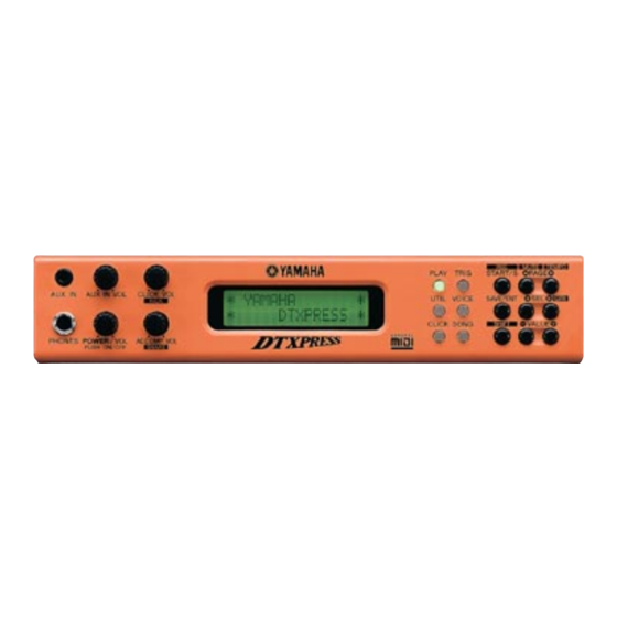
DTXPRESS PANEL LAYOUT Rear Panel 12 14 10 13 15 16 AUX IN Jack AUX IN Volume (AUX IN VOL) Head Phone Jack (PHONES) Power Switch/Master Volume (POWER/VOL) Click Volume (CLICK VOL) Accompaniment Volume (ACCOMP VOL) LCD Display Play Button (PLAY) -
Page 6: Circuit Board Layout
DTXPRESS CIRCUIT BOARD LAYOUT Chassis Unit CN204 CN203 CN202 CN201 Front Panel... -
Page 7: Block Diagram
DTXPRESS DTXPRESS BLOCK DIAGRAM IC11 CN401 IC209 IC12 IC205 IC203 IC209 IC14 CN203 CN204 CN401 PDT10 PORTC6 IC108 REPRESH PORTC1 SMA21 IC108 IC106 IC109 168P PDT8 IC109 IC106 IC13 24 32 IC101 VR101 CN502 IC10 IC110 CN501 IC501 SLIDE SWITCH... -
Page 8: Disassembly Procedure
DTXPRESS DTXPRESS DISASSEMBLY PROCEDURE Top Cover DM Circuit Board Assembly 1-1 Remove the five (5) screws marked [50]. The top 4-1 Remove the top cover. (See Procedure 1.) cover can then be removed. (Fig. 1) 4-2 Remove the front panel unit. (See Procedure 2.) 4-3 Remove the JK circuit board assembly. - Page 9 DTXPRESS Stay [6] x2 [5c] [4] x4 [9A] x2 [9B] x3 Panel stay Front panel [4]: Bind Head Tapping Screw-P 2.6X8 MFZN2Y (EP620100) [5c]: Bind Head Tapping Screw-B 3.0X6 MFZN2BL (EP600230) [6]: Bind Head Tapping Screw-B 2.6X8 MFZN2Y (EP620100) [9]: Bind Head Tapping Screw-P 2.6X8 MFZN2BL (EP620100)
-
Page 10: Lsi Pin Description
DTXPRESS LSI PIN DESCRIPTION HG73C205FD (XU947A00) SWX000 TONE GENERATOR DM IC001 NAME FUNCTION NAME FUNCTION Initial clear CMA3 Program address bus RFCLKI PLL Clock CMA8 Program address bus PLL Control CMA2 Program address bus AVDD_PLL Power supply read signal AVSS_PLL... -
Page 11: Ic Block Diagram
DTXPRESS DTXPRESS µPD63200GS-E1 (XP867A00) DAC (Digital to Analog Converter) DM IC007 NJM4556AMT1 (XQ138A00) SN75C1168NSR (XU073A00) TC74HC4052AF (XS790A00) NAME FUNCTION NAME FUNCTION Dual Operational Amplifier Line Driver Multiplexer DM IC108 DM IC10 AUX IC208,209 4/8FS 4/8 Fs selection R. REF Channel R voltage reference D. -
Page 12: Circuit Boards
DTXPRESS DTXPRESS CIRCUIT BOARDS DM Circuit Board MIDI to PN-CN401 9/10 to JK-CN202 HI HAT CONTROL to LCD UNIT HOST SELECT TO HOST to JK-CN203 OUTPUT L/MONO ACCOMP VOL DC IN 12V POWER/VOL PHONES Components side DM: ENA-V355530... - Page 13 DTXPRESS DTXPRESS DM Circuit Board DM: ENA-V355530 Pattern side...
- Page 14 DTXPRESS DTXPRESS JK Circuit Board to AUX-CN502 to DM-CN2 to DM-CN1 to DM-CN101 Components side INPUT 8 HI HAT 7 CRASH 6 RIDE 5 TOM3 4 TOM2 3 TOM1 2 SNARE 1 KICK ATTENUATION PN Circuit Board to DM CN4...
- Page 15 DTXPRESS DTXPRESS JK Circuit Board Pattern side AUX Circuit Board CLICK VOL to JK-CN204 AUX IN VOL to DM-CN102 AUX IN Components side Pattern side JK, AUX: ENA-V374810...
-
Page 16: Test Program
DTXPRESS DTXPRESS TEST PROGRAM A. How to enter the Program T–02. WAVE ROM Test No. Items Judgment Criteria While pressing the [PLAY] and [START/S] buttons turn Initial Display T–01. SRAM SRAM READ/WRITE (AutomaticTest) the power switch on. When the test program is initiated, T–02. - Page 17 Test End Test End OK: It proceeds to the next test automatically. Press the [SAVE/ENT.] button. The DTXPRESS will If an error is detected during the test, refer to section B, automatically proceed to the next test. [PROCEEDING THROUGH THE TEST].
- Page 18 DTXPRESS T–11. Panel Switch Result Screens Initial Display OK: It proceds to the next test automatically ATT. SW IN01 FAIL This test checks the panel switches. Press the panel switches one by one from [PLAY] to Test End [VALUE+] button in the order displayed on the LCD.
- Page 19 DTXPRESS Test End Result Screens OK: It proceeds to the next test automatically. OK: It proceeds to the next test automatically. If an error is detected during the test, refer to section B, [PROCEEDING THROUGH THE TEST]. HOST SELECT T–28. RIM SW IN 1: 1 KICK FAIL T–29.
- Page 20 DTXPRESS Test End T–41. OUTPUT R 10kHz OK: It proceeds to the next test automatically. Initial Display T–39. OUTPUT R 1kHz OUTPUT R 10kHz Initial Display 39 OUTPUT L 1kHz This test checks the OUTPUT (R) for the specified signal output level.
- Page 21 DTXPRESS This test checks the OUTPUT (R) for the specified signal Checks that the correct sine wave signals are output from output level. the unit. The signal from channels 1 to 16 is output from Insert the plugs into the OUTPUT (L/MONO and R) jacks.
- Page 22 DTXPRESS...
- Page 23 DTXPRESS...
- Page 24 DTXPRESS...
- Page 25 DTXPRESS...
- Page 26 DTXPRESS...
- Page 27 DTXPRESS...
- Page 28 DTXPRESS...
- Page 29 DTXPRESS...
-
Page 30: Midi Data Format
0 is the far left of a stereo image and 127 is the far right of a stereo image. When the [2-2. Channel 10 Propgram Change/Channel Event Receive] (P. 54) in the utility mode is set to “10PC=off”, the DTXPRESS will not receive MIDI 1.2.7 expression (No. - Page 31 F0 43 7D 0n ss ss 44 54 58 4C(“DTXL”) 53 59 53 54(“SYST”) Once active sensing data has been received, if no MIDI data is subsequently 00 00 7F 7F data csum F7 received for longer than an interval of approximately 300 msec, the DTXPRESS will mute all the sounds. 2.2.2 Send the messages within an interval of approximately 300 msec.
- Page 32 DTXPRESS...
- Page 33 DTXPRESS...
-
Page 34: Error Messages
Yamaha Service Center or the dealer where you purchased the device. The internal memory backup battery power is too low. User data may be deleted. WARNING Contact the nearest Yamaha Service Center or the dealer where you purchased Battery Low the device. - Page 35 DTXPRESS...
-
Page 36: Midi Implementation Chart
DTXPRESS YAMAHA [ Drum Trigger Module ] Date:5-Mar-1999 Model DTXPRESS MIDI Implementation Chart Version : 1.0 Transmitted Recognized Remarks Function ... Basic Default 1 - 16 1 - 16 memorized Channel Changed 1 - 16 1 - 16 Default Mode... -
Page 37: Parts List
DTXPRESS DRUM TRIGGER MODULE PARTS LIST CONTENTS OVERALL ASSEMBLY ………………………………………… 2 FRONT PANEL UNIT ………………………………………… 4 ELECTRICAL PARTS ………………………………………… 5 Notes: DESTINATION ABBREVIATIONS A :Australian model :Japanese model B :British model U :U.S. model C :Canadian model V :General export model (110V) - Page 38 DTXPRESS OVERALL ASSEMBLY 10 10c 10 10c...
- Page 39 DTXPRESS REF NO. PART NO. DESCRIPTION REMARKS QTY RANK OVERALL ASSEMBLY DTXPRESS J, U, C, N Overall Assembly (V360740) Sub Assembly (V360720) Front Panel Unit (V360700) Chassis Unit (V360710) E P 6 0 0 2 3 0 Bind Head Tapping Screw-B 3.0X6 MFZN2BL...
- Page 40 DTXPRESS FRONT PANEL UNIT 7b x9 REF NO. PART NO. DESCRIPTION REMARKS QTY RANK FRONT PANEL UNIT DTXPRESS Front Panel Unit (V360700) V 3 6 0 5 8 0 0 Front Panel Assembly V 3 6 1 0 8 0 0...
-
Page 41: Electrical Parts
DTXPRESS ELECTRICAL PARTS REF NO. PART NO. DESCRIPTION REMARKS QTY RANK ELECTRICAL PARTS DTXPRESS V 3 5 5 5 3 0 0 Circuit Board (XW047A0) V 3 5 5 5 5 0 0 Circuit Board (XW100A0) V 3 5 5 5 2 0 0... - Page 42 DTXPRESS REF NO. PART NO. DESCRIPTION REMARKS QTY RANK C0120 UB245100 Monolithic Ceramic Cap. F 0.100 25V Z C0121 UB052120 Monolithic Ceramic Cap. SL 120P 50V J C0122 UB052120 Monolithic Ceramic Cap. SL 120P 50V J C0123 UB245100 Monolithic Ceramic Cap.
- Page 43 DTXPRESS REF NO. PART NO. DESCRIPTION REMARKS QTY RANK IC014 XD599A00 TC74HC32F-T1 IC101 V R 9 0 3 7 0 0 Photo Coupler HCPL-M600 IC102 XM968B00 UPC24M09AHF REGULATOR IC103 XL497A00 UPC7805AHF REGULATOR +5V IC104 XT333A00 UPC29M33HF REGULATOR +3.3V IC105 XQ138A00...
- Page 44 DTXPRESS REF NO. PART NO. DESCRIPTION REMARKS QTY RANK R0106 RD256220 Carbon Resistor (chip) 2.2K 0.1 J R0107 RD257100 Carbon Resistor (chip) 10.0K 0.1 J -0109 RD257100 Carbon Resistor (chip) 10.0K 0.1 J R0110 RD256100 Carbon Resistor (chip) 1.0K 0.1 J...
- Page 45 DTXPRESS REF NO. PART NO. DESCRIPTION REMARKS QTY RANK TR105 V V 5 5 6 4 0 0 Transistor 2SC2412K Q,R,S TR106 V J 9 2 7 2 0 0 Transistor 2SA1162 O,Y TR107 V D 3 0 3 7 0 0...
- Page 46 DTXPRESS REF NO. PART NO. DESCRIPTION REMARKS QTY RANK R0209 RD255100 Carbon Resistor (chip) 100.0 0.1 J -0216 RD255100 Carbon Resistor (chip) 100.0 0.1 J R0217 RD258220 Carbon Resistor (chip) 220.0K 0.1 J -0220 RD258220 Carbon Resistor (chip) 220.0K 0.1 J...
- Page 47 DTXPRESS OVERALL CIRCUIT DIAGRAM KM23C16000C Shield Shield Shield S-DUS Power Supply Wave ROM 32M Wave ROM 16M DRAM 4M REGULATOR KEC-54187 µPC29M33HF (XT333A00) • REGULATOR +3.3V DIP Socket M5M51008CFP-70H-SR 1: INPUT 2: GND 3: OUTPUT SRAM 1M ASSP CONVERTER LINE...
Need help?
Do you have a question about the DTXPRESS and is the answer not in the manual?
Questions and answers