Table of Contents
Advertisement
Quick Links
Download this manual
See also:
User Manual
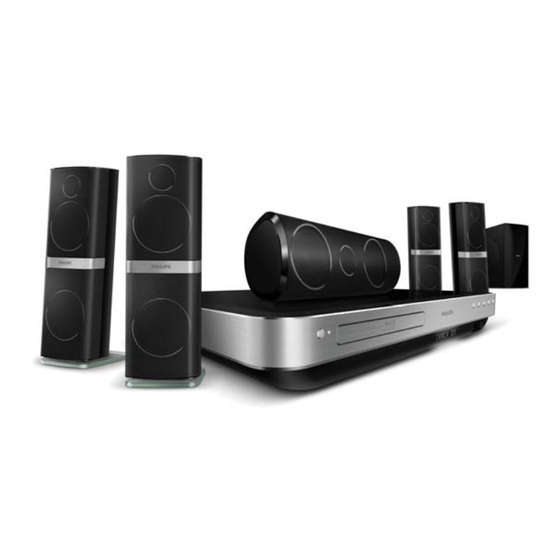
BD Home Theater System
Service
Service
Service
Service Manual
©
Copyright 2011 Philips Consumer Electronics B.V. Eindhoven, The Netherlands
All rights reserved. No part of this publication may be reproduced, stored in a retrieval system or
transmitted, in any form or by any means, electronic, mechanical, photocopying, or otherwise
without the prior permission of Philips.
Published by
RY_HY1130
Service Audio Printed in The Netherlands Subject to modification
Version 1.1
TABLE OF CONTENTS
Location Of PCB Boards............................................ 1-2
Versions Variation ...................................................... 1-2
Specifications ............................................................ 1-3
Measurement Setup .................................................. 1-6
Service Aids .............................................................. 1-7
ESD & Safety Instruction .......................................... 1-8
Lead-free Soldering Information ................................ 1-9
Setting Procedure & Repair Instructions ...................... 2
Disassembly Instructions & Service Positions .............. 3
Block & Wiring .............................................................. 4
Diagram Quick Strart Guide .......................................... 5
MAIN+VFD+USB&MP3+KARA+WILE+KEY+STBY Board
Power Board .................................................................. 7
BD Board........................................................................ 8
Mechanical Exploded View............................................ 9
Revision List ................................................................ 10
1 - 1
Chapter
.... 6
HTS8562/12/98
3139 785 35651
GB
Advertisement
Table of Contents

Related Manuals for Philips HTS8562/12


Summary of Contents for Philips HTS8562/12
- Page 1 Revision List ..............10 © Copyright 2011 Philips Consumer Electronics B.V. Eindhoven, The Netherlands All rights reserved. No part of this publication may be reproduced, stored in a retrieval system or transmitted, in any form or by any means, electronic, mechanical, photocopying, or otherwise without the prior permission of Philips.
-
Page 2: Location Of Pcb Boards
1 - 2 LOCATION OF PCB BOARDS WIRELESS PCB MAIN PCB BD PCB WIFI PCB KARAOKE PCB STANDBY PCB VFD PCB POWER PBC KEY PCB MP3&USB PCB VERSION VARIATION: Type/Versions HTS8562 HTS8562 Features Output Power - 1000W Voltage (220~240V) Ipod Dock Wireless ready SERVICE SCENARIO MATRIX: HTS8562... -
Page 3: Specifications
1 - 3 SPECIFICATIONS Video formats Media formats If you have a high definition TV, your home • AVCHD, BD, BD-R/ BD-RE, BD-Video, theater allows you to play your video files DVD-Video, DVD+R/+RW, DVD-R/- with: RW, DVD+R/-R DL, CD-R/CD-RW, • Resolution: 1920 x 1080 pixels at Audio CD, Video CD/SVCD, Picture files, •... - Page 4 1 - 4 .rm and .rmvb files in RM container (Available .mp4 or .m4v files in MP4 container only in Asia Pacific and China) Audio Video codec Bit rate Audio Video codec Bit rate codec codec Dolby MPEG 1, MPEG 2 20Mbps (peak AAC, RV30, 20Mbps (peak...
- Page 5 1 - 5 • Speaker drivers: 1 x 25.4 mm (1”) tweeter 2 x 76.2 mm (3”) woofer • Dimensions (WxHxD): 280 x 95 x 92mm • Compatibility: Hi-Speed USB (2.0) • Weight: 1.40kg • Classsupport: USB MassStorage Class • Cable length: 2m (MSC) Front / rear speakers:...
- Page 6 1 - 6 MEASUREMENT SETUP Tuner FM Bandpass LF Voltmeter 250Hz-15kHz e.g. PM2534 e.g. 7122 707 48001 RF Generator e.g. PM5326 S/N and distortion meter e.g. Sound Technology ST1700B Use a bandpass filter to eliminate hum (50Hz, 100Hz) and disturbance from the pilottone (19kHz, 38kHz). Use Audio Signal Disc SBC429 4822 397 30184 (replaces test disc 3)
- Page 7 1 - 7 SERVICE AIDS Service Tools: Universal Torx driver holder .........4822 395 91019 Torx bit T10 150mm ...........4822 395 50456 Torx driver set T6-T20 .........4822 395 50145 Torx driver T10 extended ........4822 395 50423 Compact Disc: SBC426/426A Test disc 5 + 5A ......4822 397 30096 SBC442 Audio Burn-in test disc 1kHz ....4822 397 30155 SBC429 Audio Signals disc .........4822 397 30184 Dolby Pro-logic Test Disc ........4822 395 10216...
- Page 8 1 - 8 WAARSCHUWING WARNING Alle IC’s en vele andere halfgeleiders zijn All ICs and many other semi-conductors are gevoelig voor electrostatische ontladingen susceptible to electrostatic discharges (ESD). (ESD). Careless handling during repair can reduce life Onzorgvuldig behandelen tijdens reparatie kan drastically.
- Page 9 • You will find this and more technical information Use only lead-free solder alloy Philips SAC305 with within the “magazine”, chapter “workshop news”. order code 0622 149 00106. If lead-free solder-paste is required, please contact the manufacturer of your For additional questions please contact your local solder-equipment.
- Page 10 For more information,frequently asked questions and version of your home theater with the latest software version (if software updates,please visit available) on the Philips web site, and for BD-Live application and Software BE philips.com/support software update, make sure that the network router has access to the Internet and the firewall is disabled.
- Page 11 2 - 2 2 - 2 c) Assembly Blu-ray Loader to “J800”,”J900”,”J905” on the top of Software upgrade will take 5 minutes BD Board as shown below. Do not switch off! Package version: 000025.0 Software BE Completed Software FE Completed Software MCU1: Not started Software Dock:...
- Page 12 2 - 3 2 - 3 REPAIR INSTRUCTIONS MAIN UNIT REPAIR CHART Al l Function No Working All Function No Sound AUX IN No Sound MP3 IN No Sound TUNE R Function No Sound Coaxial in Function No Sound Optical In No Sound Dock In No Sound US B No Function WI FI No Function...
- Page 13 3 - 1 3 - 1 DISASSEMBLY INSTRUCTIONS Dismantling of Blu-ray Loader 1) Loosen 4 screws “ C “ at the Blu-ray Loader as shown in fi gure 6. Dismantling of the Top panel 1) Loosen 11 screws to remove the Top Cover . - 5 screws “A”...
- Page 14 3 - 2 3 - 2 Dismantling of the Main Board Dismantling of the Power Board 1) Loosen 3 screws “E” on the top of Main Board as shown in fi gure 8. 1) Loosen 5 screws “G” on the top of Power Board as shown in fi gure 12. 2) Loosen 8 screws “F”...
-
Page 15: Service Positions
3 - 3 3 - 3 Dismantling of the MP3+USB Board SERVICE POSITIONS 1) Remove the Display Lens as shown in fi gure 16. Service Position A - MAIN Board Service Position B - POWER Board 2) Loosen 2 screws “K” on the top of MP3&USB board as shown in fi gure 17. Figure 16 Service Position C - MAIN &... - Page 16 4 - 1 4 - 1 BLOCK DIAGRAM...
- Page 17 4 - 2 4 - 2 WIRING DIAGRAM...
- Page 18 QUICK START GUIDE The following excerpt of the QSG/DFU serves as an introduction to the set. The complete Direction for Use can be download in the different languages from the internet site of Philips Consumer Care Center:www.support.philips.com. SUB- SUB- FRONT...
- Page 19 5 - 2 5 - 2 MUSIC iLINK HDMI OUT (ARC) HDMI IN HDMI IN HDMI OUT (ARC) TO TV TO TV HDMI IN / HDMI (ARC) AC MAINS~ FRONT FRONT FRONT REAR REAR SUB- RIGHT LEFT CENTRE RIGHT LEFT WOOFER HDMI OUT COAXIAL...
- Page 20 5 - 3 5 - 3 HDMI MUSIC iLINK MUSIC iLINK SUB- FRONT FRONT WOOFER FRONT LEFT RIGHT CENTER HOME THEATER HOME THEATER REAR REAR LEFT RIGHT...
- Page 21 5 - 4 5 - 4 MUSIC iLINK MUSIC DOCK for iPod iLINK HOME THEATER...
-
Page 22: Table Of Contents
6 - 1 6 - 1 INTERNAL IC DIAGRAM - CS495313-CVZ Paral i el Ser i al Ser i al D eoug Cont r ol U ART G PIO Cont r ol 1 Cont r ol 2 12Ch,Audio In/ 6Ch,SACD In MAIN+VFD+USB&MP3+KARA+WILE+KEY+STBY BOARD 32-b it 32-b it... -
Page 23: Circuit Diagram(Part One)
6 - 2 6 - 2 CIRCUIT DIAGRAM(part one) C5001 C5093 C5189 R5050 C5002 C5094 C5190 R5051 C5003 C5095 C5191 R5053 JK 5001B JK 5001A C5004 C5096 C5192 R5054 JK _SP_6C H_CJ S003021-0010_0020 C5005 C5097 C5193 R5055 C5006 C5098 C5194 R5056 CJS 003021-0010 CJS 003021-0020... -
Page 24: Circuit Diagram(Part Two)
6 - 3 6 - 3 CIRCUIT DIAGRAM(part two) C001 R319 C301 R320 C302 R321 KE Y SW _1 0.6V C303 R322 R 850 R 851 R 852 R 853 R 854 Q850 C304 R323 0.35V 0.69V 0.99V 1.3V 1.63V RB104 2SA733 C307... -
Page 25: Circuit Diagram(Part Three)
6 - 4 6 - 4 CIRCUIT DIAGRAM(part three) C3000 C3020 C3038 C3057 C3075 C3095 C3113 C3134 C3154 C3176 C370 D3003 L3001 R3006 R3024 R3042 R3061 R3080 R3101 R3125 R3145 R3163 R395 C3001 C3021 C3039 C3058 C3076 C3096 C3114 C3135 C3155 C3177 C371... -
Page 26: Circuit Diagram(Part Four)
6 - 5 6 - 5 CIRCUIT DIAGRAM(part four) C100 A3 FB113 D4 R188 A2 C101 C3 IC101 A2 R189 A2 C102 C3 IC103 B3 R190 A2 C103 D3 IC103 B3 R192 A2 2K 7 100K R1002 HPD_5V R112 R190 ED ID_PWR C104 C2 IC104 C3... -
Page 27: Circuit Diagram(Part Fi Ve)
6 - 6 6 - 6 CIRCUIT DIAGRAM(part fi ve) C1003 C205 C214 C223 FB203 Q1006 R1055 R201 R209 R216 R223 R231 R239 R246 R253 R260 R268 R277 R285 R293 XL200 C1004 C206 C215 C224 FB204 Q200 R200 R202 R210 R217 R224 R232... -
Page 28: Circuit Diagram(Part Six)
6 - 7 6 - 7 CIRCUIT DIAGRAM(part six) C801 C805 C810 C814 C819 C823 C827 CN804 D804 Q801 R801 R806 R810 R816 R820 R824 R828 ZD801 C802 C806 C811 C815 C820 C824 CN801 D801 DP801 Q802 R802 R807 R811 R817 R821 R825... -
Page 29: Pcb Layout Top View
6 - 8 6 - 8 PCB LAYOUT - TOP VIEW C100 C3017 C3101 C3165 C5048 C5084 C5120 C5175 CN305 C4 FB103 IC104 L3003 Q302 R114 R180 R217 R257 R3001 R3035 R3072 R3137 R3180 R5044 R5083 R5135 TA100 C1004 C3018 C3102 C3167 C5049... -
Page 30: Pcb Layout Bottom View
6 - 9 6 - 9 PCB LAYOUT - BOTTOM VIEW C001 C122 C189 C3003 B1 C3026 A2 C3045 A1 C3065 B3 C3106 B2 C3147 A2 C3186 B3 C375 C5016 A4 C5034 B4 C5165 B3 C803 D5007 A3 Q3007 A2 R183 R298 R3098 B2... - Page 31 7 - 1 7 - 1 INTERNAL IC DIAGRAM - AZ431 CATHODE POWER BOARD ANODE TABLE OF CONTENTS Internal IC Diagram ................7-1 Circuit Diagram .................. 7-2 PCB Layout Top View ............... 7-3 PCB Layout Bottom View ..............7-4 INTERNAL IC DIAGRAM - SSC620S SOP...
- Page 32 7 - 2 7 - 2 CIRCUIT DIAGRAM BD901 C925 C949 C961 C970 C986 CE901 CY902 D911 D934 L905 Q904 Q995 R915 R928 R934 R945F R948 R964 R976 R990 T903 ZD908 C902 C927 C950 C962 C971 C990 CE902 CY903 D912 F901 L906 Q906...
- Page 33 7 - 3 7 - 3 PCB LAYOUT - TOP VIEW BD901 C915 C961 C968 C974 CE902 CN906 D904 D923 GT903 J903 J911 J918 J925 L904 LF902 Q910 R936 R996 TVR901 D1 C901 C923 C962 C969 C978 CE902 CX901 D907 D924 GT904 J904...
- Page 34 7 - 4 7 - 4 PCB LAYOUT - BOTTOM VIEW C903 C928 C948 C964 C991 D902 D913 IC903 Q915 R905 R916 R925 R930E R937 R945D R945L R952 R961 R970 R979 R988 R999 ZD907 C913 C929 C949 C967 C991A D903 D914 Q904 Q917...
- Page 35 8 - 1 8 - 1 BLOCK DIAGRAM BD BOARD TABLE OF CONTENTS Block Diagram(BD Board) ..............8-1 Voltages for connector pin ..............8-2 Waveforms for measure point ............8-3...
- Page 36 8 - 2 8 - 2 Voltages for per connection pin 5. J800--->>from BD board connect to BD loader(SERVO use) 1. HA500--->>from BD board connect to main board 2. CN202--->>from BD board connect to USB connect PCB PIN NO PIN Assign Remarks PIN NO PIN Assign...
- Page 37 8 - 3 8 - 3 Waveforms for measure point HA500 PIN10_MIC_IN HA500 PIN9_CEC(no single) HA500 PIN2_Ipod_TX HA500 PIN3_Ipod_RX Disc function wave Play BD Disc wave Play BD Disc wave HA500 PIN12_SCL HA500 PIN13_SDA HA500 PIN5_12C_IRQ HA500 PIN7_IR(VOL up/down) Play BD Disc wave Play BD Disc wave Play BD Disc wave Play BD Disc wave...
- Page 38 8 - 4 8 - 4 Waveforms for measure point HA500 PIN19_BCK HA500 PIN21_AOSDAT0 CN203 Pin3 USBM pin4 USBP Play BD Disc wave Play BD Disc wave USB and WIFI Function wave HA500 PIN22_AOSDAT1 HA500 PIN23_AOSDAT2 Play BD Disc wave Play BD Disc wave HA500 PIN29_HDMI_ARC HA500 PIN10_A_MUTE...
- Page 39 9 - 1 9 - 1 Mechanical Exploded View Note:A1=3+5+8+24+29+33+36...
- Page 40 10- 1 REVISION LIST Version 1.0 *Initial release Version 1.1 *HTS8562/12 combine with HTS8562/98...
Need help?
Do you have a question about the HTS8562/12 and is the answer not in the manual?
Questions and answers