Table of Contents
Advertisement
Quick Links
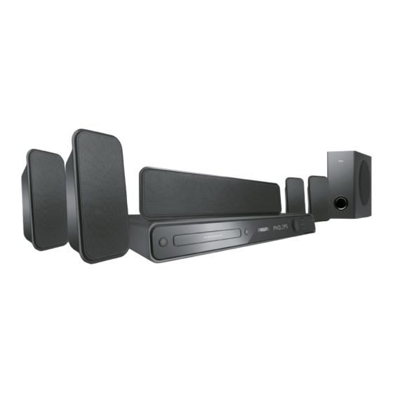
DVD Home Theater System
Service
Service Manual
©
Copyright 2008 Philips Consumer Electronics B.V. Eindhoven, The Netherlands
All rights reserved. No part of this publication may be reproduced, stored in a retrieval system or
transmitted, in any form or by any means, electronic, mechanical, photocopying, or otherwise
without the prior permission of Philips.
Published by
LM0810
Service Audio Printed in The Netherlands Subject to modification
Version 1.0
TABLE OF CONTENTS
Location of PCB Boards .............................................. 1-2
Versions Variation ....................................................... 1-2
Specifications .............................................................. 1-3
Measurement setups ................................................... 1-4
Service Aids................................................................. 1-5
ESD & Safety instruction ............................................. 1-6
Lead-tree solding information ...................................... 1-7
Setting procedure & Repair instructions ......................... 2
Disassembly instruction & Service Postion .................... 3
Block & Wring Diagram .................................................. 4
VFD+JACK+VOL+STANDBY Board .............................. 5
Main Board ..................................................................... 6
Power Board................................................................... 7
AMP Board ..................................................................... 8
Mechanical Exploded View & Parts................................ 9
Revision List ................................................................. 10
1 - 1
Chapter
HTS3565/98/HTS3568/98
GB
3139 785 33620
Advertisement
Table of Contents

Related Manuals for Philips HTS3565/98


Summary of Contents for Philips HTS3565/98
- Page 1 Revision List ..............10 © Copyright 2008 Philips Consumer Electronics B.V. Eindhoven, The Netherlands All rights reserved. No part of this publication may be reproduced, stored in a retrieval system or transmitted, in any form or by any means, electronic, mechanical, photocopying, or otherwise without the prior permission of Philips.
-
Page 2: Location Of Pcb Boards
1 - 2 LOCATION OF PCB BOARDS MAIN PCB AMP PCB STANDBY PCB VFD PCB Power PCB VOL PCB JACK PCB VERSION VARIATION: HTS3569 Type/Versions HTS3565 Features Main(Power Output-1000W) S-video out Power Voltage (120V/230V) SERVICE SCNARIO MATRIX: Type/Versions HTS3565 HTS3569 Boards in used Main Board Power Board... - Page 3 1 - 3 SPECIFICATIONS (red colour only for hts3569/98) FRONT AND REAR SPEAKERS AMPLIFIER Total output power System ............Full range satellite Impedance ............... 6 ohm Home Theatre mode ............1000W Speaker drivers ........3” full range speaker Frequency response ......180 Hz~18 kHz / ±3dB Signal-to-noise ratio ........
- Page 4 1 - 4 MEASUREMENT SETUP Tuner FM Bandpass...
- Page 5 1 - 5...
- Page 6 1 - 6...
- Page 7 1 - 7...
- Page 8 “ok” button to con rm * the system will switch off and on again automatically. c) TV will show message as below: e) OSD will show: Current model HTS3565/98 HTS3569/98 Version: 00.12.01_1 Release: 2007.12.19 upgrade le detected region Servo: 5B.61.00.00...
- Page 9 2 - 2 2 - 2 REPAIR INSTRUCTIONS (part one)
- Page 10 2 - 3 2 - 3 REPAIR INSTRUCTIONS (part two)
- Page 11 2 - 4 2 - 4 REPAIR INSTRUCTIONS (part three)
-
Page 12: Dismantling Of The Amp Board
3 - 1 3 - 1 DISASSEMBLY INSTRUCTIONS Dismantling of the Front Panel Assemble 3) Loosen 7 screws and remove the Top Cover by lifting the rear portion upwards before sliding it out towards the rear. - 1 screw “A” each on the left & right side as shown in gure 4 1) Open the DVD Tray by using the Open/Close Button while the Set is ON and disconnect the mains supply after removing the Tray - 5 screws “B”... -
Page 13: Vfd+Jack+Vol+Standby Board
3 - 2 3 - 2 Dismantling of the Main Board Dismantling of the VFD+JACK+VOL+STANDBY Board 1) Loosen 2 screws “ G “ on the top of main board as shown in gure10 1) Loosen 9 screws “J” on the top of control board as shown in 13 2) Loosen 7 screws “H”... - Page 14 4 - 1 4 - 1 BLOCK DIAGRAM...
- Page 15 4 - 2 4 - 2 WIRING DIAGRAM AMP PCB MAIN PCB TUNER POWER PCB DVD LOADER CONTROL PCB...
- Page 16 5 - 1 5 - 1 FTD DISPLAY PIN ASSIGNMENT CONTROL BOARD TABLE OF CONTENTS FTD Display Pin Assignment ............. 5-1 Circuit Diagram ................. 5-2 PCB Layout Top & Bottom View ............5-3 PIN CONNECTION...
- Page 17 5 - 2 5 - 2 CIRCUIT DIAGRAM FB11 FB17 RB14 SN11 TA18 CN12 FB12 IC11 RB15 TA11 TA19 FB13 JK11 RB16 TA12 TA20 FB14 JK12 RB11 RB17 TA13 USB11 D3 FB15 LD11 RB12 RB18 TA14 VR11 DP11 FB16 RB13 RB19 TA15...
- Page 18 5 - 3 5 - 3 PCB LAYOUT - TOP VIEW CN12 A2 JK11 A4 RB14 A1 RB18 A4 TA12 A1 TA18 A4 VR11 A3 JK12 A4 RB11 A1 RB15 A4 RB19 A4 TA13 A4 TA19 A4 LD11 A1 RB12 A1 RB16 A4 SN11 A1 TA14 A1...
-
Page 19: Table Of Contents
6 - 1 6 - 1 INTERNAL IC DIAGRAM - AS81F641642C MAIN BOARD TABLE OF CONTENTS Internal IC Diagram ................6-1 Circuit Diagram (part one) ..............6-2 INTERNAL IC DIAGRAM - MT1389E Circuit Diagram (part two) ..............6-3 PCB Layout Top View ..............6-4 PCB Layout Bottom View .............. - Page 20 6 - 2 6 - 2 CIRCUIT DIAGRAM - part one C301 A1 C902 D1 D302 D4 R337 D4 C302 A1 C903 D1 D303 D4 R338 D5 C305 A2 C904 D1 FB310 A4 R340 D4 C306 A1 C905 D1 FB311 D3 R341 D4 C309 A2 C906 D2...
- Page 21 6 - 3 6 - 3 CIRCUIT DIAGRAM - part two C0201 C2 C242 B3 CE203 D2 IC202 C5 R237 A3 C0202 A3 C243 D3 CE204 D2 IC203 D3 R238 D5 C0203 A3 C253 C2 CE205 D2 IC204 D3 R239 D4 C0204 D1 C254 D3 CE206 D2...
- Page 22 6 - 4 6 - 4 PCB LAYOUT - TOP VIEW C0202 A3 C601 A2 CN207 C4 L204 A3 R286 B4 R518 C5 C0207 C2 C602 A2 CN208 C3 L205 A2 R287 B4 R519 C5 C0208 C3 C701 A3 CN301 B1 L206 B2 R290 C3 R520 C5...
- Page 23 6 - 5 6 - 5 PCB LAYOUT - BOTTOM VIEW C0201 B4 C324 B2 CE220 B5 FB707 B4 C0203 B4 C358 C1 CE301 C4 FE301 B4 C0204 B4 C502 B1 CE302 C4 FE302 B4 C0205 C5 C503 B1 CE303 C4 FE303 A4 C0206 B5 C506 C1...
-
Page 24: Internal Ic Diagram
7 - 1 7 - 1 INTERNAL IC DIAGRAM - AP3843GMTR POWER BOARD TABLE OF CONTENTS Internal IC Diagram ................7-1 Circuit Diagram .................. 7-2 PCB Layout Top View ............... 7-3 INTERNAL IC DIAGRAM - KA7500C PCB Layout Bottom View ..............7-4 OUTPUT CONTROL OSCILLATOR DEAD... -
Page 25: Circuit Diagram (Part One)
7 - 2 7 - 2 CIRCUIT DIAGRAM BD901 A1 C915 A3 C927 B3 C941 B2 C954 B3 C964A C1 C978 C2 D907 A4 D920 B2 IC904 C2 NTC901 C1 Q917 C4 R910 A3 R926A A4 R938 B2 R953 B1 R967 B2 R981 C2 R995 C4... - Page 26 7 - 3 7 - 3 PCB LAYOUT - TOP VIEW BD901 A1 C921 C946 C962 CN901 A1 D917 D937 J909 J918 J929 L903 Q910 R905 R940 R964 T901 C901 C922 C949 C963 CN903 A4 D918 GT901 B1 J910 J920 J930 L904 Q911...
- Page 27 7 - 4 7 - 4 PCB LAYOUT - BOTTOM VIEW C904 C919 C930 C948 C964A C3 D901 D916 R901 R921 R926D B1 R950 R962 R976 R989 ZD905 B1 C906 C923 C931 C954 C964B C3 D905 D991 R902 R922 R927 R951 R967 R977...
-
Page 28: Amp Board
8 - 1 8 - 1 INTERNAL IC DIAGRAM - CO4558A SO8 VCC+ AMP BOARD TABLE OF CONTENTS Internal IC Diagram ................8-1 VCC- Circuit Diagram .................. 8-2 PCB Layout Top view ............... 8-3 PCB Layout Bottom View ..............8-4... -
Page 29: Circuit Diagram (Part Two)
8 - 2 8 - 2 CIRCUIT DIAGRAM C463 C2 C536 D2 L403 R448 C2 C464 C2 C537 D2 L404 R449 C3 C465 C2 C538 D2 L405 R450 C3 C466 C3 C539 D2 L406 R451 D3 C467 C3 C540 D2 L407 R452 D3 C468 B1... -
Page 30: Pcb Layout Top View
8 - 3 8 - 3 PCB LAYOUT - TOP VIEW C520 C602 C510 C428 C521 FB401 A4 IC403 JK401 D4 C522 IC404 R408 L401 C523 Q412 R409 L402 R510 R401 R485 RB401 A1 R402 R486 ZD415 A1 R403 C443 R404 C505 R405... -
Page 31: Pcb Layout Bottom View
8 - 4 8 - 4 PCB LAYOUT - BOTTOM VIEW CE404 C1 R466 CE405 B1 R467 C401 CE406 C1 R472 C402 CE407 D1 R479 C403 CE408 D1 R509 C404 CE409 C1 R511 C405 CE410 C1 R515 C406 CE411 D1 R522 C407 CE412 D1... - Page 32 9 - 1 9 - 1 MECHANICAL EXPLODED VIEW A1=14+15+36+38...
- Page 33 9 - 2 9 - 2 MECHANICAL PART LIST(red colour only for hts3569/98) RFFR 996510010854 RUBBER FOOT -CENTER F901 994000001053 FUSE 6.3A 250V Loc. 12NC. Description 996510013306 RUBBER FOOT -SUB IC901 996510008293 IC 16P AZ7500BP-E1 SPKC 996510013300 SPEAKER BOX -CENTER IC902 996510004113 IC 8P AP3843GMTR-E1...
- Page 34 9 - 3 9 - 3 IC301 996500041286 IC 8P 4558 994000000915 XISTR NPN 2SC1623 JK401 996510012528 SPKJACK6P IC303 996500029611 IC 8P CO4558A SO8 994000000921 XISTR PNP 2SA812 HFE:200-400 996510013837 SPK JAC12p JK401&401A IC303 996500041286 IC 8P 4558 994000000921 XISTR PNP 2SA812 HFE:200-400 JK401A 996510012529 SPKJACK 6...
-
Page 35: Revision List
10 - 1 10 - 1 REVISION LIST Version 1.0 *Initial release...
Need help?
Do you have a question about the HTS3565/98 and is the answer not in the manual?
Questions and answers