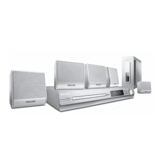
Philips HTS3000/98 Service Manual
Hide thumbs
Also See for HTS3000/98:
- Quick start manual (2 pages) ,
- User manual (47 pages) ,
- Service manual (31 pages)

Related Manuals for Philips HTS3000/98


Summary of Contents for Philips HTS3000/98
- Page 1 Chapter 3139 785 32752 0749...
- Page 2 TUNER PCB STANDY PCB MAIN PCB POWER PCB CONTROL PCB VOL PCB...
-
Page 3: Speci Cations
Speci cations AMPLIFIER FRONT AND REAR SPEAKERS Total output power System: ............Full range satellite -Home Theater Mode: ............ 200 W Impedance: ................4 Frequency Response: ....... 180 Hz – 18 kHz / ±3 dB Speaker drivers: ........3” full range speaker Signal-to-Noise Ratio: ......>... - Page 4 Measurement Setup Tuner FM Bandpass Tuner AM (MW,LW) Bandpass...
- Page 5 SERVICE AIDS Service Tools: Universal Torx driver holder .........4822 395 91019 Torx bit T10 150mm ...........4822 395 50456 Torx driver set T6-T20 .........4822 395 50145 Torx driver T10 extended ........4822 395 50423 Compact Disc: SBC426/426A Test disc 5 + 5A ......4822 397 30096 SBC442 Audio Burn-in test disc 1kHz ....4822 397 30155 SBC429 Audio Signals disc .........4822 397 30184 Dolby Pro-logic Test Disc ........4822 395 10216...
- Page 6 WAARSCHUWING WARNING Alle IC’s en vele andere halfgeleiders zijn All ICs and many other semi-conductors are gevoelig voor electrostatische ontladingen susceptible to electrostatic discharges (ESD). (ESD). Careless handling during repair can reduce life Onzorgvuldig behandelen tijdens reparatie kan drastically. de levensduur drastisch doen verminderen. When repairing, make sure that you are Zorg ervoor dat u tijdens reparatie via een connected with the same potential as the mass...
- Page 7 Due to lead-free technology some rules have to be Philips-sets respected by the workshop during a repair: You will find this and more technical information Use only lead-free solder alloy Philips SAC305 with • within the “magazine”, chapter “workshop news”. order code 0622 149 00106. If lead-free solder-paste...
- Page 8 2 - 1 2 - 1 System , Region Code , etc. Setting Produre 1)System Reset 6)Produce to Change Tuner Grid (only applicable for certain regions) a) press “system “ button on R/C,TV show “setup“ b) select the menu using the on R/C In some countries ,the frequency step between adjacent channels c) go preference page to do sysytem reset...
- Page 9 2 - 2 2 - 2 REPAIR INSTRUSTRATOR Chang F901 Ok or No Check CHANG D902/903/904/908 D902/903/904/908 D909/911/912 D909/911/912 OK or No Check Repair IC901/IC902/IC903 /Q902 or output circuit...
- Page 10 3 - 1 3 - 1 Dismantling of the Main PCB DISASSEMBLY INSTRUCTIONS 2) Return the set to its upright position and remove the Tray Cover as shown in Figure 3 and close the tray manually by 1) Loosen 4 screw “ A “ on the top of main board as shown in pushing it back in.
- Page 11 top of control board...
- Page 12 4 - 1 4 - 1 BLOCK DIAGRAM...
- Page 13 4 - 2 4 - 2 WIRING DIAGRAM...
- Page 14 5 - 1 5 - 1 FTD DISPLAY PIN ASSIGNMENT CONTROL BOARD TABLE OF CONTENTS FTD Display Pin Assignment ............. 5-1 Voltage ....................5-2 Circuit Diagram .................. 5-3 PCB Layout Top & Bottom View ............5-4...
- Page 15 5 - 2 5 - 2 VOLTAGE Q200 Pin NO Voltage -0.9 Pin NO Voltage -18.9 -25.3 -25.3 -25.3 -25.3 -16.4 23.2 Pin NO Voltage -18.6 -1836 -20.8 -25.3 -25.3 -16.5 -18.7 -16.5 -25.4 -25.4 23.2 -25.7 -23.2 -23.2 -23.2 -23.2 -23.2 -23.2 Pin NO Voltage -23.2 -23.2 -23.2 -23.2...
- Page 16 5 - 3 5 - 3 CIRCUIT DIAGRAM C200 C204 C208 C212 C216 C220 C288 D202 IC200 B1 R201 R205 R209 R213 R218 RB200A A4 TA200 C1 TA204 C1 ZD200 A2 ZD204 A3 C201 C205 C209 C213 C217 C221 C289 D203 LD200 C4 R202...
- Page 17 5 - 4 5 - 4 PCB LAYOUT - TOP VIEW C208 D202 JW12 JW18 R211 RB204 TA204 C209 D203 JW13 JW19 LD200 R213 SN200 TA205 C216 DP200 JW14 R200 R214 TA200 VR200 CN203 JW15 JW20 R201 R215 TA201 XL200 D200 JW10 JW16...
- Page 18 6 - 1 6 - 1 INTERNAL IC DIAGRAM - CO4558A SO8 MAIN BOARD TABLE OF CONTENTS Internal IC Diagram ................6-1 Circuit Diagram .................. 6-2 PCB Layout Top View ............... 6-3 PCB Layout Bottom View ..............6-4 Voltage ....................6-5 INTERNAL IC DIAGRAM - V5888S HOSP MUTE BLAS...
- Page 19 6 - 2 6 - 2 Circuit Diagram C1001 D3 C182 C441 C829 IC105 R158 R519 C830 IC302 R159 R520 C1002 D3 C183 C502 C1003 D3 C184 C504 C831 IC303 R160 R521 C1004 D3 C185 C505 C833 IC304 R162 R522 C1005 D3 C186 C506...
- Page 20 6 - 3 6 - 3 PCB Layout Top View C1111 FB125 A1 R152 C126 IC303 R325 RA101 A2 C414 Q301 R407 JK501A A4 C805 C836 Q104 R823 C165 D108 Q103 R819 C551 ZD104 B3 C567 C129 FB126 A1 R153 C323 IC304 R326...
- Page 21 6 - 4 6 - 4 PCB Layout Bottom View C193 A1 R506 A1 R526 A1 C404 A2 C427 A2 C301 A3 R124 A3 C1101 A4 C1113 A4 R1103 A4 C431 B1 C573 B1 C180 B2 C546 B2 C1007 B3 C127 B3 C856 B3 R3012 B3...
- Page 22 6 - 5 6 - 5 Voltage Q101 Q102 Q103 Q104( 2SC945P) Pin NO Pin NO Pin NO Pin NO Pin NO Voltage Voltage Voltage Voltage Voltage Pin NO Voltage Pin NO Q110 Q1101 Q1102 Q1103 Voltage Pin NO Pin NO Pin NO Pin NO Pin NO...
- Page 23 7 - 1 7 - 1 VOLTAGE Pin NO Voltage Pin NO Voltage Pin NO Voltage Pin NO Voltage POWER BOARD Q901 Q902 Q903 Q904 Pin NO Pin NO Pin NO Pin NO Voltage 30.5 31.6 Voltage -2.3 165.4 Voltage 33.3 -2.7 Voltage...
- Page 24 7 - 2 7 - 2 CIRCUIT DIAGRAM BD901 A1 C909 C917 C925 C933 C941 CN901 A4 D904 D914 IC904 Q902 R901 R909 R917 R925 R934 R943 R952 C901 C910 C918 C926 C934 C942 CN902 A4 D905 F901 L901 Q903 R902 R910 R918...
- Page 25 7 - 3 7 - 3 PCB LAYOUT - TOP VIEW BD901 C910 C921 C928 C940 C950 D901 D909 GT902 J905 J912 L905 Q905 R905 R929 TVR901 B1 C901 C911 C923 C929 C941 CN901 D902 D911 GT903 J906 J913 NTC901 B1 Q906 R908 R932...
- Page 26 7 - 4 7 - 4 PCB LAYOUT - BOTTOM VIEW C904 C914 C922 C935 C945 J901 R904 R910 R914 R921 R926 R931 R937 R945 R949 ZD901 C905 C915 C931 C937 D910 J903 R906 R911 R917 R923 R927 R934 R941 R946 R951 C908...
- Page 27 Note: A1=16+15+11...
- Page 28 Note: A1=16+15+11...
- Page 29 (for: /51/94/98) (for: /55) 996510007283 SHEET 996510007285 (for: /51) (for: /55/94/98)
Need help?
Do you have a question about the HTS3000/98 and is the answer not in the manual?
Questions and answers