Table of Contents
Advertisement
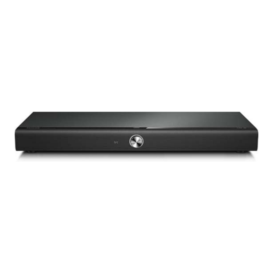
Sound Stage
Service
Service Manual
. Location of PCB Boards,Version Variation and Repair Scenario Matrix.....1-2
. Technical Specifications.........................................................1- 3
. Safety Instruction, Warning & Notes........................................1- 4
. DFU Instruction..............................................................................2-1
. Mechanical and Dismantling Instructions....................................3-1
. Software Upgrades .......................................................................
. Trouble Shooting Chart......................................................
. Wiring Diagram..................................................................6-1
. Electrical Diagrams and Print-layouts......................................7-1
. Pin Description & Block Diagrams of ICs..................................8-1
. Set Mechanical Exploded view & Part list...............................9-1
. Revision List.................................................................................10-1
©Copyright 2013 Philips Consumer Electronics B.V. Eindhoven, The Netherlands
All rights reserved. No part of this publication may be reproduced, stored in aretrieval system or
transmitted, in any form or by any means, electronic, mechanical, photocopying, or otherwise
without the prior permission of Philips.
Published by Arya & Stephen - 1338 Printed in The Netherlands Subject to modification
Version 2.0
TABLE OF CONTENTS
HTL4111B/12
Page
4-1
.
5-1
.
GB
3142 038 61020
PHILIPS
Advertisement
Table of Contents

Subscribe to Our Youtube Channel
Related Manuals for Philips HTL4111B/12


Summary of Contents for Philips HTL4111B/12
-
Page 1: Table Of Contents
. Set Mechanical Exploded view & Part list.…………………..….…9-1 . Revision List.................10-1 ©Copyright 2013 Philips Consumer Electronics B.V. Eindhoven, The Netherlands All rights reserved. No part of this publication may be reproduced, stored in aretrieval system or transmitted, in any form or by any means, electronic, mechanical, photocopying, or otherwise without the prior permission of Philips. - Page 2 PCB Board Locations PCB Board Locations USB&MP3 BOARD NFC BOARD Top Side FRONT CONTROL BOARD KEY BOARD POWER BOARD MAIN BOARD Bottom Side Reminder: As BT and NFC need to be paired , and BT is on FE board , when one of BT , NFC or FE Board needs to be replaced , all of these three parts need to be replaced together.
-
Page 3: Specifications
Version: Product WMA: V7, V8, V9 specifications Bluetooth Bluetooth version: 2.1 + EDR Note Main unit notice. Power supply: 110-240 V~, 50/60 Hz Power consumption: 80 W Speaker impedance: 4 ohm Speaker drivers: 2 x racetrack mid range Total output power: 120W RMS (+/- 0.5 (1.5"... -
Page 4: Safety Instruction, Warning & Notes
Safety instruction, Warning & Notes Safety instruction 1. General safety 2.Laser safety Safety regulations require that during a repair: This unit employs a laser. Only qualified service personnel . Connect the unit to the mains via an isolation transformer. may remove the cover, or attempt to service this device . - Page 5 Warning 1.General 2. Laser . All ICs and many other semiconductors are susceptible to . The use of optical instruments with this product, will electrostatic discharges (ESD). Careless handing during increase eye hazard. repair can reduce life drastically. Make sure that, during .
- Page 6 Solder Joint...
- Page 7 - lead free BGA-ICs will be delivered in so-called respected by the workshop during a repair: ‘dry-packaging’ (sealed pack including a silica gel Use only lead-free solder alloy Philips SAC305 with pack) to protect the IC against moisture. After order code 0622 149 00106. If lead-free solder-paste is...
-
Page 8: Dfu Instruction
If liquids are spilt on or into the product, glass. Handle with care to avoid injury and disconnect it from the power outlet damage. immediately. Contact Philips Consumer Care to have the product checked before use. space. Always leave a space of at least four Never place the product and accessories inches around the product for ventilation. -
Page 9: Care For Your Product
Severe internal burns can occur within two Care for your product hours of ingestion. If you suspect that a battery has been swallowed or placed inside any part of the body, seek immediate medical attention. When you change the batteries, always keep all new and used batteries out of reach of children. -
Page 10: Help And Support
This section includes an overview of the main Alternatively, you can contact Philips Consumer unit. Care in your country. Before you contact Philips, note down the model number and information on the back or bottom of your product. a LED display Press to switch the SoundStage on or off. - Page 11 c AUX/AUDIO IN Press repeatedly to switch your audio source to the AUX connection or MP3 This section includes an overview of the connection (3.5mm jack). remote control. Skip to the previous or next track in USB mode and Bluetooth mode (only for AVRCP-supported Bluetooth devices).
- Page 12 Connect to an optical audio output on the Connectors TV or other devices. This section includes an overview of the connectors available on your SoundStage. Side connectors a AUDIO IN Audio input from an MP3 player (3.5mm jack). Audio input from a USB storage device. Rear connectors c d e a COAXIAL IN...
- Page 13 Make sure the TV base is centered on it 3 Place your and not hanging over any of its edges. SoundStage This Philips SoundStage is designed to be placed under your TV. Caution The SoundStage is designed for TVs that weigh no more than 22 kg.
-
Page 14: Connect To Tv
Using a High Speed HDMI cable, connect 4 Connect and set the HDMI OUT (ARC) connector on your SoundStage to the HDMI ARC connector on the TV. The HDMI ARC connector on the TV might be labeled differently. For details, This section helps you connect your see the TV user manual. - Page 15 Using an optical cable, connect the OPTICAL IN connector on your SoundStage to the OPTICAL OUT connector on the TV or other device. The digital optical connector might be labeled SPDIF or SPDIF OUT. Option 2: Connect audio through a digital coaxial cable Good quality audio Using a coaxial cable, connect the...
-
Page 16: Mechanical And Dismantling Instructions
Mechanical and Dismantling Instructions Dismantling Instruction Detailed information please refer to the model set. The following guidelines show how to dismantle the player. Step 1:Open the front cover.Open the cloth network directly,then remove 12 screws on the front panel, open the front panel carefully.(Figure 1) Step 2:Dismantle the Key Board.Remove 2 screws on the board.then pull out the board and dicconnect the connector XP1.(Figure 1) Step 3:Dismantle the Front Control Board.Remove 6 screws on the board.then pull out the board and... - Page 17 Mechanical and Dismantling Instructions Dismantling Instruction Detailed information please refer to the model set. The following guidelines show how to dismantle the player. Step 5:Open the metal cover.Remove 11 screws on the bottom cover,then open the cover.(Figure 2) (Figure 2) Step 6:Dismantle the Power Board.Remove 4 screws on the board, then disconnect connectors(CN521, CN503)(Figure 3) Step 7:Dismantle the Main Board.Remove 4 screws on the board and 2 screws on the back panel, then...
- Page 18 4‐1 Software Update A .Mpeg software update: 1. Ensure the update software name have changed into HTL4110B_xx.bin(“xx” stand for area ,e.g.93,12… ) 2. Put the update software document into USB. select USB source ,Wait for update . 3. The machine will restart after mpeg software update OK. ...
-
Page 19: Trouble Shooting Chart
Trouble shooting Chart No +18V output No +18V output F501 Replace the F501(Use the (Fuse3.15A) normal? same ICW) Is the D533/D534 Replace the normal D538/D539/D540/D541 Is the U531 Replace the U531 (TOP258EN) normal Is the D531 D532 Replace the D531 D532 U533 U533 normal Is there about 15V at Replace the U532... - Page 20 Trouble shooting Chart LED no display on LED no display on LED Check every supply voltage on main board whether normal or check the power supply board +18V +5V +3.3V +1.25V Check every supply check the FFC connector from voltage on front board main board to front board whether normal or not Check...
- Page 21 Trouble shooting Chart Remote control does not work Remote control does not work Check battery Replace the battery for remote remote control exhausted control or not Check the power supply of Check the 3.3V_STB weather IR1 on main board whether normal or not normal or not Replace the IR1...
- Page 22 Trouble shooting Chart No audio output No audio output Make sure have Choose the right channel choose the right channel Check the signal input is Change the signal source good Check the +18V on main Change the signal source board whether normal or Check +5V +3.3V +1.25V Change the main board on main board whether...
- Page 23 Trouble shooting Chart BT does not work Power line of Audio PCB is short Check the DUT whether Open BT function open the BT function Check voltage STB_3Y3 Check the FFC connector from at U19 on FE Board Main PCB to FE PCB whether normal or not Check the BT Module U19 Change the BT Module...
- Page 24 Trouble shooting Chart Audio IN does not work Audio IN does not work Check the IN board have Check the singal source the singal whether or not Check the FE board have Check the MP3 connector from IN the signal whether or not PCB to FE PCB Check U6 P14&P5 have Check the FFC connector from...
- Page 25 Trouble shooting Chart AUX IN does not work AUX IN does not work Check AUXIN Connector Check AUXIN source have the signal Check U6 P11&P4 have Check the R35 R36 C39 C41 signal On Main PCB whether normal or not whether or not Check U6 P10&P9 is high Check the 8301 work whether...
- Page 26 Trouble shooting Chart USB does not work USB does not work Check the USB voltage 4.75~5.25? Check +5V on Main PCB Check XP4 P2&P3 have Check the connector from IN PCB signal input? to Main PCB Change the USB flash disk Change the 8301...
- Page 27 Trouble shooting Chart COAX does not work COAX does not work Check Coax Connector Check Coax source have the signal Check U9 P1 whether have Check the L4 C67 R65 whether signal On Main PCB normal or not Check U9 P4 whether have Change U9 signal On Main PCB Change 8301...
- Page 28 5-10 Trouble shooting Chart OPT does not work OPT does not work Check Coax Connector Check Coax source have the signal Check U11 P17 whether Check the C53 whether normal or have signal On Main PCB Change the Main PCB...
- Page 29 HTL4111 Block Diagram: 20W*2+40W THD 30% Audio Signal SDRAM SDRAM FLASH FLASH Control Signal 20W *2 THD 30% I/O*4 COAX COAX 74LVC2G04 74LVC2G04 HDMI OUT HDMI OUT HDMI_ARC Power Stage I2C/RST/MUTE/FAULT STA339BWS MTK 8301 AUDIO IN Swith IC 40W THD 30% 40W THD 30% AUX IN AUX IN...
- Page 30 Front Control Board Circuit Diagram: IR SYS_3V3 FROM NFC 2PIN STB_3V3 KEY_SOURCE STB_3V3 STB_3V3 2PIN/1.25mm 2PIN/1.25mm 4PIN/1.0mm 4PIN/1.0mm NFC_1 PIO12 0.1uF/16V/X7R 0.1uF/16V/X7R N_ASM3402M N_ASM3402M SYS_3V3 4.7K 4.7K 0.1uF/16V/X7R 0.1uF/16V/X7R NPN_3DG3904M NPN_3DG3904M LED1 LED1 LED_RED LED_RED STB_3V3 STB_3V3 IRM_12mm IRM_12mm 47pF/50V/NP0 47pF/50V/NP0 SYS_5V PNP_3CG3906M...
- Page 31 Front Control Board Circuit Diagram: Display SYS_5V COM0 DIG5 COM1 DIG4 COM2 DIG3 COM3 DIG2 COM4 DIG1 COM4 SEG5 SEG4 COM3 DIG1 SEG6 SEG3 SYS_5V DIG1 COM2 DIG2 SEG7 SEG2 DIG2 ROW0 DIG0 ROW1 COM1 DIG1 SEG1 ROW2 COM0 DIG3 DIG2 SEG0 DIG3...
- Page 32 Front Control Board Circuit Diagram: Bluetooth SYS_3V3 BT_3V3 R211 R211 FB22 FB22 500/200mA 500/200mA BT_3V3 FB24 FB24 500/200mA 500/200mA STB_3V3 R214 R214 BT_AUDIO_EN BT_STATUS BT_3V3 BT_BM160 BT_BM160 U20A U20A AS4558M AS4558M C183 4.7uF/10V/Y5V C183 4.7uF/10V/Y5V R217 R217 C185 4.7uF/10V/Y5V C185 4.7uF/10V/Y5V BT_R BT_R AIO1...
- Page 33 Key Board Circuit Diagram: C101 100pF/50V/NP0 C101 100pF/50V/NP0 KEY_SOURCE R101 33 R101 33 KEY_SOURCE POWER ON/OFF POWER ON/OFF XP101 XP101 4PIN/1.0mm 4PIN/1.0mm...
- Page 34 Power Board Circuit Diagram: TR501 TR501 FB502 FB502 FB90@100MHz FB90@100MHz T5311 T5311 CY503 CY503 R502A R502A R502C R502C NTC/3ohm/5A NTC/3ohm/5A LIF160 LIF160 +18V KBP306 KBP306 CY501 CY501 LIF501 LIF501 470pF/250VAC 470pF/250VAC CN501 CN501 CE502 CE502 RV501 RV501 VDR/560V VDR/560V R502D R502D R502B R502B...
- Page 35 Main Board Circuit Diagram: Power 6PIN/2.5mm/120mm 6PIN/2.5mm/120mm POWER_18V R218 R218 NC/0 NC/0 POWER_18V 300/2A 300/2A POWER_18V AP4435GM AP4435GM AMP_VCC 220uF/35V 220uF/35V STB_5V 220uF/35V 220uF/35V 330pF/50V/NP0 330pF/50V/NP0 D_3V3 10UF/3A 10UF/3A 30/3A 30/3A 0.1uF/25V/Y5V 0.1uF/25V/Y5V 0.01uF/50V/X7R 0.01uF/50V/X7R 4.3K/1% 4.3K/1% NC/56 NC/56 POWER ON/OFF NPN_3DG3904M NPN_3DG3904M 220uF/16V...
- Page 36 Main Board Circuit Diagram: Analog MP3_L 10UF 10UF AL_CH1 MP3_L AMP_VCC MP3_R MP3_L 2.4K 2.4K NC/3PIN/2.0mm NC/3PIN/2.0mm MP3_R 10UF 10UF AR_CH1 47uF/16V 47uF/16V MP3_R 390pF/16V/NP0 390pF/16V/NP0 BT_R 10UF 10UF AR_CH2 BT_R BT_L 10UF 10UF AL_CH2 COAX BT_L 390pF/16V/NP0 390pF/16V/NP0 AUX_L AUX_L AUX_L 8.2K...
- Page 37 Main Board Circuit Diagram: CDAX&OPT SYS_3V3 SPDIF_OPT 0.1uF/25V/X7R 0.1uF/25V/X7R OPTI SPDIF_OPT DQR-017A DQR-017A CON_30P_4GNDS CON_30P_4GNDS 75/1A 75/1A SYS_5V 500/500mA 500/500mA SYS_3V3 FB10 FB10 500/500mA 500/500mA STB_3V3 KEY_SOURCE KEY_SOURCE LED_SCL LED_SCL LED_SDA LED_SDA VOL+ VOL+ VOL- VOL- COAX COAX_IN LED_VOLUME COAX LED_VOLUME KEY_POWER KEY_POWER...
- Page 38 Main Board Circuit Diagram: MTK8301 D_3V3 A_1V2 300/2A 300/2A A_1V2 D_3V3 8301_RST 4.7K 4.7K 3.9K 3.9K 4.7K 4.7K CE12 CE12 6.8K 6.8K 47uF/10V 47uF/10V NPN_3DG3904M NPN_3DG3904M SD_3V3 NPN_3DG3904M NPN_3DG3904M D_3V3 DQ15 DQ15 VDDQ VSSQ DQ14 DQ14 DQ13 DQ13 4.7K 4.7K VSSQ VDDQ SD_3V3...
- Page 39 7-10 7-10 Main Board Circuit Diagram: STA339BWS SYS_3V3 +3.3VD FB16 FB16 500/200mA 500/200mA C115 C115 0.1uF/50V/X7R 0.1uF/50V/X7R CE17 CE17 100uF/16V 100uF/16V AMP_VCC I2C ADRESS FB17 FB17 70/3A 70/3A 0*38 0*3A R146 R146 +3.3VD C118 C118 330pF/50V/X7R 330pF/50V/X7R C119 C119 VDD_DIG GND_SUB 0.1uF/50V/X7R 0.1uF/50V/X7R...
- Page 40 7-11 7-11 Main Board Circuit Diagram:Subwoofer AMP +3.3VD R167 R167 +3.3VD 4.7K 4.7K 339_VCC C151 C151 VDD_DIG GND_SUB 0.1uF/50V/X7R 0.1uF/50V/X7R GND_DIG AMP_SCL R168 R168 AMP_SCL TEST_MODE AMP_SDA R169 R169 AMP_SDA AMP_FAULT R170 R170 C154 C154 AMP_FAULT INT_LINE VCC_REG 0.1uF/50V/X7R 0.1uF/50V/X7R AMP_RST R171 R171...
- Page 41 7-12 7-12 Main Board Circuit Diagram: HDMI NC/ACM2012H-900-2P NC/ACM2012H-900-2P TX2+ TX2+ TX2- TX2- NC/ACM2012H-900-2P NC/ACM2012H-900-2P TX1+ TX1+ STB_5V HDMI_5V TX1- TX1- FB21 FB21 200/600mA 200/600mA HDMI_5V NC/ACM2012H-900-2P NC/ACM2012H-900-2P TX0+ TX0+ BAS316/100V/0.5A BAS316/100V/0.5A TX0- HDMI_CEC TX0- HDMI_ARC NC/ACM2012H-900-2P NC/ACM2012H-900-2P HDMI_SCL D_3V3 TXC+ HDMI_SDA TXC+...
- Page 42 7-13 7-13 USB & MP3 board Circuit Diagram: 600/200mA 600/200mA MP3_R MP3_L 3PIN/2.0mm 3PIN/2.0mm 5PIN/CKX-3.5-29 5PIN/CKX-3.5-29 600/200mA 600/200mA USB INPUT USB-A/WT USB-A/WT USB_DM USB_DP USB_DM USB_DP 4PIN/2.0mm 4PIN/2.0mm PRTR5V0U2X PRTR5V0U2X ESD3 ESD3 NC/0 NC/0 NC/0 NC/0 NC/0 NC/0...
- Page 43 7-14 7-14 USB & MP3 board Print-Layout(bottom and top side):...
- Page 44 7-15 7-15 Front Control and Key board Print-Layout(bottom side):...
- Page 45 7-16 7-16 Front Control and Key board Print-Layout(Top side):...
- Page 46 7-17 7-17 Power board Print-Layout(Bottom side):...
- Page 47 7-18 7-18 Main board Print-Layout(Bottom side):...
- Page 48 7-19 7-19 Main board Print-Layout(Top side):...
- Page 49 Exploded View for HTL4111:...
-
Page 50: Revision List
9 - 1 Revision List Version 1.0 Initial Release for HTL4111B/12 by WK1338. version 2.0 2015-12-07 Add reminder for BT & NFC pair.
Need help?
Do you have a question about the HTL4111B/12 and is the answer not in the manual?
Questions and answers