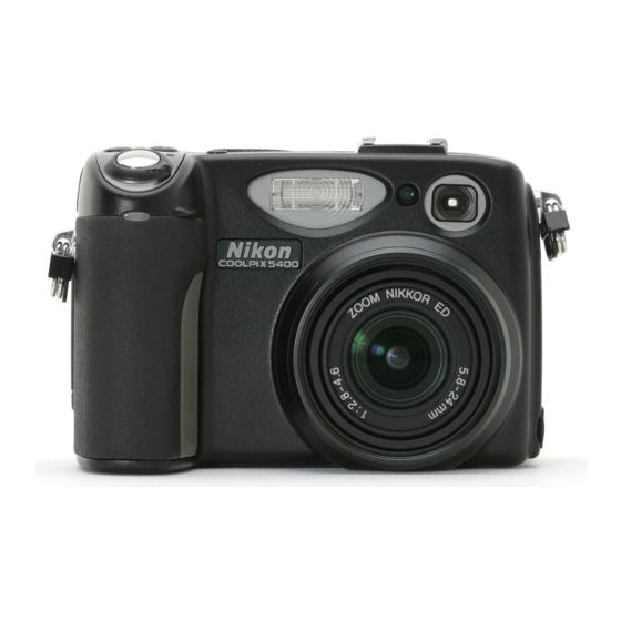
Nikon Coolpix 5400 Repair Manual
Hide thumbs
Also See for Coolpix 5400:
- Manual (173 pages) ,
- Instruction booklet (4 pages) ,
- How to upgrade firmware (10 pages)

Related Manuals for Nikon Coolpix 5400


Summary of Contents for Nikon Coolpix 5400
- Page 1 VAA14001-R.3603.A 配布許可印 作成承認印 VAA14001 REPAIR MANUAL NIKON CORPORATION Tokyo, Japan Copyright c 2003 by Nikon Corporation. All Rights Reserved. Recycled paper 無断転載を禁ず !! 再生紙を使用しています Printed in Japan July 2003...
-
Page 2: Table Of Contents
CONTENTS SPECIFICATIONS ····································································································································· M1-M2 DISASSEMBLY WARNING ·················································································································································D1 REAR COVER UNIT/FRONT COVER ···································································································D2 DISCHARGE OF MAIN CONDENSER ··································································································D3 LCD UNIT ·················································································································································D3 JOINT UNIT ··············································································································································D5 LENS HOLDER/BATTERY COVER/CF CARD COVER·······································································D6 CF CARD HOLDER··································································································································D6 BATTERY HOLDER/SPEED LIGHT UNIT/PW1 PCB···········································································D7 ① Separation from CP1 PCB·····················································································································D7 ②... - Page 3 DMA CIRCUIT DIAGRAM···················································································································· E13 VF1 CIRCUIT DIAGRAM······················································································································ E14 PW1 CIRCUIT DIAGRAM ····················································································································· E15 SYSTEM BLOCK DIAGRAM················································································································ E16 SYA CIRCUIT DIAGRAM······················································································································ E17 TB1 BLOCK DIAGRAM ························································································································ E18 TB2 BLOCK DIAGRAM ························································································································ E19 TB3 BLOCK DIAGRAM ························································································································ E20 TB4 BLOCK DIAGRAM ························································································································ E21 POWER BLOCK DIAGRAM ·················································································································...
-
Page 4: Specifications
SPECIFICATIONS Model Nikon Digital Camera E5400 Effective pixels 5.1 megapixels Image pixels 1/1.8 type primary-color CCD Total pixels: 5.26 megapixels Record pixels pixel 2592 × 1944 1280 × 960 2592 × 1728 3 2 1024 × 768 1600 × 1200 640 ×... - Page 5 AC adapter/battery charger EH-21 (sold separately) Continuous shooting time Approx. 110 minutes (when EN-EL1 is used and LC monitor lights at 20°C) * Measurement conditions are specifi ed by Nikon. (Zooming at each shooting, shooting with approx. 30% fl ash in NORMAL mode) External dimensions Approx.
-
Page 6: Disassembly
DISASSEMBLY WARNING There are high voltege parts inside. Be careful of this electric shock, when you remove the cover. You must discharge the main condenser according to the instruction of this repair manual before you remove the cover. Notes for the product in which the lead-free solder is used •... -
Page 7: Rear Cover Unit/Front Cover
REAR COVER UNIT/FRONT COVER Flash holder Connector DC jack cover CF card cover Connector USB cover USB holder Front cover • Open the CF card cover. • Disconnect the connectors • Open the DC jacket cover. • Remove the rear cover. •... -
Page 8: Discharge Of Main Condenser
DISCHARGE OF MAIN CONDENSER WARNING There are high voltege parts inside. Be careful of this electric shock, when you remove the cover. You must discharge the main condenser according to the instruction of this repair manual before you remove the cover. 2KΩ/5W Main condenser LCD UNIT... - Page 9 VAA14001-R.3603.A ② ① • Turn the LCD unit by 90° in the arrow mark direction. • Remove the 2 screws ① (M2×3). • Remove the 2 screws ② (large head). • Remove the LCD rear cover. LCD rear cover ⑥ FPC ①...
-
Page 10: Joint Unit
Soldering bridge VF1 PCB LCD side holder LCD holder Front LCD cover LCD unit Fig. 1 Spacer • Remove the LCD side holder ① . • The VF1 PCB and LCD unit can be removed. • When removing the LCD holder from the VF1 PCB, remove the 2 soldering bridges from the VF1 PCB. (Refer to Fig. -
Page 11: Lens Holder/Battery Cover/Cf Card Cover
LENS HOLDER/BATTERY COVER/CF CARD COVER CF card cover Shaft Connector Lens holder Shaft Battery cover Connector • Remove the 3 screws ① (M1.7×3). • Disconnect the connectors ② and ③ and then remove the lens holder. • Remove the 2 screws ④ (M1.7×2.5) and then remove the TB4 PCB ⑤ . •... -
Page 12: Battery Holder/Speed Light Unit/Pw1 Pcb
BATTERY HOLDER/SPEED LIGHT UNIT/PW1 PCB Separation from CP1 PCB • Remove the FPC ① . • Disconnect the connectors ② and ③ . • Float the microphone ④ from the PCB. (Refer to Fig. 1.) • Remove the screw ⑤ (M1.7×2.5). (Refer to Fig. 1.) •... -
Page 13: ② Aseparation Of The Battery Holder And Speed Light Unit From Pw1 Pcb
Separation of the battery holder and speed light unit from PW1 PCB Connector PW1 PCB Spacer Battery holder • Remove the 4 screws ① (M1.7×4). Speed light unit • Disconnect the connector ② . The speed light unit can be removed. •... -
Page 14: Finder Unit
FINDER UNIT Finder unit • Take off the FPC ① . • Remove the 3 screws ② (M1.4×3.5). • Remove the fi nder unit. - D9 E5400 -... -
Page 15: Assembly
ASSEMBLY FINDER UNIT Gear hole V groove cam Fig.1 Finder cam Finder cover • Turn the fi nder cam in the arrow mark direction of Fig. 1 until it contacts with the stopper. Approx. 2mm • Return the fi nder cam by half a turn. Where the distance is approx. -
Page 16: Ccd/Usb Holder, Lens/Finder Unit
CCD/USB HOLDER, LENS/FINDER UNIT • Set the spacer , mounting lens and CCD to the CP1 PCB. • Perform soldering on the CP1 PCB. • Attach the USB holder base and USB holder with the screw (M1.7 × 2.5). (Tighten the screw temporarily so that play can remain in the USB holder base •... -
Page 17: Battery Holder/Speed Light Unit/Pw1 Pcba3
BATTERY HOLDER/SPEED LIGHT UNIT/PW1 PCB Set the battery holder and speed light unit onto the PW1 PCB. • Attach the holder frame with the 2 screws (M1.7 × 2.5). Cord arrangement Connector PW1 PCB Spacer Battery holder Speed light unit Connector Cord arrangement •... -
Page 18: Setting To The Cp1 Pcb
VAA14001-R.3603.A ② Setting to the CP1 PCB • Connect the FPC ① to the PW1 PCB and CP1 PCB. (Refer to the figure for the direction of FPC ① .) Note: If you connect the FPC ① in the reversed direction, the power supply system will short-circuit. -
Page 19: Cf Card Holder
CF CARD HOLDER • Set the CF card holder by hitching 2 hooks. • Attach the 2 screws (M1.7 × 4). CF card holder Hook CF CARD HOLDER/BATTERY COVER/LENS HOLDER CF card cover Connector Lens holder Shaft Connector • As pushing the CF card cover against the camera main unit, slide it in the arrow mark direction and attach it. •... -
Page 20: Joint Unt
JOINT UNT • Set the TB1 PCB and attach the screw (M1.7 × 2.5). • Set the monitor cover. • Attach the screw (M1.7 × 2). • Attach the screw (M1.7 × 4). • Fit the lower harness side of the joint cover fi rst. (Arrow mark •... - Page 21 VAA14001-R.3603.A • Set the joint unit onto the front LCD cover. • Attach the screw ① (M1.7 × 3). • Connect the FPC ② . • Connect the FPC ③ . • Connect the connector ④ . • Connect the connector ⑤ . Note: Treat the codes according to Fig.
- Page 22 • Pass the connector through the hole of the rear cover and pull it to the inside of the rear cover. • Set the harness cover into the hole of the rear cover. (Refer to Fig. 1.) • Set the LCD unit onto the rear cover. •...
-
Page 23: Front Cover
VAA14001-R.3603.A FRONT COVER • Fit the notch of the lens spacer to the concave section of the lens barrel. Then, set the lens spacer onto the lens barrel. (Refer to Fig. 1.) • Set the front cover. (Set it so that the TB2 PCB connector can come out from the top of the FPC ① .) •... -
Page 24: Rear Cover
REAR COVER Connector Connector USB cover USB holder • Connect the FPC • Connect the FPC • Connect the connector • Connect the connector • Set the rear cover onto the camera main unit. (Be careful not to catch the cords and FPC.) •... -
Page 25: Pcb Arrangement
PCB ARRANGEMENT PW1 PCB CP1 PCB VF1 PCB TB3 PCB TB PCB TB2 PCB TB4 PCB - A11 E5400 -... -
Page 26: Adjustment
VAA14001-R.3603.A ADJUSTMENT 1. Equipment • Personal computer • AC adapter (EH-21) • USB cable ( UC-E1) • Oscilloscope 2. Servicing Tools • Pattern box • Color meter • Luminance meter • Siemens star chart • Calibration software 3. Adjustment Items and Order 1. - Page 27 VAA14001-R.3603.A - A13 ・ E5400 -...
- Page 28 VAA14001-R.3603.A 7. Adjustment items required at replacement of parts Lens Adj. CCD Defect LCD Panel Lens unit ○ ○ ○ × × Optical filter ○ ○ ○ × × ○ ○ ○ × × P-1 PCB ○ ○ ○ ○ △...
- Page 29 VAA14001-R.3603.A 9. Calibration software After starting the applicable calibration software, the following is displayed on the PC monitor. 10. Lens Adjustment [Preparation] • Siemens star chart • Turn on the power switch of camera. [Adjustment condition] • Siemens start chart of A3 size or larger (Make a copy of A4 size siemens start chart which is attached to the service manual in enlarged A3 size or larger.) •...
- Page 30 VAA14001-R.3603.A 11. AWB Adjustment [Preparation] • Pattern box (Color temperature: 3100 ± 20K, Luminance: 900 ± 20 cd/m [Adjustment condition] • Set the distance to 0cm between the pattern box and camera (front of camera). Note: Be careful to prevent the disturbing light from entering. [Adjustment method] •...
- Page 31 VAA14001-R.3603.A 12. CCD White Point Defect Detect Adjustment [Adjustment condition] • While the shutter in the lens is closed, the defect of CCD pixels is read, the correction data are made and rewriting is done by the following procedure. The defect of CCD pixels is corrected for the upper 512 pixels. [Adjustment method] •...
- Page 32 2. Double-click “DscCalDi130a”. 3. Click the Get button in the USB storage window and check the USB storage data. VID: NIKON PID: NIKON DSC E5400 Serial: Rev.: 1.00 4. Check the “Serial” in the above USB storage data. If the displayed value is different from the serial number printed on the base of camera, enter the number on the base of camera.
- Page 33 VAA14001-R.3603.A 15. LCD Panel Adjustment [VF1 PCB (Side B): Measurement/adjustment place] CL425 (VR) CL421 (COM) CL427 (VB) CL426 (VG) CL415 (HDD) 15-1 LCD H AFC Adjustment [Preparation] • Oscilloscope • Power switch: ON [Adjustment method] 1. Double-click “DscCalDi130a”. 2. Set “VCO” to ON. (Click the check box to enter the mark “...
- Page 34 VAA14001-R.3603.A 15-3. LCD Gain Adjustment [Adjustment method] 1. Adjust LCD “Gain” so that the amplitude of CL426 is 4.0V ± 0.1Vp-p. [Note] “15-2. LCD RGB Offset Adjustment” should always be carried out first. 15-4. RED Brightness Adjustment [Adjustment method] 1. Adjust LCD “R Bright” so that the amplitude of CL425 is (VG-0.1) ± 0.1Vp-p with respect to the amplitude of CL426, VG.
- Page 35 VAA14001-R.3603.A 15-5. LCD Blue Brightness Adjustment [Adjustment method] 1. Adjust LCD "B Bright" so that the amplitude of CL427 is (VG+0.15) ± 0.1Vp-p with respect to the amplitude of CL426, VG. [Note] "15-2. LCD RGB Offset Adjustment" and "15-3. LCD Gain Adjustment" should always be carried out first.
-
Page 36: Circuit Description
1. CIRCUIT DESCRIPTION Pin 1 1-1. OUTLINE OF CIRCUIT DESCRIPTION 1. Outline The CP1 PCB is mainly composed of the following ICs: IC903 (ICX452AQ) CCD imager IC904 (CXD34400EN) V driver IC905 (AD9849AKST) CDS, AGC, A/D converter, H driver Pin 11 2. -
Page 37: Lens Drive Block Diagram
3. IC905 (H driver) and IC904 (V driver) H driver (part of IC905) and V driver (IC904) are AD9848/AD9849 necessary to generate the clocks (vertical transfer clock, VREF 2~36 dB horizontal transfer clock and electronic shutter clock) 10 or 12 PxGA DOUT which drive CCD. -
Page 38: Lcd Block
6. Circuit Description 6-1. Digital clamp 6-8. JPEG encoder and decoder By subtracting the averaged value of the CCD optical Picture data are compressed and extended by JPEG black section from the subsequent data, the black level method. of the CCD output data are made uniform. The aver- aged value of the CCD optical black section should be 7. - Page 39 1-2. PW1 POWER SUPPLY CIRCUIT DESCRIP- TION 1-2. Speed light control voltage, analog system pow- 1. Outline er output The power supply circuit is mainly composed of the fol- 5.1V (VSB1), 15V (VSB2), 5.0V (A), 15.0V (A) and lowing blocks. -7.6V (A) are outputted.
- Page 40 1-3. SYA CIRCUIT DESCRIPTION 1. Confi guration and Function For the overall confi guration of SYA block, refer to the block diagram. The 8-bit microprocessor (IC301) is the center of the SYA block, which controls the camera system condition (mode). The 8-bit-microprocessor handles the following functions.
- Page 41 ASIC TEST ASIC control signal L : ASIC RESET ADVREF ON AD VREF ON/OFF signal L : ON BKUPCTL Backup battery charge control L: Charge CLKSEL0 ARM system clock ON/OFF H : ON CLKSEL1 System clock selection PLLSEL0 System clock selection PLLEN PLL oscillation ON/OFF H : ON...
- Page 42 3. Key Operation For the details of key operation, refer to the instruction manual. SCAN SCAN PW_ON FUNC MONITOR MENU QUICK AE-L TEST WIDE TELE ← → ↑ ↓ AUTO PLAY SCENE MOVIE SET UP QUAL DIN CONNECT AV JACK LCD 反転...
- Page 43 LENS COMPACT FLASH 1AV4J11VA120G CN301 SCAN IN OA SCAN OUT 0 SCAN IN 1A 1AV4J11SL060G SCAN IN 5A CN174 SCAN IN 4A LCD AN LCD AN SCAN IN 2A LCD AN AL 3.2V LCD CA PWR LED LCD CA SELF LED LCD CA 1AV4J10UC150G 1AV4J10UC150G...
- Page 44 A15V -7.6V(A) LENS O_LPF TO MAIN IC101 Q9002 47, 48, 1~5, 8~12 VOUT IC905 IC903 CDS, A/D C AD11 AD9849AKST ICX452HQ AD11 ADCK H DRIVE XPBLK CLPOB 3.0V IC909 CCDCK TK11130CS CCDSD CCDEN 3.4V Q9001 XSG3 XSG1A IC904 XSG1,XSG3A,XSG3B,XSG5A,XSG5B XSG2A 17,20 3,6,7,9,11 15,16,19,21,23,24...
- Page 45 XF901 L9001 NFM18PC105R0J3D C1-62700/SX782-JNK BK1608LL241-T VOLTAGE: VIEW MODE C9024 Q9001 C9023 2SD1819A 0.01;B C9025 C9026 0.01;B AVDD1 C9038 1000P;B V-DRIVE CLPOB AVSS1 IC904 CLPDM DVDD2 R9035 47;1/16J CXD3440EN-1 HBLK IC905 PBLK DVSS2 R9036 5.6;1/16J AD9849AKST C9010 MODEL QAD9849AKST-J R9034 5.6;1/16J -8.0 XSUB -7.0...
- Page 46 - E11 E5400 -...
- Page 47 LENS BLOCK CCD BLOCK IC953 FOCUS DRIVER V Driver CDS/AGC/AD 5M Pixel LENS IC904 IC951 IC905 IC903 LENS DRIVER CN301 MRST RELEASE UNIT ZTEST Flash PLLEN D(0:15) CN302 16Mbit BACK SW UNIT PLLSEL0 A(0:20) IC121 PLLSEL1 CN303 SDRAM MODE DIAL SD(0:31) CLKSEL0 IC301...
- Page 48 1AV4J10UC150G IC953 CN107 UPD168110 C9521 LCDCK 0.1;F MODE LCDSD RESETB LCDSEN C9522 DMA_MAIN LGND 33P;CH C9524 FIL2 1000P;B IC101 IC101 12V(L) COSC IC101 C9525 FIL1 C1026 3.3V(D) R9504 1000P;B C1030 C1044 PGND2 0.1;F 0.1;F 1608 0.1;F C9523 7.5K;1/16D OUT2B OUT1B 0.1;F ASIC-U C1046...
- Page 49 Z1-62700/SX782-JNK CN172 SI4F TO TB1 R1709 100K;1/16J CN171 CN173 R1738 TCOM 0.1;B C1718 LCDCK 2.2;1/16J PCTL 10;F C1717 LCDSD 3216 PCTLB LCDSEN P_VID R1717 C1719 12V(L) 100K;1/16J 0.1;B 3.3V(D) C1721 47;6.3-T C1712 0.01;B R1707 VDD2 SIG.C 10;1/16J ASIC-U C1709 FOADJ R1711 ASIC-V 0.68;F...
- Page 50 (Li-ion*2 EL1) (Lithum 2CR5) (4V-8.4V) P1-62700/SX782-JNK CN502 1AV4L26B3450G BATTERY L5003 VOLTAGE: VIEW MODE BATTERY + JW501 D5002 1AV4J10HD020N BATTERY - IL-S-2P-S2L2-EF(JAE) RB050L-40 JW502 1608 PR502 F47K2R0C3LTND 2.0A 32V DC JACK JK501 1608 1AV4J11B5180N +15V(VSB2) D5001 PR501 HEC3110-015010(HOSIDEN) L5001 RB050L-40 F47K2R5C3LTND Q5102 D5101 L5101...
- Page 51 CN104 Q3001 DC_IN ALW3.2V UNREG UNREG SY IC302 DCIN BATTERY BLON Q3002 BLON BACKUP P ON RESET P ON PAON P(A)ON LCD ON BAT OFF LCD ON XCIN TO PW1 BOARD BATTERY BACK UP X3002 32KHZ Z3001 XCOUT BACKUP CTL XOUT AVref X3001...
- Page 52 Q3001 R3014 SWD 3.2V DTC123EE SCAN IN 100K;1/16J SCAN OUT DCIN PW_ON FUNC Q3004 DTC144EE MONITOR MENU QUICK AE-L TEST Y1-62700/SX782-JNK WIDE TELE AUTO PLAY AV_JACK SCENE MOVIE SETUP QUAL PICTL OM/ORZJ11VA120GZ MRST R3020 1AV4J11VA120G DIN CONNECT AV JACK LCD FLIP LCD OPEN BAT_DET F.LED(R)
- Page 53 S6001 ESE22MH24XK JW601 LCD_FLIP TO PIN1 TO VF1 CN172 T1-62700/SX782-JNK TO PIN2 JW602 - E18 E5400 -...
- Page 54 S6501 S6501 S6501 S6501 SW1AB-260-10T28 SW1AB-260-10T28 SW1AB-260-10T28 SW1AB-260-10T28 T2-62700/SX782-JNK CN651 BATTERY DETECT SCAN OUT 5 SCAN IN 6F TO CP1(SYA)CN306 - E19 E5400 -...
- Page 55 T3-62700/SX782-JNK JW631 S6301 S6301 S6301 S6301 TO PIN1 SIZ-011NST SIZ-011NST SIZ-011NST SIZ-011NST TO CP1(SYA) CN307 TO PIN2 LCD OPEN JW632 - E20 E5400 -...
- Page 56 AV JACK T4-62700/SX782-JNK JK851 1608 1AV4J10EX040G L8501 BK1608LL241-T CN851 1608 L8503 BK1608LM751-T VIDEO OUT AUDIO OUT L8502 BK1608LL241-T AV JACK 1608 TO CP1(DMA)CN102 - E21 E5400 -...
- Page 57 +15V(VSB2) Q5102,Q5106 +15.0V(A) T5001,Q5101 Q5103,Q5105 OUT1 CONVERTER -7.6V(A) TRANS Q5104,Q5106 +5.0V(A) +5V(VSB1) VR511 PAON OUT2 L5131,Q5131 +1.8V(D) STEP DOWN IC501 CIRCUIT SWITCHING L5141,Q5141 CONTROLL OUT3 STEP DOWN +3.3V(D) FA7709R CIRCUIT 6 31 +12V(L) Q5152,Q5153 L5151,Q5151 OUT4 STEP UP ANODE CIRCUIT LCD_AN CURRENT DETECTOR...
- Page 58 The contents of inspection standards and tools for E5400 [1] Inspection standards················································································R1 to R6 [2] Tools·································································································· T1 to T2 Conditions to be set and prepared for inspections 1. Physical stance to measure : On the applicable product, its lens shall be set fl at and its monitor shall be set to vertically stand up. 2.
- Page 59 Inspection standards Item Criteria Applied tool(s) External view Clearance/Difference • Clearance around the battery cover when it is closed at the Vernier calipers in height bottom: 0.6mm or less • Clearance of general sections: 0.3mm or less Difference in height: 0.15mm or less External/internal view •...
- Page 60 Item Criteria Applied tool(s) Distance measurement • Focus must be accurate in the selected area. Visual check (Select an AF area and check it.) Compelling ∞ • The distant view mark and fl ash prohibition mark must be displayed on LCD. (Set to “Compelling ∞”...
- Page 61 Item Criteria Applied tool(s) Quality of image Resolution The resolution must be in compliance with the following values EIAJ chart in EIAJ chart evaluation. Photoshop • Horizontal center: 1250 lines Fisheye-converter Vertical center: 1250 lines (FC-E9) Horizontal periphery: 850 lines Vertical periphery: 850 lines Set the conditions as follows: FINE, Auto-white balance, P mode, sensitivity 50, gradation...
- Page 62 Item Criteria Applied tool(s) Finder Visual quality • Image Visual check There must not be noticeable trouble in blur, flare, distortion, contrast, ghost, halation, color tone, etc. • Shading You can check the whole angle of view in fi nder. Operation •...
- Page 63 Item Criteria Applied tool(s) LCD and others Monitor LCD View, etc. • No shading in the LCD display range • Inclination of image and monitor frame must be within 75°. Field of view • Through image: 96 ∼ 100% • Playback image:98 ∼ 100% Bright pixels or dim pixels Bright Zone...
- Page 64 Item Criteria Applied tool(s) E l e c t r i c a l characteristics Battery check voltage Level 1 (Half battery mark) • 4.8 ± 0.2V (Primary battery) 7.3 ± 0.2V (Secondary battery) (While lowering the power supply voltage, lightly press the shutter release button.
- Page 65 Tool List New tool Name Remarks Tool No. LV-1450DC E4300, E3500, J63080 Pattern Box LV-1450DC E3100, E2100,E5400 Common LV-1450DC LV-1450DC J63080A Spare Harogen Lamp (For LV-1450DC) Exclusive J63081 Color Meter Minolta Color meter Common BM-3000 J63068 Luminance Meter BM-3000 Common - T1 E5400 -...
- Page 66 New tool Name Remarks Tool No. Ver.1.30a (E995,E775,E885 J65042 Calibration Software (Ver.1.30a) E5000, E2500, E4500 E5700, E4300, E3500 E3100, E2100,E5400) Common(E995,E775,E885 E5000, E2500, E4500 E5700, E4300, E3500 E3100, E2100,E5400) Siemens chart Common Attached in Service Manual J61201 Finder positioning pin - T2 E5400 -...
- Page 67 VAA14001-R.3603.A - T3 ・ E5400 -...
Need help?
Do you have a question about the Coolpix 5400 and is the answer not in the manual?
Questions and answers