Table of Contents
Advertisement
Quick Links
CDX-F5000C/F5005X
SERVICE MANUAL
Ver. 1.1 2006. 05
• The tuner and CD sections have no adjustments.
AUDIO POWER SPECIFICATIONS (US, Canadian model)
POWER OUTPUT AND TOTAL HARMONIC DISTORTION
23.2 watts per channel minimum continuous average power into
4 ohms, 4 channels driven from 20 Hz to 20 kHz with no more
than 5% total harmonic distortion.
CD player section
Signal-to-noise ratio
120 dB
Frequency response
10 – 20,000 Hz
Wow and flutter
Below measurable limit
Tuner section
FM
Tuning range
87.5 – 108.0 MHz (F5000C)
87.5 – 107.9 MHz (F5005X)
Aerial terminal
External aerial connector
Intermediate frequency 10.7 MHz/450 kHz
Usable sensitivity
9 dBf
Selectivity
75 dB at 400 kHz
Signal-to-noise ratio
67 dB (stereo),
69 dB (mono)
Harmonic distortion at 1 kHz
0.5% (stereo),
0.3% (mono)
Separation
35 dB at 1 kHz
Frequency response
30 – 15,000 Hz
MW/LW (CDX-F5000C)
Tuning range
MW: 531 – 1,602 kHz
LW: 153 – 279 kHz
Aerial terminal
External aerial connector
Intermediate frequency 10.7 MHz/450 kHz
Sensitivity
MW: 30 µV
LW: 40 µV
AM (CDX-F5005X)
Tuning range
530 – 1,710 kHz
Aerial terminal
External aerial connector
Intermediate frequency 10.7 MHz/450 kHz
Sensitivity
AM: 30 µV
Sony Corporation
9-877-563-02
2006E04-1
eVehicle Division
© 2006. 05
Published by Sony Techno Create Corporation
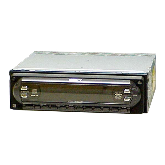
Photo: CDX-F5005X
Model Name Using Similar Mechanism
CD Drive Mechanism Type
Optical Pick-up Name
SPECIFICATIONS
Power amplifier section
Outputs
Speaker impedance
Maximum power output 50 W × 4 (at 4 ohms) (CDX-F5000C)
General
Outputs
Inputs
Tone controls
FM/MW/LW COMPACT DISC PLAYER
FM/AM COMPACT DISC PLAYER
US Model
Canadian Model
AEP Model
UK Model
NEW
MG-611XA-186//Q
KSS1000E
Speaker outputs
(sure seal connectors)
4 – 8 ohms
52 W × 4 (at 4 ohms) (CDX-F5005X)
Audio outputs terminal
(rear/sub switchable)
Power aerial relay control terminal (F5000C)
Power antenna relay control terminal (F5005X)
Power amplifier control terminal
Telephone ATT control terminal
Remote controller input terminal
BUS control input terminal
BUS audio input terminal
Antenna input terminal (F5005X)
Aerial input terminal (F5000C)
Low: ±10 dB at 60 Hz (XPLOD)
Mid: ±10 dB at 1 kHz (XPLOD)
High: ±10 dB at 10 kHz (XPLOD)
– Continued on next page –
CDX-F5005X
CDX-F5000C
CDX-F5000C
CDX-F5005X
1
Advertisement
Table of Contents

Related Manuals for Sony CDX-F5000C


Summary of Contents for Sony CDX-F5000C
- Page 1 (sure seal connectors) Wow and flutter Below measurable limit Speaker impedance 4 – 8 ohms Maximum power output 50 W × 4 (at 4 ohms) (CDX-F5000C) 52 W × 4 (at 4 ohms) (CDX-F5005X) Tuner section General Tuning range 87.5 – 108.0 MHz (F5000C) 87.5 –...
- Page 2 REPLACE THESE COMPONENTS WITH SONY PARTS WHOSE NE REMPLACER CES COMPOSANTS QUE PAR DES PIÈCES PART NUMBERS APPEAR AS SHOWN IN THIS MANUAL OR SONY DONT LES NUMÉROS SONT DONNÉS DANS CE MANUEL OU DANS LES SUPPLÉMENTS PUBLIÉS PAR SONY. IN SUPPLEMENTS PUBLISHED BY SONY.
- Page 3 CDX-F5000C/F5005X UNLEADED SOLDER Boards requiring use of unleaded solder are printed with the lead free mark (LF) indicating the solder contains no lead. (Caution: Some printed circuit boards may not come printed with the lead free mark due to their particular size.) : LEAD FREE MARK Unleaded solder has the following characteristics.
-
Page 4: Table Of Contents
CDX-F5000C/F5005X TABLE OF CONTENTS 1. GENERAL Location of controls ..............5 Connections ................6 2. DISASSEMBLY 2-1. Sub Panel Assy ..............8 2-2. CD Mechanism Block ............9 2-3. Main Board ................. 9 2-4. Chassis (T) Sub Assy ............10 2-5. -
Page 5: General
CDX-F5000C/F5005X SECTION 1 GENERAL This section is extracted from instruction manual. (CDX-F5000C) (CDX-F5005X) -
Page 6: Connections
CDX-F5000C/F5005X Connections (CDX-F5000C) - Page 7 CDX-F5000C/F5005X Connections (CDX-F5005X)
-
Page 8: Disassembly
CDX-F5000C/F5005X SECTION 2 DISASSEMBLY Note : This set can be disassemble according to the following sequence. 2-1. SUB PANEL ASSY (Page 8) 2-2. CD MECHANISM BLOCK (Page 9) 2-10. SERVO BOARD 2-3. MAIN BOARD 2-4. CHASSIS (T) SUB ASSY (Page 13) -
Page 9: Cd Mechanism Block
CDX-F5000C/F5005X 2-2. CD MECHANISM BLOCK 8 shield sheet 6 two screws (+PTT 2.6 x 4) 5 CD mechanism block 7 bracket (CD) 2 screw (+PTT 2.6 x 6) 1 screw (+PTT 2.6 x 6) 4 CNP301 2-3. MAIN BOARD 1 three ground point screws (+PTT 2.6 x 6) -
Page 10: Chassis (T) Sub Assy
CDX-F5000C/F5005X 2-4. CHASSIS (T) SUB ASSY 4 claw 2 two screws (+P 1.7 x 2.2) 1 two screws (+P 1.7 x 2.2) 6 chassis (T) sub assy 5 SENSOR board 3 claw 2-5. ROLLER ARM ASSY 3 washer 5 roller arm assy... -
Page 11: Chassis (Op) Assy
CDX-F5000C/F5005X 2-6. CHASSIS (OP) ASSY qa chassis (OP) assy 0 coil spring (damper) lever (D) 4 washer 1 CN2 9 two coil springs (damper) 5 gear (LE1) slider (R) 3 tension coil spring (KF) 2 Remove the six solderings. 2-7. OPTICAL PICK-UP... -
Page 12: Sl Motor Assy (M902)
CDX-F5000C/F5005X 2-8. SL MOTOR ASSY (M902) 1 screw (+P 1.4 x 1.8) 2 SL motor assy (M902) 2-9. LE MOTOR ASSY (M903) 8 screw 0 woam (LEB) assy (+M 1.7 x 2.5) 9 bearing (LEB) 2 washer qa screw (+M 1.7 x 2.5) -
Page 13: Servo Board
CDX-F5000C/F5005X 2-10. SERVO BOARD 6 SERVO board 1 Remove the eight solderings. 2 Remove the three solderings. 4 toothed lock screw (M 1.7) 5 claw 3 CN2... -
Page 14: Diagrams
CDX-F5000C/F5005X SECTION 3 DIAGRAMS 3-1. IC PIN DESCRIPTIONS • IC1 µPD63712GC-8EU-A (RF AMP, DIGITAL SERVO, DIGITAL SIGNAL PROCESSOR) (SERVO BOARD) Pin No. Pin Name Pin Description Laser diode ON/OFF control signal output (L: laser OFF, H: laser ON) Dimmer monitor input from optical pick-up laser diode. - Page 15 CDX-F5000C/F5005X Pin No. Pin Name Pin Description LRCK Not used. (Connect to LRCKIN in this set) DVDD — Power supply pin (+3.3 V) Focus servo drive PWM signal output (+) FD– Focus servo drive PWM signal output (–) Tracking servo drive PWM signal output (+) TD–...
- Page 16 XKEYON Key power supply control output Not used. (Open) KEYACK Key acknowledge detection input TU_ATTIN Mute zero cross detection input from tuner unit. (CDX-F5000C) 29, 30 Not used. (Open) BUIN Backup power supply detection input CD_INTQ CD text pack synchronization signal input from CD servo IC.
- Page 17 I2C_SIO I2C bus serial data input/output Not used. (Open) I2C_CKO I2C bus serial clock output DAVN RDS data block synchronization detection input (CDX-F5000C) SIRCS SIRCS signal input Not used. (Open) BEEP Beep output to power amp IC. 86 to 88 Not used.
- Page 18 Approx. 200mVp-p • Circled numbers refer to waveforms. • Signal path. (TEO) : FM : AM (CDX-F5000C) or MW (CDX-F5005X) : CD for printed wiring boards: — Main Board — • X : parts extracted from the component side. • Y : parts extracted from the conductor side.
-
Page 19: Block Diagram -Cd Section
CDX-F5000C/F5005X 3-2. BLOCK DIAGRAM — CD SECTION — RF AMP,DIGITAL SERVO, DIGITAL SIGNAL PROCESSOR OPTICAL PICK-UP (KSS1000E) (Page 20) TUNER SECTION LOUT ROUT DEMOD CONV SYSTEM CONTROL IC501 (1/3) INTQ CONV. 32 CD_INTQ CD_SO CD_SI FORCUS ERROR CD_SCK CD_STB CD_A0... -
Page 20: Block Diagram -Tuner Section
• Signal path BUSON 36 BUSIN TU-MUTE TU_ATT BUS ON SYSRST 37 : FM +5V REG. TU-VDD (TU5V) AUDIO 8.3V TH580 : AM (CDX-F5005X) or MW (CDX-F5000C) BATT VCC (8.3V) : CD • R-ch is omitted due to same as L-ch. -
Page 21: Block Diagram -Display Section
CDX-F5000C/F5005X 3-4. BLOCK DIAGRAM — DISPLAY SECTION — 3-5. CIRCUIT BOARDS LOCATION SYSTEM CONTROL LCD DRIVER IC501 (3/3) IC901 SERVO board KEY MATRIX SEG9 SENSOR board KEYIN0 LCDSO DATA S901-920 LCDCKO SEG66 KEYIN1 LCDCE S801 LCD901 COM1 COM4 D502 F5000C... -
Page 22: Printed Wiring Boards -Cd Mechanism Section
CDX-F5000C/F5005X 3-6. PRINTED WIRING BOARDS — CD MECHANISM SECTION — • Refer to page 18 for Common Note for Printed Wiring Boards. : Uses unleaded solder. JR90 JR41 (Page 24) M901 M902 M903... -
Page 23: Schematic Diagram -Cd Mechanism Section
CDX-F5000C/F5005X 3-7. SCHEMATIC DIAGRAM — CD MECHANISM SECTION — • Refer to page 18 for Common Note on Schematic Diagram and Waveforms. • Refer to page 30 for IC Block Diagrams. TP19 TP32 TP33 R14 R15 TP31 TP20 TP30 TP29... -
Page 24: Printed Wiring Board -Main Section
JW82 D720 Q471 JW128 CN702 D712 R505 R519 R671 R673 D751 Q478 R503 D502 D501 D719 D752 Q479 S501 D715 S702 D753 Q481 D754 Q580 G-11 D755 Q631 G-10 D756 Q651 D757 Q664 D758 Q701 ): CDX-F5000C only (Page 27) -
Page 25: Schematic Diagram -Main Section (1/2)
CDX-F5000C/F5005X 3-9. SCHEMATIC DIAGRAM — MAIN SECTION (1/2) — • Refer to page 18 for Common Note on Schematic Diagram and Waveforms. • Refer to page 30 for IC Block Diagrams. C765 C764 IC B/D C751 D751 IC51 C752 D752... -
Page 26: Schematic Diagram -Main Section (2/2)
CDX-F5000C/F5005X 3-10. SCHEMATIC DIAGRAM — MAIN SECTION (2/2) — • Refer to page 18 for Common Note on Schematic Diagram and Waveforms. (Page 25) (Page 23) IC602 IC681 C623 CNP301 C681 C683 C682 C622 S702 C301 C621 JC503 C343 L303... -
Page 27: Printed Wiring Board -Sub Section
CDX-F5000C/F5005X 3-11. PRINTED WIRING BOARD — SUB SECTION — • Refer to page 18 for Common Note on Printed Wiring Boards. : Uses unleaded solder. (Page 28) LED802 S801 CN801 D801 LED801 (Page 24) 3-12. SCHEMATIC DIAGRAM — SUB SECTION — • Refer to page 18 for Common Note on Schematic Diagram. -
Page 28: Printed Wiring Board -Key Section
G-10 LED902 LED913 C-13 LED922 D981 LED903 LED914 D-12 LED923 D983 LED904 LED915 D-11 LED961 B-11 LED905 LED916 D-10 LED962 IC901 LED906 LED917 D-10 IC971 LED907 LED918 (Q901) IC981 LED910 C-13 LED919 (Q902) LED911 B-12 LED920 Q961 ): CDX-F5000C only... -
Page 29: Schematic Diagram -Key Section
CDX-F5000C/F5005X 3-14. SCHEMATIC DIAGRAM — KEY SECTION — • Refer to page 18 for Common Note on Schematic Diagram. R981 R982 R983 R972 R996 IC971 LED922 LED919 LED916 LED913 LED912 LED923 LED907 LED961 R995 R927 R930 R933 R936 LED914 LED917... -
Page 30: Ic Block Diagrams
ANTI-ALIASING ANTI-ALIASING FILTER FILTER INPUT GAIN INPUT GAIN (0~15dB,1dB STEP) (0~15dB,1dB STEP) MUTE MUTE INPUT SELECTOR IC51 TDA7333-013TR (CDX-F5000C) (4 STEREO INCLUDE 1 ISOLATION INPUT) VCC/2 BAND PASS SINC4 SIGMA DELTA INTERPOLATOR FILTER FILTER CONVERTER VDDA INTN REF3... - Page 31 CDX-F5000C/F5005X IC750 TDA8588BJ/N2 OUT-FL- C BUS OUT-FL+ OUT-RL- PGND3 OUT-RL+ IN-RL IN-FL S-GND PROTECTION/ DIAGNOSTIC IN-FR IN-RR BEEP OUT-RR+ PGND2 OUT-RR- OUT-FR+ STANDBY/ MUTE OUT-FR- CHIP DETECT/ PGND1 DIAGNOSTIC BATTERY TEMPERATURE DIAG DETECTION ENABLE PROTECTION LOGIC SWITCH ANT-REM CRES AMP-REM SWITCH AUDIO8.3V...
-
Page 32: Exploded Views
CDX-F5000C/F5005X SECTION 4 EXPLODED VIEWS NOTE: • The mechanical parts with no reference • Color Indication of Appearance Parts The components identified by mark 0 or dotted line with mark number in the exploded views are not supplied. Example : 0 are critical for safety. -
Page 33: Front Panel Section
CDX-F5000C/F5005X 4-2. FRONT PANEL SECTION not supplied (KEY board) not supplied LCD901 not supplied not supplied not supplied not supplied supplied supplied not supplied Ref. No. Part No. Description Remark Ref. No. Part No. Description Remark A-3372-655-A PANEL COMPLETE ASSY, FRONT (F5005X) -
Page 34: Cd Mechanism Section (1)
CDX-F5000C/F5005X 4-3. CD MECHANISM SECTION (1) (MG-611XA-186//Q) not supplied (SENSOR board) not supplied not supplied Ref. No. Part No. Description Remark Ref. No. Part No. Description Remark A-3372-444-A CHASSIS (T) SUB ASSY 3-352-758-31 SCREW (M1.7), TOOTHED LOCK 3-253-729-11 SPRING (LTR), TENSION COIL... -
Page 35: Cd Mechanism Section (2)
CDX-F5000C/F5005X 4-4. CD MECHANISM SECTION (2) (MG-611XA-186//Q) (including M901) M902 not supplied not supplied not supplied not supplied not supplied The components identified by Les composants identifiés par une mark 0 or dotted line with mark marque 0 sont critiques pour 0 are critical for safety. -
Page 36: Cd Mechanism Section (3)
CDX-F5000C/F5005X 4-5. CD MECHANISM SECTION (3) (MG-611XA-186//Q) M903 Ref. No. Part No. Description Remark Ref. No. Part No. Description Remark 3-348-993-01 WASHER 3-259-467-11 BRACKET (LEM) 3-259-024-01 WHEEL (RA), WORM 3-345-648-91 SCREW (M1.4), TOOTHED LOCK A-3372-441-A ARM ASSY, ROLLER A-3372-450-A WORM (LEB) ASSY... -
Page 37: Cd Mechanism Section (4)
CDX-F5000C/F5005X 4-6. CD MECHANISM SECTION (4) (MG-611XA-186//Q) Ref. No. Part No. Description Remark Ref. No. Part No. Description Remark 3-259-429-11 WHEEL (LE), WORM 3-899-829-01 WASHER (SLIT) 3-344-223-01 WASHER 3-259-032-01 GEAR (LE2) 3-259-470-11 GEAR (LE1) A-3337-998-A CHASSIS (M) BLOCK ASSY 3-253-755-11 LEVER (D) -
Page 38: Electrical Parts List
CDX-F5000C/F5005X SECTION 5 ELECTRICAL PARTS LIST NOTE: • Due to standardization, replacements in • Items marked “*” are not stocked since The components identified by mark 0 or dotted line with mark the parts list may be different from the they are seldom required for routine service. - Page 39 CDX-F5000C/F5005X Ref. No. Part No. Description Remark Ref. No. Part No. Description Remark < RESISTOR > R945 1-216-809-11 METAL CHIP 1/10W R946 1-216-809-11 METAL CHIP 1/10W R901 1-216-819-11 METAL CHIP 1/10W R947 1-216-807-11 METAL CHIP 1/10W R902 1-216-819-11 METAL CHIP...
- Page 40 CDX-F5000C/F5005X MAIN Ref. No. Part No. Description Remark Ref. No. Part No. Description Remark R983 1-216-811-11 METAL CHIP 1/10W 1-126-947-11 ELECT 47uF R985 1-216-864-11 METAL CHIP 1/10W 1-126-947-11 ELECT 47uF R986 1-216-821-11 METAL CHIP 1/10W 1-162-970-11 CERAMIC CHIP 0.01uF R987...
- Page 41 CDX-F5000C/F5005X MAIN Ref. No. Part No. Description Remark Ref. No. Part No. Description Remark C462 1-125-891-11 CERAMIC CHIP 0.47uF CN702 1-784-456-11 CONNECTOR, FFC/FPC 14P C471 1-126-964-11 ELECT 10uF CNP301 1-817-536-11 CONNECTOR, BOARD TO BOARD 28P C479 1-126-947-11 ELECT 47uF C481...
- Page 42 CDX-F5000C/F5005X MAIN Ref. No. Part No. Description Remark Ref. No. Part No. Description Remark JC445 1-216-864-11 METAL CHIP 1/10W 1-414-595-11 INDUCTOR, FERRITE BEAD (F5000C) JC501 1-216-864-11 METAL CHIP 1/10W 1-414-595-11 INDUCTOR, FERRITE BEAD (F5000C) JC502 1-216-864-11 METAL CHIP 1/10W 1-216-801-11 METAL CHIP...
- Page 43 CDX-F5000C/F5005X MAIN SENSOR SERVO Ref. No. Part No. Description Remark Ref. No. Part No. Description Remark R508 1-216-864-11 METAL CHIP 1/10W R583 1-216-821-11 METAL CHIP 1/10W R509 1-216-813-11 METAL CHIP 1/10W R584 1-216-849-11 METAL CHIP 220K 1/10W R510 1-216-809-11 METAL CHIP...
- Page 44 CDX-F5000C/F5005X SERVO Ref. No. Part No. Description Remark Ref. No. Part No. Description Remark 1-107-826-11 CERAMIC CHIP 0.1uF 1-216-833-11 METAL CHIP 1/10W 1-107-826-11 CERAMIC CHIP 0.1uF 1-216-840-11 METAL CHIP 1/10W 1-107-826-11 CERAMIC CHIP 0.1uF 1-216-822-11 METAL CHIP 1.2K 1/10W 1-107-826-11 CERAMIC CHIP 0.1uF...
- Page 45 CDX-F5000C/F5005X Ref. No. Part No. Description Remark Ref. No. Part No. Description Remark < SWITCH > PARTS FOR INSTALLATION AND CONNECTIONS *************************************** S801 1-771-884-31 SWITCH, TACTILE (Z) X-3382-647-1 FRAME ASSY, FITTING ************************************************************* X-3382-926-1 SCREW ASSY (BS), FITTING (F5000C) MISCELLANEOUS 3-349-410-11 BUSHING (F5000C)
- Page 46 CDX-F5000C/F5005X REVISION HISTORY Clicking the version allows you to jump to the revised page. Also, clicking the version at the upper on the revised page allows you to jump to the next revised page. Ver. Date Description of Revision 2004. 01 2006.
Need help?
Do you have a question about the CDX-F5000C and is the answer not in the manual?
Questions and answers