Yamaha S03 Service Manual
Hide thumbs
Also See for S03:
- Owner's manual (112 pages) ,
- Data list (28 pages) ,
- Software installation manual (20 pages)
Table of Contents
Advertisement
This document is printed on chlorine free (ECF) paper with soy ink.
SY
011550
20010301-69800
MUSIC SYNTHESIZER
SERVICE MANUAL
CONTENTS
SPECIFICATIONS
BLOCK DIAGRAM
PANEL LAYOUT
CIRCUIT BOARD LAYOUT
WIRING
............................................................... 9
DISASSEMBLY PROCEDURE
LSI PIN DESCRIPTION
IC BLOCK DIAGRAM
CIRCUIT BOARDS
TEST PROGRAM
FACTORY SET
DISPLAY MESSAGES
MIDI IMPLEMENTATION CHART ......................................... 41
PARTS LIST
OVERALL CIRCUIT DAIGRAM
.............................................. 3/4
........................... 5
...................................... 6
................. 8
............................ 10
.............................. 15
................................... 17
......................................... 19
............................. 28/33
.................................. 39
............... 40
HAMAMATSU, JAPAN
1.494K-479 K
Printed in Japan '01.02
Advertisement
Table of Contents

Related Manuals for Yamaha S03


Summary of Contents for Yamaha S03
- Page 1 MUSIC SYNTHESIZER SERVICE MANUAL CONTENTS SPECIFICATIONS ..........3/4 BLOCK DIAGRAM ......5 PANEL LAYOUT ........6 CIRCUIT BOARD LAYOUT ....8 WIRING ............... 9 DISASSEMBLY PROCEDURE ......10 LSI PIN DESCRIPTION ......15 IC BLOCK DIAGRAM ........17 CIRCUIT BOARDS .........
- Page 2 IMPOR TANT NOTICE This manual has been provided for the use of authorized Yamaha Retailers and their service personnel. It has been assumed that basic service procedures inherent to the industry, and more specifically Yamaha Products, are already known and under- stood by the users, and have therefore not been restated.
-
Page 3: Specifications
PHONES (Stereo Phone), OUTPUT (Phone): L (MONO)/R, DC IN, FOOT CONTROLLER, FOOT SWITCH, TO HOST, MIDI IN/OUT/THRU DISPLAY LCD (Back Lit) POWER SUPPLY Yamaha AC adaptor PA-3B (included) POWER CONSUMPTION 7W (120V), 8W (230V) OUTPUT: +9 ±2dbm (10k ohms), PHONES: +0 ±2dbm (33 ohms) MAXIMUM OUTPUT LEVEL... - Page 5 IC013 IC016 TR1, 2, 3 (8P) (8P) JK002 MUTING OUTPUT Back BATTERY A/D L/MONO DO0, WCLK, QCLK UPD63200 JK003 IC018 (16P) OUTPUT SRAM SRAM FLASH (Lower) (Upper) Wave Wave IC013 IC016 Work Work Program JK001 (8P) (8P) IC006 IC007 IC004 IC003 IC005 (56P)
-
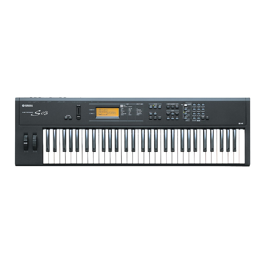
Page 6: Panel Layout
PANEL LAYOUT Front Panel o!0 ! 1 !4 OUTPUT STANDBY FOOT FOOT MIDI PHONES MONO DC IN CONTROLLER SWITCH TO HOST HOST SELECT THRU EDIT UTILITY MIDI MODE PART ELEMENT KEY CATEGORY DRUM SEARCH VOLUME MULTI PART MULTI VOICE DEMO MUTE VOICE COMMON... - Page 7 Rear Panel MIDI HOST SELECT FOOT FOOT STANDBY OUTPUT THRU TO HOST SWITCH CONTROLLER DC IN L MONO PHONES PC-2 MIDI q MIDI IN/OUT/THRU terminals w HOST SELECT switch e TO HOST terminal r FOOT SWITCH jack t FOOT CONTROLLER jack y STANDBY/ON switch u DC IN terminal i OUTPUT L/MONO and R jacks...
-
Page 8: Circuit Board Layout
CIRCUIT BOARD LAYOUT LCD Assembly Top Assembly Wheel Assembly Keyboard Assembly Keyboard Assembly Wheel Assembly MK-H MK-L MKS3... - Page 9 WIRING MK-L MK-H CN2(12P) CN3(7P) CN4(5P) MKS3 CN1(6P) CN1(15P) CN2(3P) CN1(6P) CN1(14P) Back Light Assembly CN5(5P) CN3(6P) CN4(15P) CN6(14P) Solder Wheel Board-in Assembly CN1(6P) Connector Adapter Screw Parts List Location Part No. Connector Assembly Destination Remarks Availability REF NO. Wheel (VU55440) WHEEL DM-CN5...
-
Page 10: Disassembly Procedure
DISASSEMBLY PROCEDURE Bottom Cover Assembly (Time required: About 10 min.) 1-1 Remove the thirty-four (34) screws marked [150]. The bottom cover assembly can then be removed. (Fig.1) Bottom Cover Assembly [150] [150] [150] [150] [150] [150] [150]: Bind Head Tapping Screw-B 4.0X8 MFZN2BL (EG340190) Fig.1 DM Circuit Board... - Page 11 Lithium Battery Battery VN103500 VN103600(Battery holder for VN103500) Notice for back-up battery removal Battery Push the battery as shown in figure, then the battery will pop up. Druk de batterij naar beneden zoals aangeven in de tekening de batterij Battery holder springt dan naar voren.
- Page 12 MKR angle [60A] [60A] [30A] [L60] [30A] [80] [60B] [100B] Keyboard Assembly MKF angle MKF angle MKF angle Wheel Assembly MKS3 [40] [40] [40] [30B] [40] [40] [30A]: Bind Head Tapping Screw-B 3.0X8 MFZN2BL (EP600190) [30B]: Bind Head Tapping Screw-P 3.0X8 MFZN2Y (EP600280) or [30B]: Bind Head Tapping Screw-P...
- Page 13 Wheel Assembly (Time required: About 10 minutes) 7-1 Remove the bottom cover assembly. (See procedure 1.) 7-2 Remove the four (4) screws marked [100B]. The wheel assembly can then be removed. (Fig.4) Keyboard Assembly (Time required: About 20 minutes) 8-1 Remove the bottom cover assembly. (See procedure 1.) 8-2 Remove the shield box assembly.
- Page 14 10. Assembling the keyboard assembly (Time required: About 30 minutes) 10-1 Install the white keys CEGB from the lower notes, and then install the DFA keys and C' key. Afterwards install the black keys from the higher notes, and tighten the twenty-one (21) screws marked [140].
-
Page 15: Lsi Pin Description
LSI PIN DESCRIPTION HG73C205AFD (XU947C00) SWX00B (Tone Generator) DM: IC001, 002 NAME FUNCTION NAME FUNCTION Initial clear CMA3 Program address bus RFCLKI PLL Clock CMA8 Program address bus PLL Control CMA2 Program address bus AVDD_PLL Power supply read signal AVSS_PLL Ground CMA1 Program address bus... - Page 16 HD63B05V0F073P (XR951A00) CPU MKS3: IC1 NAME FUNCTION NAME FUNCTION /RES Reset /INT Interrupt request Non-maskable interrupt Port C Port A ...
-
Page 17: Ic Block Diagram
MBCG46183-129 (XV833A00) SIO4 (Gate Array) DM: IC030 NAME FUNCTION NAME FUNCTION TX31 Transmit Data 31 Data Bus RX32 Receive Data 32 TX32 Transmit Data 32 /IRQ0 Interrupt Request Port 0 RX33 Receive Data 33 /IRQ1 Interrupt Request Port 1 TX33 Transmit Data 33... - Page 18 TC74VHC74FT (XV892A00) SN74HC138NSR (XW793A00) TC74VHC157F(EL) (XT475A00) Dual D-Type Flip-Flop 3 to 8 Demultiplexer 74VHC157SJX (XY870A00) SB: IC001 DM: IC028 Quad 2 to 1 Multiplexer DM: IC025 1CLR 2CLR SELECT Select STROBE Output Enable Output INPUTS OUTPUTS MM74HC245ASJX (XW107A00) SN74HC273N (IR027350) HD29051FP (XV708A00) SN74HC245N (IR024550) Octal D-Type Flir Flop...
-
Page 19: Table Of Contents
CIRCUIT BOARDS VOL Circuit Board (XZ146C0) ............19 DM Circuit Board (XZ144F0) ..........20,21/22,23 SB Circuit Board (X0143A0) ............20 LC Circuit Board (XZ147B0) ............22/23 SW Circuit Board (XZ145C0) ............24,25 MK-L Circuit Board (XR564C0) ............26 MKS3 Circuit Board (XU878B0) ............26 MK-H Circuit Board (XR565C0) ............27 Note: See parts list for details of circuit board component parts. -
Page 20: Dm Circuit Board (Xz144F0)
DM Circuit Board FOOT SWITCH MIDI HOST SELECT TO HOST THRU to SW-CN1 to Wheel Assembly to LC-CN1 SB Circuit Board SB Circuit Board Battery VN103500 to IC30-12pin VN103600(Battery holder for VN103500) to RA24-6pin Notice for back-up battery removal Battery Push the battery as shown in figure, then the battery will pop up. - Page 21 OUTPUT FOOT CONTROLLER STANDBY/ON DC IN L/MONO PHONES not installed to VOL-CN1 Component side to MKS3-CN1 2NA-V583600...
-
Page 22: Lc Circuit Board (Xz147B0)
DM Circuit Board LC Circuit Board to DM-CN4 Component side DM: 2NA-V583600 LC: 2NA-V626840... - Page 23 Pattern side LC Circuit Board Pattern side DM: 2NA-V583600 LC: 2NA-V626840...
-
Page 24: Sw Circuit Board (Xz145C0)
SW Circuit Board MODE PART/ELEMENT/KEY MULTI VOICE DEMO MUTE to VOL-CN2 to DM-CN6 UTILITY MIDI DEC/NO INC/YES DATA EDIT STORE LEFT DOWN RIGHT 2NA-V583530... - Page 25 CATEGORY SEARCH 7/PIANO 8/ORGAN 9/GUITAR (DRUM) MUTE 4/BASS 5/STRINGS 6/BRASS PRESET/DRUM/PERC INC/YES USER/SE 1/REED/PIPE 2/SYN LEAD 3/SYN PAD RIGHT GM/XG/OTHER 0/SYN COMP -/CHROMATIC PERCUSSION ENTER EXIT Component side Pattern side 2NA-V583530...
-
Page 26: Mk-L Circuit Board (Xr564C0)
MK-L Circuit Board to MK-H Component side MKS3 Circuit Board to MK-H to DM-CN3 Component side MK-L: 2NA-VV58380 MKS3: 2NA-V240490... -
Page 27: Mk-H Circuit Board (Xr565C0)
MK-H Circuit Board to MKS3-CN4 to MK-L Component side 2NA-VV583900... -
Page 28: Test Program
TEST PROGRAM (A) TEST PROGRAM LIST Press [INC/YES] to select and display the name of the next test in the test list. TEST No. TEST NAME Press [DEC/NO] to select and display the name of the preceding test RAM Battery in the test list. -
Page 29: Pitch Bend
Check that all panel switches operate correctly, and that LEDs switch If the key is operating normally, the unit will emit a sine-wave sound on and off accordingly. while you hold the key down, and the sound will stop when you release the key, If the check completes normally, the LCD displays OK and (Testing method) the test terminates. -
Page 30: Modulation Wheel
(Testing method) 06: PB Connect a foot controller to the [FOOT CONTROLLER] jack, and move the controller smoothly from lowest to highest (00 to 127) in yyy: next target value accordance with the LCD display. xxx: current data value 08: FC Check that the values change smoothly, with no snags. - Page 31 (Judgment result display) This test uses a test pattern (AA FF 00 55) to check MIDI IN/OUT/ THRU operation. 11: HST SEL (Testing method) Connect a MIDI cable to the [MIDI IN] and [MIDI OUT] connectors, and connect a MIDI monitor to the [MIDI THRU] connector. Then No change in display message start the test.
- Page 32 (Judgment result display) 13: OUT L Doing 20: RAM R/W (Check items) OUTPUT L: 880Hz +/- 3Hz, sine wave, +6.0 +/- 2dbm (10kohm load) (reference value: distortion not above 1.0%) 20: RAM R/W OUTPUT R: Not above -80dbm (10kohm load) PHONES (L): 880Hz +/- 3Hz, sine wave, -1.0 +/- 2dbm (33ohm load) (reference value: distortion not above 1.0%) * All original RAM data is preserved: the original data is saved out...
- Page 33 Press [ENTER] to restore the unit to its factory settings and terminate * On termination of test mode, the unit carries out its normal power- test mode. up sequence. * If you have restored factory settings (Factory Set operation, (Judgment result display) above), then after exiting test mode please confirm that the noise level (with all notes off) meets the following conditions.
- Page 39 FACTORY SET This lets you restore the synthesizer’s default Internal Voices (User Memory) and Multis, as well as its System and other settings. Once you edit any settings, the corresponding factory defaults will be overwritten and lost. Use the procedure below to restore the factory default settings.
-
Page 40: Display Messages
Host:off ...... HOST SELECT switch has been set to “off.” !BatteryLo ....The memory-backup battery is low; memory cannot be backed up. Store the necessary data to a MIDI data storage device such as Yamaha MIDI Data Filer MDF3, and have the battery changed. - Page 41 YAMAHA [ Music Synthesizer ] Date :27-DEC-2000 Model S03 MIDI Implementation Chart Version : 1.0 Function... Transmitted Recognized Remarks Basic Default 1 - 16 1 - 16 Memorized Channel Changed 1 - 16 1 - 16 Memorized Mode Default Messages...
-
Page 42: Midi Data Format
MIDI DATA FORMAT 1.2.7 Expression This message controls expression (dynamics within a musical line) for each part. It is used to create volume changes during a song. Channel messages Control# Parameter Data Range Expression 0...127 1.1 Note on/note off If the Multi Part parameter Rcv EXPRESSION = OFF, that part will not receive Expression. These messages convey keyboard performance data. - Page 43 1.2.16 Portamento Control NRPN Data Entry This message specifies the portamento source key number (the key number at which MSB LSB MSB LSB Parameter name and value range portamento will begin). Data of 0...127 specifies the portamento source key. 19H rr Drum instrument pitch fine When Portamento Control is received, the currently-sounding pitch will change at a rr : drum instrument note number...
-
Page 44: System Exclusive Messages
1.3 Channel mode messages 1.5 Pitch bend These messages specify the basic operation of a part. This message conveys movements of the pitch bender. This message is generally used to modify the pitch of a part, but the depth of the following 1.3.1 All Sound Off seven effects can be controlled. - Page 45 This message sets the MULTI EFFECT1 block (refer to tables <1-1>, <1-4>). 11110111 = End of Exclusive The S03 responds to this message only when it is set to the Multi mode. When this is received, the Volume MSB will be reflected by the System parameter 2.1.3.4 Multi Part parameter change MASTER VOLUME.
-
Page 46: Realtime Messages
This message requests transmission of a parameter value unique to the S03. Address and Byte Count are given in tables 1-n. Byte Count is indicated by the total size of The output is transmitted in the format of a S03 native parameter change (refer to 2.1.4). the Data in tables 1-n. -
Page 47: Midi Data Table
DRUM TOTAL SIZE 0F 31 0D 00 Drum Setup 2 The S03 responds to the message MODEL ID = 4C only when in the Multi mode. 00 - 7F CHORUS PARAMETER 11 Refer to Effect Type List 2E(depends on chorus type) - Page 48 0...127 n = DRUM SETUP NUMBER(0 - 1) TOTAL SIZE rr = NOTE NUMBER(0D - 5B) In the following cases, the S03 will initialize all Drum Setups. 00 - 01 Rcv PITCH BEND OFF, ON XG SYSTEM ON received 00 - 01 Rcv CH AFTER TOUCH(CAT)
- Page 49 00 - 7F REVERB PARAMETER 10 Multi Edit Buffer (nn=0) 00 - 7F REVERB RETURN - dB...0dB...+6dB(0...96...127) 40 Drum Voice S03 Kit (nn = 120 - 127) 01 - 7F REVERB PAN L63...C...R63 Bulk Footer Normal Voice PRESET (nn = 0 - 127)
- Page 50 00 - 7F CHORUS PARAMETER 5 “ 00( “ ) Address Size Data Parameter Description Default value 00 - 7F CHORUS PARAMETER 6 “ 1C( “ ) 00 - 7F CHORUS PARAMETER 7 “ 40( “ ) 00 - 5F AC1 CONTROLLER NUMBER 0...95 00 - 7F CHORUS PARAMETER 8 “...
- Page 51 Address Size Data Parameter Description Default value 00 - 0F Scaling Pan Table Number 0...65535, 1st bit3-0 bit15-12 00 00 - 0F 2nd bit3-0 bit11-8 00 - 0F 3rd bit3-0 bit7-4 00 - 01 Level Scaling Offset4 -128...+0...+127 00 - 0F 4th bit3-0 bit3-0 00 - 7F 00 - 0F Tuning Curve Table Number...
-
Page 52: Parts List
MUSIC SYNTHESIZER PARTS LIST CONTENTS OVERALL ASSEMBLY ..........2 TOP ASSEMBLY ..........4 KEYBOARD ASSEMBLY ........6 ELECTRICAL PARTS ..........8 Notes : DESTINATION ABBREVIATIONS A : Australian model M : South African model B : British model O : Chinese model C : Canadian model Q : South-east Asia model D : German model... - Page 53 OVERALL ASSEMBLY Top assembly: See page 4. Shield box assembly Keyboard assembly: See page 6. 140b Bottom cover assembly 140a 140b...
- Page 54 PART NO. DESCRIPTION REMARKS REF NO. RANK OVERALL ASSEMBLY (V654520) Top Assembly (V654650) V2386100 Keyboard Assembly 16M C61 MKS3 VU540700 Angle Bracket MK-FRONT EP600190 Bind Head Tapping Screw-B 3.0X8 MFZN2BL VU540900 Angle Bracket MK-REAR VJ999700 Bind Head Tapping Screw-B 3.0X20 MFZN2BL Shield Sheet (V762600) V6773400...
- Page 55 TOP ASSEMBLY Weel assembly VOL circuit board assembly SW circuit board assembly LCD assembly L120...
- Page 56 PART NO. DESCRIPTION REMARKS REF NO. RANK TOP ASSEMBLY (V654650) V6547600 Top Cover Shield Sheet (V763320) LCD Assembly (V654690) EP600190 Bind Head Tapping Screw-B 3.0X8 MFZN2BL Adhesive Tape 12X60 (VM72270) SW Circuit Board Assembly (V654710) EP600190 Bind Head Tapping Screw-B 3.0X8 MFZN2BL VOL Circuit Board Assembly (V654720)
- Page 57 KEYBOARD ASSEMBLY White key S8 S10 S9 S11 Circuit board assembly NOTE: Refer to the WIRING section of this manual regarding S4 , S5 , S6 , S7 connector assemblies.
- Page 58 PART NO. DESCRIPTION REMARKS REF NO. RANK V2386100 KEYBOARD ASSEMBLY 16M C61 MKS3 EP600280 Bind Head Tapping Screw-P 3.0X8 MFZN2Y EP630220 Bind Head Tapping Screw-P 3.0X8 MFZN2BL VU328600 Frame C61 16M VH1809C0 White Key CEGBDFA White Key CEGB (VH18090) White Key (VH18100) VH181100 White Key...
- Page 59 ELECTRICAL PARTS PART NO. DESCRIPTION REMARKS REF NO. RANK ELECTRICAL PARTS V5836000 Circuit Board (XZ144F0) Circuit Board (V759920)(X0143A0) V6760100 Circuit Board (XZ147B0) VV583900 Circuit Board MK-H (XR565C0) VV583800 Circuit Board MK-L (XR564C0) V2404900 Circuit Board MKS3 (XU878B0) V6760300 Circuit Board (XZ145C0) V6760200 Circuit Board...
- Page 60 PART NO. DESCRIPTION REMARKS REF NO. RANK US064100 C0092 Ceramic Capacitor-B (chip) 0.0100 50V K US064100 C0093 Ceramic Capacitor-B (chip) 0.0100 50V K UF037100 C0094 Electrolytic Cap. (chip) 10 16V UF037100 C0095 Electrolytic Cap. (chip) 10 16V US062680 C0096 Ceramic Capacitor-SL(chip) 680P 50V J UB052100 C0097...
- Page 61 PART NO. DESCRIPTION REMARKS REF NO. RANK VS201100 D0012 Diode D1F60 VT332900 D0013 Diode 1SS355 TE-17 VT332900 D0014 Diode 1SS355 TE-17 VV925900 D0015 Diode RLS-73 TE-11 VV617300 D0017 Diode RB751V-40 TE17 VV617300 D0018 Diode RB751V-40 TE17 VT332900 D0019 Diode 1SS355 TE-17 VT332900 -0022 Diode...
- Page 62 PART NO. DESCRIPTION REMARKS REF NO. RANK VR579900 L0041 Chip Inductance BK2125HS601-T VR579900 -0051 Chip Inductance BK2125HS601-T RD256470 R0001 Carbon Resistor (chip) 4.7K 0.1 J RD356100 R0002 Carbon Resistor (chip) 1.0K 63M J RD356100 R0003 Carbon Resistor (chip) 1.0K 63M J RD254560 R0004 Carbon Resistor (chip)
- Page 63 PART NO. DESCRIPTION REMARKS REF NO. RANK RD350000 R0089 Carbon Resistor (chip) 0 63M J RD359100 R0090 Carbon Resistor (chip) 1.0M 63M J RD357100 R0091 Carbon Resistor (chip) 10K 63M J RD357100 R0092 Carbon Resistor (chip) 10K 63M J RD350000 R0093 Carbon Resistor (chip) 0 63M J...
- Page 64 PART NO. DESCRIPTION REMARKS REF NO. RANK VR346900 TH001 Thermistor ERTD2FGJ801S 800 VV583800 Circuit Board MK-L (XR564C0) VV437800 Diode 1N4148(DO-34) VK025600 Wire Trap 52147 12P TE VK025100 Wire Trap 52147 7P TE VV583900 Circuit Board MK-H (XR565C0) VV437800 Diode 1N4148(DO-34) VK025600 Wire Trap 52147 12P TE...
- Page 65 PART NO. DESCRIPTION REMARKS REF NO. RANK VV439800 SW008 Tact Switch SKQNAJ STORE VV439800 SW009 Tact Switch SKQNAJ VV439800 SW010 Tact Switch SKQNAJ VV439800 SW011 Tact Switch SKQNAJ MUTE VV439800 SW012 Tact Switch SKQNAJ DEC/NO VV439800 SW013 Tact Switch SKQNAJ VV439800 SW014 Tact Switch...
- Page 66 S03 OVERALL CIRCUIT DIAGRAM 1/2 (DM, SB) to DM (K-5) to DM (G-7) DRAM 4M (DSP) to DM (I-4) to DM (K-5) to DM (K-4) to MKS3-CN1 to DM (K-5) to DM (K-7), to SB 1/2 (J-7) to DM (H-4)
- Page 67 S03 OVERALL CIRCUIT DIAGRAM 2/2 (LC, MKS3, MK-H, MK-L, SW, VOL) D1F60 (VS201100) NJM78L05UA(XJ598A00) D3FP3 (VZ016600) REGULATOR +5V DIODE MULTI VOICE DEMO EDIT PRESET USER GM/XG D-FF CATEGORY CATEGORY 1: OUTPUT SEARCH SEARCH 1: ANODE 2: COMMON 2: CATHODE 3: INPUT µPC2909T-E1(XT441A00)