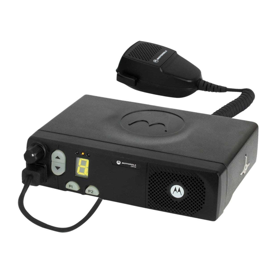
Motorola CM140 Service Information
Commercial series cm vhf1 (136-162mhz) low power
Hide thumbs
Also See for CM140:
- Basic user's manual (184 pages) ,
- User manual (5 pages) ,
- Service information (90 pages)

Related Manuals for Motorola CM140


Summary of Contents for Motorola CM140
- Page 1 Commercial Series CM Radios VHF1 (136-162MHz) Low Power Service Information Issue: October 2004...
-
Page 2: Computer Software Copyrights
Accordingly, any copyrighted Motorola computer programs contained in the Motorola products described in this manual may not be copied or reproduced in any manner without the express written permission of Motorola. Furthermore, the purchase of Motorola... -
Page 3: Table Of Contents
Table of Contents Chapter 1 MODEL CHART AND TECHNICAL SPECIFICATIONS 1.0 CM140/CM30/CM160/CM360 Model Chart ............1-1 2.0 Technical Specifications ..................1-2 Chapter 2 THEORY OF OPERATION 1.0 Introduction ......................2-1 2.0 VHF (136-162MHz) Receiver................2-1 2.1 Receiver Front-End ..................2-1 2.2 Receiver Back End ..................2-2 3.0 VHF Transmitter Power Amplifier (136-162 MHz) ..........2-2... - Page 4 8.3 Dual Tone Multiple Frequency (DTMF) Data ..........2-18 9.0 Receive Audio Circuits..................2-19 9.1 Squelch Detect ..................... 2-19 9.2 Audio Processing and Digital Volume Control..........2-20 9.3 Audio Amplification Speaker (+) Speaker (-) ..........2-20 9.4 Handset Audio....................2-21 9.5 Filtered Audio and Flat Audio ...............
-
Page 5: Model Chart And Technical Specifications
Chapter 1 MODEL CHART AND TECHNICAL SPECIFICATIONS Model Chart (VHF1 136-162 MHz) CM Series VHF1 136-162MHz Model Description MDM50JNC9AA2_N CM140 136-162 MHz 1-25W 8-Ch MDM50JNF9AA2_N CM160 136-162 MHz 1-25W 64-Ch MDM50JNF9AN2_N CM360 136-162 MHz 1-25W 100-Ch Item Description PMUD1936_ S. Tanapa VHF1 25W 8 Ch BNC PMUD1940_ S. -
Page 6: Technical Specifications
VHF1 Frequency Range: 136-162 MHz Frequency Stability ±2.5 PPM (-30°C to +60°C, 25°C Ref.) Channel Capacity: CM140 - 8 CM340 - 10 CM160 - 64 CM360 - 100 Channel Spacing: 12.5/20/25 kHz Power Supply: 13.8 Vdc (11 Vdc - 16.6 Vdc) negative Vehicle... - Page 7 Technical Specifications Transmitter Specification VHF1 Power Output 1-25W Conducted/Radiated -36 dBm < 1 GHz Emissions: -30 dBm > 1 GHz Audio Response: (from 6 dB/ oct. Pre-Emphasis, 300 to +1, -3dB 3000Hz) Tx Audio Distortion < 3% Modulation Limiting: ±2.5 kHz @ 12.5 kHz ±4.0 kHz @ 20 kHz ±5.0 kHz @ 25 kHz FM Hum and Noise:...
- Page 8 MODEL CHART AND TECHNICAL SPECIFICATIONS THIS PAGE INTENTIONALLY LEFT BLANK...
-
Page 9: Theory Of Operation
Chapter 2 THEORY OF OPERATION Introduction This Chapter provides a detailed theory of operation for the VHF circuits in the radio. Details of the theory of operation and trouble shooting for the associated Controller circuits are included in this Section of the manual. VHF (136-162MHz) Receiver Receiver Front-End The received signal is applied to the radio’s antenna input connector and routed through the... -
Page 10: Receiver Back End
THEORY OF OPERATION Receiver Back End The IF signal from the crystal filter enters the IF amplifier which provides 20 dB of gain and feeds the IF IC at pin 1. The first IF signal at 44.85 MHz mixes with the second local oscillator (LO) at 44.395 MHz to produce the second IF at 455 kHz. -
Page 11: Power Controlled Driver Stage
VHF Transmitter Power Amplifier (136-162 MHz) Op-amp U103-3 monitors the drain current of U101 via resistor R122 and adjusts the bias voltage of U101. In receive mode, the DC voltage from RX_EN line turns on Q101, which in turn switches off the biasing voltage to U101. -
Page 12: Harmonic Filter
THEORY OF OPERATION Harmonic Filter Inductors L111, L112 and L113 along with capacitors C1011, C1024, C1025, C1022, C1020, C1016 and C1017 form a low-pass filter to attenuate harmonic energy coming from the transmitter. Resistor R150 along with L126 drains any electrostatic charges that might otherwise build up on the antenna. -
Page 13: Fractional-N Synthesizer
VHF (136-162MHz) Frequency Synthesis This oscillator is temperature compensated to an accuracy of +/-2.5 PPM from -30 to 60 degrees C. The temperature compensation scheme is implemented by an algorithm that uses five crystal parameters (four characterize the inverse Bechmann voltage curve and one for frequency accuracy of the reference oscillator at 25 degrees C). -
Page 14: Voltage Controlled Oscillator (Vco)
THEORY OF OPERATION Voltage Controlled Oscillator (VCO) The Voltage Controlled Oscillator (VCO) consists of the VCO/Buffer IC (VCOBIC, U201), the TX and RX tank circuits, the external RX amplifier, and the modulation circuitry. AUX3 (U200 Pin 2) U200 Pin 32 Prescaler Out TRB IN Pin 20... -
Page 15: Synthesizer Operation
VHF (136-162MHz) Frequency Synthesis Synthesizer Operation The synthesizer consists of a low voltage FRAC-N IC (LVFRAC-N), reference oscillator, charge pump circuits, loop filter circuit, and DC supply. The output signal (PRESC_OUT) of the VCOBIC (U201, pin 12) is fed to the PREIN, pin 32 of U200 via a low pass filter which attenuates harmonics and provides a correct input level to the LVFRAC-N in order to close the synthesizer loop. -
Page 16: Controller Theory Of Operation
THEORY OF OPERATION Controller Theory of Operation This section provides a detailed theory of operation for the radio and its components. The main radio is a single-board design, consisting of the transmitter, receiver, and controller circuits. A control head is connected by an extension cable. The control head contains LED indicators, a microphone connector, buttons, and speaker. - Page 17 Controller Theory of Operation The DC voltage applied to connector P2 supplies power directly to the following circuitry: • Electronic on/off control • RF power amplifier • 12 volts P-cH FET -U514 • 9.3 volt regulator • Audio PA Ignition Control Head RF_PA Audio_PA...
-
Page 18: Protection Devices
2-10 THEORY OF OPERATION Voltage regulator U503 provides 5V for the RF circuits. Input and output capacitors are used to reduce the high frequency noise and provide proper operation during battery transients. VSTBY is used only for CM360 5-tone radios. The voltage VSTBY, which is derived directly from the supply voltage by components R5103 and VR502, is used to buffer the internal RAM. -
Page 19: Microprocessor Clock Synthesiser
Controller Theory of Operation 2-11 5.3.3 Emergency Mode The emergency switch (P1 pin 9), when engaged, grounds the base of Q506 via EMERGENCY _ACCES_CONN. This switches Q506 to off and consequently resistor R5020 pulls the collector of Q506 and the base of Q506 to levels above 2 volts. Transistor Q502 switches on and pulls U501 pin2 to ground level, thus turning ON the radio. -
Page 20: Serial Peripheral Interface (Spi)
2-12 THEORY OF OPERATION Serial Peripheral Interface (SPI) The µP communicates to many of the IC’s through its SPI port. This port consists of SPI TRANSMIT DATA (MOSI) (U403-pin100), SPI RECEIVE DATA (MISO) (U403-pin 99), SPI CLK (U0403-pin1) and chip select lines going to the various IC’s, connected on the SPI PORT (BUS). This BUS is a synchronous bus, in that the timing clock signal CLK is sent while SPI data (SPI TRANSMIT DATA or SPI RECEIVE DATA) is sent. -
Page 21: Normal Microprocessor Operation
Controller Theory of Operation 2-13 Normal Microprocessor Operation For this radio, the µP is configured to operate in one of two modes, expanded and bootstrap. In expanded mode the µP uses external memory devices to operate, whereas in bootstrap operation the µP uses only its internal memory. -
Page 22: Static Random Access Memory (Sram)
2-14 THEORY OF OPERATION Static Random Access Memory (SRAM) The SRAM (U402) contains temporary radio calculations or parameters that can change very frequently, and which are generated and stored by the software during its normal operation. The information is lost when the radio is turned off. The device allows an unlimited number of write cycles. -
Page 23: Transmit Audio Circuits
Transmit Audio Circuits 2-15 Transmit Audio Circuits 24kOhms TX SND TX RTN U509 CONTROL HEAD FILTERS AND CONNECTOR PREEMPHASIS ASFIC_CMP GCB3 U504 LIMITER HS SUMMER EXT MIC U509 SPLATTER FLAT TX FILTER AUDIO MOD IN ACCESSORY LS SUMMER CONNECTOR SECTION GCB5 (SYNTHESIZER) ATTENUATOR... -
Page 24: Ptt Sensing And Tx Audio Processing
2-16 THEORY OF OPERATION 7.1.2 Standard Microphone Hook Pin is shorted to the hook mic inside the standard Mic, If the mic is out off hook, 3.3V is routed to R429 via R458, D401, and it create 0.7V on MIC_SENSE (u.P U403-67) by Voltage Divider R429/R430. -
Page 25: Transmit Signalling Circuits
Transmit Signalling Circuits 2-17 Transmit Signalling Circuits SUMMER 5-3-2 STATE HIGH SPEED ENCODER CLOCK IN SPLATTER (HSIO) FILTER DTMF MICRO ENCODER CONTROLLER U403 ASFIC_CMP U504 LOW SPEED ENCODER SUMMER CLOCK IN (LSIO) TO RF ATTENUATOR SECTION MOD IN (SYNTHESIZER) Figure 2-8 Transmit Signalling Path From a hardware point of view, there are 3 types of signaling: •... -
Page 26: High Speed Data
2-18 THEORY OF OPERATION High Speed Data High speed data refers to the 3600 baud data waveforms, known as Inbound Signaling Words (ISWs) used in a trunking system for high speed communication between the central controller and the radio. To generate an ISW, the µP first programs the ASFIC CMP (U504) to the proper filter and gain settings. -
Page 27: Receive Audio Circuits
Receive Audio Circuits 2-19 Receive Audio Circuits ACCESSORY CONNECTOR FLT RX AUDIO AUDIO SPKR + EXTERNAL SPKR - U502 SPEAKER SPKR+ SPKR- CONTROL HEAD CONNECTOR MUTE U509 INTERNAL SPEAKER HANDSET AUDIO U505 GCB4 U IO AUDIO URX OUT GCB1 VOLUME AUX RX ASFIC_CMP ATTEN. -
Page 28: Audio Processing And Digital Volume Control
2-20 THEORY OF OPERATION Audio Processing and Digital Volume Control The receiver audio signal (DISC AUDIO) enters the controller section from the IF IC where it is.DC coupled to ASFIC CMP via the DISC input U504-pin 2. The signal is then applied to both the audio and the PL/DPL paths The audio path has a programmable amplifier, whose setting is based on the channel bandwidth being received, an LPF filter to remove any frequency components above 3000Hz, and a HPF to... -
Page 29: Handset Audio
Receive Signalling Circuits 2-21 Handset Audio Certain handheld accessories have a speaker within them which require a different voltage level than that provided by U502. For these devices HANDSET AUDIO is available at control head connector J2 pin18. The received audio from the output of the ASFIC CMP’s digital volume attenuator is routed to U505 pin 2 where it is amplified. -
Page 30: Alert Tone Circuits
2-22 THEORY OF OPERATION The low speed limited data output (PL, DPL, and trunking LS) appears at U504-pin18, where it connects to the µP U403-pin 80. The low speed data is read by the µP at twice the frequency of the sampling waveform; a latch configuration in the ASFIC CMP stores one bit every clock cycle. -
Page 31: Troubleshooting Charts
Chapter 3 TROUBLESHOOTING CHARTS This section contains detailed troubleshooting flowcharts. These charts should be used as a guide in determining the problem areas. They are not a substitute for knowledge of circuit operation and astute troubleshooting techniques. It is advisable to refer to the related detailed circuit descriptions in the theory of operation sections prior to troubleshooting a radio. -
Page 32: Troubleshooting Flow Chart For Receiver Rf (Sheet 1 Of 2)
TROUBLESHOOTING CHARTS Troubleshooting Flow Chart for Receiver RF (Sheet 1 of 2) START Problem No (Either 12.5K or 25K channel spacing having problem) in 12.5 KHz and 25 KHz channel spacing? 9V on Check Go to to U301 R310 (LNA) RX_EN DC Section Go to... -
Page 33: Troubleshooting Flow Chart For Receiver (Sheet 2 Of 2)
Troubleshooting Flow Chart for Receiver RF (Sheet 1 of 2) Troubleshooting Flow Chart for Receiver (Sheet 2 of 2) From Check visually all receiver Go to (IFIC -Vcc) components DC Section OK ? installation ? Inject - 40dBm (CW) Check to RF connector Installation the component... -
Page 34: Troubleshooting Flow Chart For 25W Transmitter (Sheet 1 Of 3)
TROUBLESHOOTING CHARTS Troubleshooting Flow Chart for 25W Transmitter (Sheet 1 of 3) START No or too low power when keyed Check components between >1.0A >430mA & <1.0A Q100 and RF output, Current Antenna Switch D104, increase when keyed? D103, VR102 and Q106 be- fore replacing Q100 <500mA Control... -
Page 35: Troubleshooting Flow Chart For 25W Transmitter (Sheet 2 Of 3)
Troubleshooting Flow Chart for 25W Transmitter (Sheet 1 of 3) Troubleshooting Flow Chart for 25W Transmitter (Sheet 2 of 3) Check PA Stages No or too low power when keyed Voltage Check U403 at Q101 & Q102 Check Q101, base=0? R153,R136, R165, R122, R168, R137 Check resistive network at... -
Page 36: Troubleshooting Flow Chart For 25W Transmitter (Sheet 3 Of 3)
TROUBLESHOOTING CHARTS Troubleshooting Flow Chart for 25W Transmitter (Sheet 3 of 3 Check Final PA Stage Supply Voltage PA_Bias <2V Replace Q100 Voltage at R134 2.1V 2-3V Check Bias Tuning R134, R131, R106 before replacing RF Voltage ASFIC U504 Check FGU after C1044 - >100mV? Check components... -
Page 37: Troubleshooting Flow Chart For Synthesizer
Troubleshooting Flow Chart for Synthesizer Troubleshooting Flow Chart for Synthesizer 5V at Check 5V U200 pins 5, Start Regulator 20, 34 & 36 U503 Visual Correct check of the Problem Board OK? Is 16.8MHz 16.8MHz Replace Signal at signal at U200 Is U200 U200 Pin 19? -
Page 38: Troubleshooting Flow Chart For Vco
TROUBLESHOOTING CHARTS Troubleshooting Flow Chart for VCO Low or no RF Signal Low or no RF Signal TX VCO RX VCO at input to PA at TP1 Visual check Visual check Correct of board of board Problem Make sure U508 is working correctly and runner 3.3 DC at U201 5V DC at U201... -
Page 39: Troubleshooting Flow Chart For Dc Supply (1 Of 2)
Troubleshooting Flow Chart for DC Supply (1 of 2) Troubleshooting Flow Chart for DC Supply (1 of 2) Since the failure of a critical voltage supply might cause the radio to automatically power down, supply voltages should first be probed with a multimeter. If all the board voltages are absent, then the voltage test point should be retested using a rising-edge-triggered oscilloscope. -
Page 40: Troubleshooting Flow Chart For Dc Supply (2 Of 2)
3-10 TROUBLESHOOTING CHARTS Troubleshooting Flow Chart for DC Supply (2 of 2) D3_3V Check VDC on C5007 Go to Digital Section Check Voltage on V=3.3V C5041 Replace U510 Go to Start 9v<V<9.8v... -
Page 41: Allocation Of Schematics And Circuit Boards
Chapter 4 VHF1 PCB/ SCHEMATICS/ PARTS LISTS Allocation of Schematics and Circuit Boards VHF1 and Controller Circuits The VHF circuits are contained on the printed circuit board (PCB) which also contains the Controller circuits. This Chapter shows the schematics for both the VHF circuits and the Controller circuits. The PCB component layouts and the Parts Lists in this Chapter show both the Controller and VHF circuit components. - Page 42 VHF1 PCB/ SCHEMATICS/ PARTS LISTS THIS PAGE INTENTIONALLY LEFT BLANK...
- Page 43 VHF1 1-25W PCB 8486672Z01 / Schematics VHF1 1-25W PCB 8486672Z01 / Schematics FILT_SW_B+ FILT_SW_B+ COMP_B+ INTEGRATOR INTEGRATOR DET_VRVS DET_VRVS DET-VFWD DET_VFWD TX_EN TX_EN RX_EN RX_EN PWR_SET PWR_SET PA_CURRENT PA_CURRENT PA_BIAS PA_BIAS TX_INJ TX_INJ 73D02968C63-0 SHEET 1 OF 8 VHF1 Interconnection between Main Board and Power Amplifier Compartment...
- Page 44 VHF1 1-25W PCB 8486672Z01 / Schematics 8486672Z01_REV O R101 C1007 C1064 C5100 C1065 C1097 L122 VR693 C1113 C1099 C1008 C1009 C1001 C1088 R150 R102 C1115 VR501 C1114 VR500 C1016 C1017 L126 R179 R5082 C1063 R5081 C5096 C1098 R5083 C1033 C1087 C1068 M102 R123...
- Page 45 VHF1 1-25W PCB 8486672Z01 / Schematics 8486672Z01_REV O R113 C5000 R169 R114 C1055 R111 C5086 C1109 R127 R115 C1061 R126 U102 L117 R112 VR692 C1110 C1002 C1035 R404 R175 R403 C5083 R147 D100 VR503 R405 M111 R421 L500 C1092 R5049 L100 C5055 C5060...
- Page 46 VHF1 1-25W PCB 8486672Z01 / Schematics D3_3V FILT_SW_B+ FILT_SW_B+ D3_3V TX_EN SPI_CLK SPI_MOSI SPI_MISO RX_EN LOC_DIST RSSI SYNTH_CS SYNTH_LOCK ASFIC_CS DIGITAL CH_ACT SQ_DET LSIO HSIO F1200 uP_CLK VS_AUDIO_SEL J3 - RESET D3_3V J3-12 J3-25 SERIAL CLOCK VOICE STORAGE AUDIO SELECT J3-13 J3-17 SERIAL DATA SEND...
- Page 47 VHF1 1-25W PCB 8486672Z01 / Schematics TX_EN RX_EN FILT_SW_B+ (SOURCE) (SOURCE) (SOURCE) (SOURCE) (SOURCE) FILT_SW_B+ D3_3V FILT_SW_B+ SPI_MOSI D3_3V COMP_B+ COMP_B+ SPI_CLK ASFIC_CS PA_BIAS PA_BIAS CH_ACT PWR_SET PWR_SET SQ_DET PA_CURRENT LSIO PA_CURRENT HSIO TX_INJ F1200 uP_CLK DET_VFWD FILT_SW_B+ VS_AUDIO_SEL RESET VS_MIC TX_AUDIO_SEND_OPT_BRD DET_VRVS...
- Page 48 VHF1 1-25W PCB 8486672Z01 / Schematics PA_FILT_B+ (SOURCE) L100 IF109 1019447 L119 1019447 COMP_B+ R186 IF110 R137 39.K C1115 C1099 C1100 C1116 220.p 220.p C1053 C1000 C1110 C1109 C1106 C1089 C1107 C1103 C1112 FLT_9V 220.p 220.p 220.p 220.p 470p 470p C1027 C1072 R168...
- Page 49 VHF1 1-25W PCB 8486672Z01 / Schematics IF100 PA_CURRENT R132 R114 LM2904 100.K 10.K U102 Final_cur_sense R111 R177 C1095 R113 100. 220.p 10.K C1055 FILT_SW_B+_PA R101 C1056 C1073 R110 R112 R115 100.K 10.K C1058 R116 L117 10.K 1019447 C1025 C1024 4.7p 4.7p Coupler R104...
- Page 50 4-10 VHF1 1-25W PCB 8486672Z01 / Schematics L217 390nH C2000 C2015 C2034 R225 C2026 2.2uF 0.1uF 150. C2055 R228 C2025 D200 100. C2024 C2016 C2004 0.1uF 2.2uF R226 150. L200 C2027 D201 390nH C2005 C2023 C2035 2.2uF R202 XTAL1 XTAL2 C2036 C2001 C2013...
- Page 51 VHF1 1-25W PCB 8486672Z01 / Schematics 4-11 V_SF R231 L201 680nH C2011 C2038 R235 C2040 C2042 C2041 C2009 C2008 C2007 0.1uF 0.1uF 100n 0.1uF L209 R220 L208 510. 100nH 100nH C2010 C2039 100n C2021 L202 680nH R216 R215 C2022 3.9K 4.7K C2060 IF200...
- Page 52 4-12 VHF1 1-25W PCB 8486672Z01 / Schematics FRONT-END SHIELD Q304 Q306 R300 R310 R333 10.K 15.K R346 430. L302 LOC_DIST C321 10.K 1.2u C324 C330 MIXER SHIELD R345 470.p 10.K R335 220. RX_EN Q300 D305 Q301 R327 L303 R339 C331 C329 2.4K 1.2u...
- Page 53 VHF1 1-25W PCB 8486672Z01 / Schematics 4-13 U301 R315 TC7W04F R306 12.K C313 20.K 100n FL301 FLTR 1 IN U301 TC7W04F BW_SEL D302 R305 R316 D301 20.K 12.K C312 1 IN 100n R314 R326 R324 FL302 12.K 3.3K FLTR 2.4K C316 0.1uF C317...
- Page 54 4-14 VHF1 1-25W PCB 8486672Z01 / Schematics IF501 IF503 COMP_B+ L120 1019447 C1098 C1114 C1113 C1097 C1088 9.3V 220.p SOURCE L500 220.p POWER SUPPLY SOURCE U501 FILT_B+ 9.3V IF502 57R01 LM2941T VOUT ON_OFF R5081 6.34K C5005 C5015 C5074 C1087 C1034 C1122 C1123 C1124...
- Page 55 VHF1 1-25W PCB 8486672Z01 / Schematics 4-15 POST_LIMITER_FLAT_TX_AUDIO_RETURN_OPT_BRD R5024 C5056 C5101 100.K 100.n C5090 C5089 R5068 R5046 82.p 82.p R5022 AUDIO 6.2K 24.K 100.K R5023 100.K U506 R5056 R5045 FLAT_TX_AUDIO_INPUT_ACCESS_CONN LM2904 33.K 10.K C5055 U506 LM2904 R5025 C5081 C5033 100.K 100n R5057 C5032...
- Page 56 4-16 VHF1 1-25W PCB 8486672Z01 / Schematics D400 D3_3V D3_3V R462 D3_3V SCI_CH C410 FILT_SW_B+ LSIO 100n R451 R450 R439 FILT_SW_B+ CH_ACT 10.K 10.K 10.K SQ_DET TP404 TP406 TP410 HSIO SPI_MISO TEST_POINT TEST_POINT TEST_POINT Q407 SPI_MOSI OPT_DATA_R_OPBD Q400 D3_3V SPI_CLK uP_CLK ASFIC_CS R425...
- Page 57 VHF1 1-25W PCB 8486672Z01 / Schematics 4-17 FILT_SW_B+ Q403 D3_3V PROG_OUT-ALARM_4 R460 R401 1.5K 2.7K R444 TP405 TEST_POINT 10.K Q401 D3_3V Q415 BOOT_EN_IN_CH D3_3V R431 10.K VR400 C490 6.80 R436 R457 R459 D3_3V 33.K 3.3K 47.K Q412 R445 ACCESS_PTT 10.K R458 Q414 3.3K...
- Page 58 4-18 VHF1 1-25W PCB 8486672Z01 / Schematics U100 LM2904 R141 22.K L101 IF701 C1046 DET_VFWD C1045 C1075 C1071 FILT_SW_B+ R117 IF702 INTEGRATOR R140 22.K R164 R144 22.K 10.K C1049 C1082 U100 C1048 LM2904 R146 IF700 DET_VRVS 22.K L102 D101 C1047 C1076 73D02968C63-0 SHEET 3 OF 8...
-
Page 59: 2.1 Vhf1 Pcb 8486672Z01 Parts List 1-25W
VHF1 1-25W PCB 8486672Z01 / Schematics 4-19 2.1 VHF1 PCB 8486672Z01 Parts List 1-25W Circuit Motorola Circuit Motorola Circuit Motorola Description Description Description Ref. Part No. Ref. Part No. Ref. Part No. C1031 2113743E07 CER CHIP CAP .022UF C1063 2113741F25... - Page 60 4-20 VHF1 1-25W PCB 8486672Z01 / Schematics Circuit Motorola Circuit Motorola Circuit Motorola Circuit Motorola Description Description Description Description Ref. Part No. Ref. Part No. Ref. Part No. Ref. Part No. C1128 2113740F59 CAP CHIP REEL CL1 +/-30 220 C2028...
- Page 61 VHF1 1-25W PCB 8486672Z01 / Schematics 4-21 Circuit Motorola Circuit Motorola Circuit Motorola Circuit Motorola Description Description Description Description Ref. Part No. Ref. Part No. Ref. Part No. Ref. Part No. C338 2113740F57 CAP CHIP REEL CL1 +/-30 180 C403 2113743K15 CER CHIP CAP .100UF...
- Page 62 4-22 VHF1 1-25W PCB 8486672Z01 / Schematics Circuit Motorola Circuit Motorola Circuit Motorola Circuit Motorola Description Description Description Description Ref. Part No. Ref. Part No. Ref. Part No. Ref. Part No. C5068 2113741F25 CAP CHIP CL2 X7R REEL 1000 C5101...
- Page 63 VHF1 1-25W PCB 8486672Z01 / Schematics 4-23 Circuit Motorola Circuit Motorola Circuit Motorola Circuit Motorola Description Description Description Description Ref. Part No. Ref. Part No. Ref. Part No. Ref. Part No. FL304 9180469V06 SMD455KHZ 6 ELEMENT CER L126 2462587X69 IND CHIP LO-PRO 1200 NH 5%...
- Page 64 4-24 VHF1 1-25W PCB 8486672Z01 / Schematics Circuit Motorola Circuit Motorola Circuit Motorola Circuit Motorola Description Description Description Description Ref. Part No. Ref. Part No. Ref. Part No. Ref. Part No. R105 0680194M18 RES 51 OHMS 5% 1W R139 0662057A87...
- Page 65 VHF1 1-25W PCB 8486672Z01 / Schematics 4-25 Circuit Motorola Circuit Motorola Circuit Motorola Circuit Motorola Description Description Description Description Ref. Part No. Ref. Part No. Ref. Part No. Ref. Part No. R314 0662057A75 CHIP RES 12K OHMS 5% R346 0662057A73...
- Page 66 4-26 VHF1 1-25W PCB 8486672Z01 / Schematics Circuit Motorola Circuit Motorola Circuit Motorola Circuit Motorola Description Description Description Description Ref. Part No. Ref. Part No. Ref. Part No. Ref. Part No. R5041 0662057A82 CHIP RES 24K OHMS 5% R5072 0662057A65...
- Page 67 VHF1 1-25W PCB 8486672Z01 / Schematics 4-27 Circuit Motorola Description Ref. Part No. VR503 4813830G09 DIODE 3.3V 5% ‘CK’ 500MW _4684 VR504 4813830G09 DIODE 3.3V 5% ‘CK’ 500MW _4684 VR692 4813830A75 DIODE DUAL COM ANODE VR693 4813830A77 DIODE DL ZENER TVS 33V 1.0A...
- Page 68 4-28 VHF1 1-25W PCB 8486672Z01 / Schematics THIS PAGE INTENTIONALLY LEFT BLANK...
Need help?
Do you have a question about the CM140 and is the answer not in the manual?
Questions and answers