Yamaha PW8 Service Manual
Hide thumbs
Also See for PW8:
- Owner's manual (10 pages) ,
- Owner's manual (10 pages) ,
- Owner's manual (11 pages)
Advertisement
Quick Links
Download this manual
See also:
Owner's Manual
PA
011911
200807 オープンプライス
POWER SUPPLY
SERVICE MANUAL
CONTENTS(目次)
SPECIFICATIONS(総合仕様) .................................................3
DIMENSIONAL DIAGRAM(寸法図) ........................................3
PANEL LAYOUT(パネルレイアウト) ......................................4
CIRCUIT BOARD LAYOUT(ユニットレイアウト) .................5
DISASSEMBLY PROCEDURE(分解手順) ..............................6
IC BLOCK DIAGRAM(IC ブロック図) ..................................10
CIRCUIT BOARDS(シート基板図) .......................................10
BLOCK DIAGRAM(ブロックダイアグラム)
CIRCUIT DIAGRAM(回路図)
Copyright (c) Yamaha Corporation. All rights reserved. PDF
PW8
HAMAMATSU, JAPAN
&
'08.07
Advertisement
Chapters

Related Manuals for Yamaha PW8


Summary of Contents for Yamaha PW8
-
Page 1: Table Of Contents
DIMENSIONAL DIAGRAM(寸法図) ........3 PANEL LAYOUT(パネルレイアウト) ........4 CIRCUIT BOARD LAYOUT(ユニットレイアウト) ....5 DISASSEMBLY PROCEDURE(分解手順) ......6 IC BLOCK DIAGRAM(IC ブロック図) ........10 CIRCUIT BOARDS(シート基板図) ........10 PARTS LIST BLOCK DIAGRAM(ブロックダイアグラム) CIRCUIT DIAGRAM(回路図) 011911 HAMAMATSU, JAPAN 200807 オープンプライス Copyright (c) Yamaha Corporation. All rights reserved. PDF ’08.07 &... - Page 2 IMPORTANT NOTICE This manual has been provided for the use of authorized Yamaha Retailers and their service personnel. It has been assumed that basic service procedures inherent to the industry, and more specifically Yamaha Products, are already known and understood by the users, and have therefore not been restated.
-
Page 3: Specifications(総合仕様
SPECIFICATIONS(総合仕様) General Specifications +15V Green LED: On (+15 V), Off (less than +10 V or more than +21 V) -15V Green LED: On (-15 V), Off (less than -21 V or more than -10 V) Secondary Voltage +12V Green LED: On (+12 V), Off (less than +7.6 V or more than +18 V) +48V Green LED: On (+48 V), Off (less than +32 V) (Phantom Voltage) -
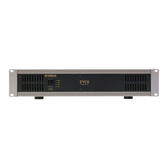
Page 4: Panel Layout(パネルレイアウト
PANEL LAYOUT(パネルレイアウト) Front Panel(フロントパネル) q POWER Switch q POWER スイッチ w Operation Monitor w オペレーションモニター (+48V, +12V, +15V, -15V) (+48V、+12V、+15V、-15V) Rear Panel(リアパネル) q DC PARALLEL INPUT Connector q DC PARALLEL INPUT 端子 w DC OUTPUT Connector w DC OUTPUT 端子 e AC IN Connector e AC IN 端子... -
Page 5: Circuit Board Layout(ユニットレイアウト
CIRCUIT BOARD LAYOUT(ユニットレイアウト) <TOP VIEW> DC ASSEMBLY (L) DC ASSEMBLY (R) (DC Ass’ y (L) ) (DC Ass’ y (R) ) <FRONT VIEW> FRONT PANEL 1(フロントパネル1)... -
Page 6: Disassembly Procedure(分解手順
DISASSEMBLY PROCEDURE(分解手順) The parts marked “※” are power transformer ※ HEXAGONAL NUT A components. (六角ナットA) TOP COVER (※は電源トランスの構成部品です。 ) (トップカバー) SHIELD BOARD (シールド板) [470] x 3 ※ PLATE A (プレートA) [470] x 3 ※ HEXAGONAL NUT B (六角ナットB) [300] x 6 ※... - Page 7 Top Cover トップカバー (所要時間:約 2 分) (Time required: About 2 minutes) Remove the eleven (11) screws marked [470]. The top [470] のネジ 11 本を外し、トップカバーを外しま cover can then be removed. (Fig. 1) す。 (図 1) Power Transformer 電源トランス (所要時間:約 3 分) トップカバーを外します。(1 項参照...
- Page 8 • DC ASSEMBLY (R) (DC ASS’ Y (R) ) • DC ASSEMBLY (R) (DC ASS’ Y (R) ) <LOWER VIEW> <TOP VIEW> INSULATION SHEET INSULATION SHEET (放熱シ−ト) (放熱シ−ト) DIODE STACK and TRANSISTOR DIODE STACK and TRANSISTOR (ダイオードスタックと トランジスタ) (ダイオードスタックと トランジスタ) Photo 4(写真4)...
- Page 9 AC1 Circuit Board AC1 シート (所要時間:約 3 分) (Time required: About 3 minutes) トップカバーを外します。(1 項参照 ) Remove the top cover. (See procedure 1.) [300] のネジ 6 本を外し、AC1 シートを外します。 Remove the six (6) screws marked [300]. The AC1 (図 1) circuit board can then be removed. (Fig. 1) PS Wiring Assembly PS 束線...
-
Page 10: Ic Block Diagram(Ic ブロック図
IC BLOCK DIAGRAM(IC ブロック図) μPC4570C (XC520A00) DC1: IC101 DC2: IC201, IC202 Dual Operational Amplifier +DC Voltage Output A Supply Inverting Output B Input A Non-Inverting Inverting Input A Input B Non-Inverting -DC Voltage Supply Input B CIRCUIT BOARDS(シート基板図) AC1 Circuit Board (X8678C0) ..............11 AC2 Circuit Board (X8678C0) ............. -
Page 11: Ac1 Circuit Board (X8678C0)
AC1 Circuit Board to AC3-CN301 to AC Inlet (AC WIRING ASSEMBLY) (ACインレット ( AC束線 ) ) to POWER TRANSFORMER (Primary) (電源トランス ( 一次側 ) ) to PS WIRING ASSEMBLY (OUTPUT) (PS束線 ( OUTPUT ) ) to DC1-CN103, DC2-CN203 to PS WIRING ASSEMBLY (PARALLEL INPUT) (PS束線... -
Page 12: Ac2 Circuit Board (X8678C0)
AC2 Circuit Board to DC2-CN202 Component side(部品側) AC3 Circuit Board to AC1-CN102 POWER ON/OFF Component side(部品側) AC2, AC3: 2NA-WJ98670... -
Page 13: Dc1 Circuit Board (X8679D0)
DC1 Circuit Board Scale: 80/100 to AC1-CN104 not installed not installed to DC2-CN204 to FAN (R) (DC ファン (R) ) to POWER TRANSFORMER (Secondary) (電源トランス ( 二次側 ) ) Component side(部品側) 2NA-WJ98680... -
Page 14: Dc2 Circuit Board (X8679D0)
DC2 Circuit Board Scale: 80/100 to AC2-CN201 to FAN (L) (DC ファン (L) ) to DC1-CN101 to POWER TRANSFORMER (Secondary) (電源トランス ( 二次側 ) ) not installed to AC1-CN104 2NA-WJ98680 Component side(部品側)... -
Page 15: Parts List
POWER SUPPLY PARTS LIST CONTENTS(目次) OVERALL ASSEMBLY(総組立) ........2 DC ASSEMBLY L(DC Ass’ y L) ........6 DC ASSEMBLY R(DC Ass’ y R) ........7 ELECTRICAL PARTS(電気部品) ......8–12 Notes : DESTINATION ABBREVIATIONS A : Australian model M : South African model B : British model O : Chinese model C : Canadian model... - Page 16 150a DC ASSEMBLY L (DC Ass’ y L) (See page. 6) DC ASSEMBLY R (DC Ass’ y R) (See page. 7) 150b...
- Page 17 150a 150b DC ASSEMBLY L(DC Ass’ y L) DC ASSEMBLY R(DC Ass’ y R) FRONT SIDE (See page. 6) (See page. 7)
- Page 18 150a DC ASSEMBLY L(DC Ass’ y L) 150b DC ASSEMBLY R(DC Ass’ y R) (See page. 6) (See page. 7) REAR SIDE REAR SIDE REAR SIDE...
- Page 19 PART NO. DESCRIPTION 部 品 名 REMARKS REF NO. RANK OVERALL ASSEMBLY 総 組 立 PW8 OVERALL ASSEMBLY 総 組 立 J (WM15230) OVERALL ASSEMBLY 総 組 立 U (WM15240) OVERALL ASSEMBLY H/K/C 総 組 立 H,B,O (WM15250) OVERALL ASSEMBLY 総...
- Page 20 PART NO. 部 品 名 REMARKS REF NO. QTY RANK DC ASSEMBLY L D C A s s ’ y L PW8 WM163500 DC ASSEMBLY L D C A s s ’ y L HEAT SINK (WM02310) ヒ ー ト...
- Page 21 PART NO. 部 品 名 REMARKS REF NO. QTY RANK DC ASSEMBLY R D C A s s ’ y R PW8 WM163600 DC ASSEMBLY R D C A s s ’ y R HEAT SINK (WM02310) ヒ ー ト...
- Page 22 ELECTRICAL PARTS (電気部品) AC1/AC2/AC3 and DC1/DC2 PART NO. DESCRIPTION 部 品 名 REMARKS REF NO. RANK ELECTRICAL PARTS 電 気 部 品 PW8 WM185300 CIRCUIT BOARD A C 1 シ ー ト J (WJ98670)(X8678C0) WM185600 CIRCUIT BOARD A C 1 シ...
- Page 23 DC1/DC2 PART NO. DESCRIPTION 部 品 名 REMARKS REF NO. RANK CIRCUIT BOARD DC2 J D C 2 シ ー ト (WJ98680,WM18630)(X8679D0) JUMPER WIRE 0.55 TIN ジ ャ ン パ ー 線 (VA07890) WC050700 FUSE HOLDER CLIP EYF52BCY ヒ ュ ー ズ ク リ ッ プ C101 WK624600 POLYESTER FILM CAPACITOR 0.3300 250V K ST...
- Page 24 DC1/DC2 PART NO. DESCRIPTION 部 品 名 REMARKS REF NO. RANK F102 V574250R FUSE TH 8.00A 250V ヒ ユ ー ズ 2 5 0 V F103 V574250R FUSE TH 8.00A 250V ヒ ユ ー ズ 2 5 0 V F201 KB000750 MINIATURE FUSE TL 2.00AT S ヒ...
- Page 25 DC1/DC2 PART NO. DESCRIPTION 部 品 名 REMARKS REF NO. RANK R201 HF75610R CARBON RESISTOR 1/4W 1.0K 1/4 J AX TP カ ー ボ ン 抵 抗 R202 HF75610R CARBON RESISTOR 1/4W 1.0K 1/4 J AX TP カ ー ボ ン...
- Page 26 PART NO. DESCRIPTION 部 品 名 REMARKS REF NO. RANK WA968500 FAN 2D85HJ200010 RDH80 D C フ ァ ン WIRING ASSEMBLY P S W 束 線 (WK72830) X8970A00 POWER TRANSFORMER ト ラ ン ス J X8971A00 POWER TRANSFORMER ト ラ ン...
-
Page 27: Parts List
POWER SUPPLY CIRCUIT DIAGRAM CONTENTS(目次) BLOCK DIAGRAM(ブロックダイアグラム) ....3 CIRCUIT DIAGRAM(回路図) AC1 ................4 AC2 ................4 AC3 ................4 DC1 ................5 DC2 ................6 Note: See parts list for details of circuit board component parts. 注: シートの部品詳細はパーツリストをご参照ください。 WARNING Components having special characteristics are marked and must be replaced with parts having specifi... - Page 28 BLOCK DIAGRAM (PW8) Main Q102N, Q103N Transformer Diode Bridge D108 F102 Heat sink TO-3P 2 Heat sink TO-220F Heat sink 250V +15V +25VDC D101 Regulator POWER C105 Voltage ON/OFF ZD105, 22000uF/35V ZD106 Detection F103 C106 Voltage 250V ZD107, ZD108 Detection...
- Page 29 AC1, AC2, AC3 CIRCUIT DIAGRAM (PW8) POWER ON/OFF to DC1-CN102 to DC2-CN201 not installed to DC2-CN202 (Secondary) (Primary) Toroidal Transformer only J not installed (Rear panel) to Transformer (Primary) installed (Gray) only AC Inlet U,H,B,O,A Yellow Brown H,B,O: Blue installed...
- Page 30 DC1 CIRCUIT DIAGRAM (PW8) not installed (Black) to Transformer (Red) (Secondary) (Red) to Fan (R) to DC2-CN204 OP AMP to AC1-CN104 OP AMP not installed : Mylar Capacitor(マイラーコンデンサー) 28CC1-2001033804-1 D25XB60 (VR14990R) FMU-22S (WD88620R) 2SC5395 (V2797700) 2SD1913 (VC407900) 2SB1274 (VC614000) ISA1993AS1 (WK608600) 2SA1386A/2SC3519A (V5611000) DIODE STACK 25.0A 600V...
- Page 31 DC2 CIRCUIT DIAGRAM (PW8) D25XB60 (VR14990R) DIODE STACK 25.0A 600V DC2: D201 to AC2-CN201 to Fan (L) FMU-22S (WD88620R) to DC1-CN101 DIODE STACK 10A 200V DC2: D209 not installed 2SC2240 (IC224030) TRANSISTOR DC2: Q210–214 (Orange) (Orange) OP AMP (Blue) (Blue)
-
Page 32: Parts List
POWER SUPPLY LINK CABLE PSL1010 PARTS LIST Notes : DESTINATION ABBREVIATIONS A : Australian model M : South African model B : British model O : Chinese model C : Canadian model Q : South-east Asia model D : German model T : Taiwan model E : European model U : U.S.A. -
Page 33: Parts List
PSL1010 PSL1010 PARTS LIST (パーツリスト) PART NO. DESCRIPTION 部 品 名 REMARKS REF NO. QTY RANK COMPLETE ASSEMBLY 同 梱 品 セ ッ ト PSL1010 COMPLETE ASSEMBLY 同 梱 品 セ ッ ト (WM95160) WM500100 POWER SUPPLY CABLE MH(S) 電 源...
Need help?
Do you have a question about the PW8 and is the answer not in the manual?
Questions and answers