Table of Contents
Advertisement
Quick Links
Download this manual
See also:
Instruction Manual
SERVICE MANUAL
7
2005
YD073
Since the whole mechanism assembly unit is replaced, the DVD recorder
1
PRECAUTION. . . . . . . . . . . . . . . . . . . . . . . . . . . . . . . . . . . . . . . . . . . . . . . . . . . . . . . . . . . . . . . . . . . . . . . . . 1-3
2
SPECIFIC SERVICE INSTRUCTIONS . . . . . . . . . . . . . . . . . . . . . . . . . . . . . . . . . . . . . . . . . . . . . . . . . . . . . . 1-6
3
DISASSEMBLY . . . . . . . . . . . . . . . . . . . . . . . . . . . . . . . . . . . . . . . . . . . . . . . . . . . . . . . . . . . . . . . . . . . . . . . 1-7
4
ADJUSTMENT . . . . . . . . . . . . . . . . . . . . . . . . . . . . . . . . . . . . . . . . . . . . . . . . . . . . . . . . . . . . . . . . . . . . . . . 1-11
5
TROUBLESHOOTING . . . . . . . . . . . . . . . . . . . . . . . . . . . . . . . . . . . . . . . . . . . . . . . . . . . . . . . . . . . . . . . . . 1-12
DVD VIDEO RECORDER
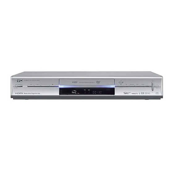
DR-M150SEK
S TA N D B Y / O N
TABLE OF CONTENTS
COPYRIGHT © 2005 Victor Company of Japan, Limited
RAM/RW
PR
PUSHÐOPEN
PR Ð
No.YD073
2005/7
Advertisement
Table of Contents

Related Manuals for JVC DR-M150SEK


Summary of Contents for JVC DR-M150SEK
-
Page 1: Table Of Contents
RAM/RW S TA N D B Y / O N PUSHÐOPEN PR Ð DR-M150SEK [D5R10] Since the whole mechanism assembly unit is replaced, the DVD recorder mechanism of this unit need not be adjusted. TABLE OF CONTENTS PRECAUTION............... . . 1-3 SPECIFIC SERVICE INSTRUCTIONS . - Page 2 SPECIFICATION DR-M150SEK GENERAL Power requirement AC 220 V - 240 V~, 50 Hz/60 Hz Power consumption Power on : 37 W Power off : 6.4 W Temperature Operating : 5°C to 35°C Storage : -20°C to 60°C Operating position Horizontal only Dimensions (W ×...
-
Page 3: Precaution
SECTION 1 PRECAUTION Safety Precautions (1) This design of this product contains special hardware and voltmeter. many circuits and components specially for safety purpos- Move the resistor connection to each exposed metal es. For continued protection, no changes should be made part, particularly any exposed metal part having a return to the original design unless authorized in writing by the path to the chassis, and measure the AC voltage across... - Page 4 Preventing static electricity Electrostatic discharge (ESD), which occurs when static electricity stored in the body, fabric, etc. is discharged, can destroy the laser diode in the traverse unit (optical pickup). Take care to prevent this when performing repairs. 1.5.1 Grounding to prevent damage by static electricity Static electricity in the work area can destroy the optical pickup (laser diode) in devices such as DVD players or recorder.
- Page 5 Important for laser products 5.CAUTION : If safety switches malfunction, the laser is able 1.CLASS 1 LASER PRODUCT to function. 2.DANGER : Invisible laser radiation when open and inter 6.CAUTION : Use of controls, adjustments or performance of lock failed or defeated. Avoid direct exposure to beam. procedures other than those specified here in may result in 3.CAUTION : There are no serviceable parts inside the hazardous radiation exposure.
-
Page 6: Specific Service Instructions
SECTION 2 SPECIFIC SERVICE INSTRUCTIONS This service manual does not describe SPECIFIC SERVICE INSTRUCTIONS. 1-6 (No.YD073) -
Page 7: Disassembly
SECTION 3 DISASSEMBLY Main body section 3.1.1 Remove the top cover (See figure 1) (1) Remove the four screws A attaching the top cover on both sides of the main body. (2) Remove the five screws B attaching the top cover on the TOP COVER TOP COVER TOP COVER... - Page 8 3.1.3 Remove the drive unit (See figure 4) Drive unit Digital board • Prior to performing the following procedure, remove the top cover. • There is no need to remove the front panel assembly. (1) Disconnect the socket wire from connector CN5301 on the main board.
- Page 9 3.1.5 Remove the main board (See figure 6, figure 7) • Prior to performing the following procedure, remove the top CN4001 CN1101 Display board cover, drive unit. CN5001 CN7001 Digital board (1) Disconnect the card wire from connectors CN4001, CN4103, CN6801, CN6802 on the main board.
- Page 10 3.1.7 Remove the digital tuner unit (See figure 9,figure 10) • Prior to performing the following procedure, remove the top Digital board CN6801 CN1404 cover. (1) Disconnect the card wire from connectors CN6801, CN6802, CN1404 on the main board and digital board. (2) Remove the two screws I attaching the digital tuner unit.
-
Page 11: Adjustment
SECTION 4 ADJUSTMENT This service manual does not describe ADJUSTMENT. (No.YD073)1-11... -
Page 12: Troubleshooting
SECTION 5 TROUBLESHOOTING JIG Mode The following remote control units are required to set and cancel JIG mode. For setting : a remote control unit attached to product. For cancellation : JIG remote control unit (part number : PTU94023B) Remote control unit JIG remote control unit attached to product JIG remote control unit... - Page 13 5.1.1 Setting JIG mode To display SYSTEM INFO or to upgrade firmware, the main body needs to be set to JIG mode. (1) Turn the main body ON. (2) Press the buttons of the remote control unit attached to product in the following order : "SET UP" → "2" → "8" → "ENTER" (3) When a colon ":"...
- Page 14 Displaying SYSTEM INFO In the SYSTEM INFO there is information including firmware versions of the main body and the drive unit. (1) Set the main body to JIG mode. (2) Transmit "43-8B" to the main body by using JIG remote control unit. (Please end a setting menu pushing “SET UP”...
- Page 15 Updating the firmware of the main body or digital video broadcasting tuner • Firmware update disk supports CD-R media. • When firmware update is necessary. information is available from the homepage of DIGITAL VIDEO STORAGE CATEGORY, CS group. • Please check the details of the update disc creation method by JS-NET. (1) Set the main body to JIG mode.
- Page 16 Taking out a disc 5.6.1 Method 1 There is compulsive tray ejection mode by electric operation. (1) AC Plug is pulled out at once and inserted again. (2) It is displayed on FL display as "PLEASE" and "WAIT" blink alternately, and while it blinks, pushing the EJECT button of a main body is continued.
- Page 17 Initialization to the factory shipment state When the initialization is operated, internal information changes as follows. It is essential to obtain the client’s permission before the operation. • All DVD library is all deleted. • All the DVD initial settings go back to the initial status. (1) Set to the JIG mode.
- Page 18 Victor Company of Japan, Limited AV & MULTIMEDIA COMPANY DIGITAL VIDEO STORAGE CATEGORY 12, 3-chome, Moriya-cho, kanagawa-ku, Yokohama, kanagawa-prefecture, 221-8528, Japan (No.YD073) Printed in Japan...
-
Page 19: Mechanism Of This Unit Need Not Be Adjusted
Project (1991 to 1996) Number : 3546 RAM/RW S TA N D B Y / O N PUSHÐOPEN PR Ð DR-M150SEK [D5R10] Since the whole mechanism assembly unit is replaced, the DVD recorder mechanism of this unit need not be adjusted. No.YD073SCH COPYRIGHT... - Page 20 CIRCUIT BOARD NOTES CHARTS AND DIAGRAMS 1. Foil and Component sides NOTES OF SCHEMATIC DIAGRAM 4. Voltage measurement 1) Foil side (B side) : Parts on the foil side seen from foil face (pattern face) 1) Regulator (DC/DC CONV) circuits Safety precautions are indicated.
-
Page 21: Wiring Diagram
Wiring diagram CN4401 CN7002 CN1102 CN1101 CN5302 p10745001a_rev1... -
Page 22: Block Diagrams
Block diagrams J7304 MAIN 0 3 L-1 SCART Terminal AUDIO OUT J7301 J8501 Audio signal control section (SHEET 2) IC8501 RAPID_SW BIAS/RGB_CTL COAXIAL OUT Q7310 to Q7312 AO_IEC958 4_3[L] P50_I/O AV_YC_IN[H] TV[L] A_MUTE2[H] TO SHEET 7 Muting AUDIO_OUT1[L/R] Q8203,Q8205 SWITCH AV1_L TO SHEET 4 IC7302... - Page 23 DIGITAL 5 0 J4112 IEEE1394 TPA+ TPA- TPB+ TPB- IEEE1394 controller terminal PHY_RESET[L] IC1801 PHY_LREQ PHY_CLK VI_D2 to D9 VIDEO_27M E5_RESET_L SIO_SCL SIO_SDA PHY_CNA PHY_CTL[0],[1] Video PHY_DATA[0-7] PHY_LPS decoder PHY_LINK_ON IC1901 C_IN VY_IN IEEE1394 section (SHEET 10) Video decoder section (SHEET 13) SDRAM_DQ16 to 31 DDR_DQ16 to 31 RA1613 to...
- Page 24 MAIN 0 3 RGB_YC 6 8 RGB-Y/C Converter section (SHEET 8) R_IN -29V DC3.9V[+/-] G_IN TO SHEET 9 AC-DC B_IN RGB-Y/C Converter Video AMP. AC IN IC4403 YOUT D5001 IC4401 IC4404 SW-12V SW12V SW5V AL5.8V D1.8V D2.5V TO each sheet H_OUT C_FROM_RGB REAR2_RC_IN...
- Page 25 Standard schematic diagrams Power supply section DC3.9V[+] Q5301 D5201 CP5301 R5319 TO SHEET 9 DC3.9V[-] -29V C5201 SW-12V FAN_CTL TO SHEET 5 P.CTL[H] D5202 R5307 DANGEROUS VOLTAGE SW12V Q5304 C5202 D5302 D5303 R5320 R5321 SW5V F5001 T5001 AL5.8V CN5001 C5102 LF5001 To each R5322...
- Page 26 Audio signal control section AV1_L AV2_H I2C_CLK2 I2C_DATA2 R8220 A_MUTE1[H] ADC_RST[L] Q8202 R8218 C8208 R8222 SHEET 5 R8223 Q8201 C8206 R8221 C8210 R8217 C8207 C8209 R8250 C8217 C8005 R8252 R8017 TU_AUDIO[R] R8040 R8219 R8249 TU_AUDIO[L] C8007 R8019 Q8205 SHEET 6 R8214 C8205 C8008...
- Page 27 Video signal control section L4301 C4318 C4319 R4319 C4310 IC4301 R4311 C4306 SW5V R4304 R4306 R4307 SHEET 1 R4314 C4302 C4301 C4308 C4307 R4313 I2C_DATA2 Q4302 Q4303 I2C_CLK2 R4317 R4318 C4304 C4305 D4301 C4309 SEPA_IN[H] PD[L] R4309 SHEET 5 R4305 R4308 IC4304 L4005...
- Page 28 Input/output terminal section J7309 4_3[L] TO SHEET 5 TV[L] R7302 R7339 R7340 Q7310 Q7302 P50_I/O R7378 Q7312 R7341 SCR_ID R7301 R7305 Q7301 R[H] Q7311 TO SHEET 5 R7309 BIAS/RGB_CTL R7304 R7342 AV1_YC_IN[H] D7304 RAPID_SW R7335 L7305 R7336 L7306 R7303 C7334 C7335 REAR1_C_IN R7343 C7332...
- Page 29 System controller section B7451 L7201 R7451 G_TX R7456 Q7201 IRTX R7452 SHEET 7 G_RX R7454 RGB_IN[H] SCR_ID CN7451 C7453 Q7451 SEPA_IN[H] SHEET 3 C7451 SECAM_DET[H] Not use Q7452 4_3[L] TV[L] R7203 R7453 RGB_TH[H] AV1_YC_IN[H] J7451 BIAS/RGB_CTL R7204 AV1_L SHEET 4 AV2_H P_MUTE[H] RAPID_SW...
- Page 30 Tuner section RF5V SW5V SW12V SHEET 1 SW3.3V SW2.5V C6803 CN6801 C6801 C6807 DVB Tuner C6805 C6802 unit L6002 C6804 C6806 C6808 TU6001 C6014 L6003 TU_AUDIO[L] SHEET 2 TU_AUDIO[R] C6013 C6012 C6831 C6832 CN6701 Not use L6701 R6080 C6751 C6752 C6027 C6028 L6005...
- Page 31 TO CN1103 SHEET 16 Input/output relay section TO CN1102 SHEET 16 TO CN1101 SHEET 16 CN4103 CN4102 CN4101 D1.8V D2.5V 3.3V TO SHEET 1 YTODIGI TO SHEET 3 CTODIGI PB/B_OUT PY/G_OUT SW5V PR/R_OUT AL5.8V TO SHEET 4 V/Y_OUT SC_OUT SY_OUT K_BUS_CLK K_BUS_REQ K_BUS_IN...
- Page 32 RGB-Y/C Converter section R4401 C4408 C4419 C4418 C4409 C4410 R4418 R4419 R4420 C4401 R4402 R4404 C4420 C4421 R4403 R4405 IC4402 C4413 C4412 R4414 C4411 CN4402 TO CN4401 SHEET 3 p30139001a_rev0 SHEET 8 2-25 2-26...
- Page 33 FL Display and operation switch section CN4104 B4*21 Q7101 D7106 K4*05 KA4*01 B4*23 K4*04 IC7101 D7101 S7101 S7103 R7102 R7103 K4*03 TO CN1801 B4*22 K4*02 KA4*02 K4*06 SHEET 10 R7104 K4*01 B4*24 D7105 K4*07 D7102 S7102 S7104 R7101 D7103 R7106 J4112 R7105 C7101...
- Page 34 IEEE1394 Section D I G I T A L ( 1 3 9 4 P H Y ) K 1 8 0 2 N Q R 0 0 2 2 - 0 0 2 X R 1 8 2 0 1 0 k C 1 8 0 3 2 2 / 6 .
- Page 35 DDR SDRAM Section D D R _ S D R A M D I G I T A L ( D D R _ S D R A M ) S D R A M _ D Q _ 0 D D R _ D Q _ 0 D D R _ D Q _ 0 D D R _ D Q _ 1 6...
- Page 36 Media processor section F R O M / T O D D R S D R A M S D R A M _ D Q _ [ 0 - 1 5 ] S D R A M _ D Q _ [ 1 6 - 3 1 ] R 1 4 9 5 S D R A M _ D Q S _ [ 0 - 3 ] 1 0 k...
- Page 37 Video decoder section D I G I T A L 2 2 / 6 . 3 2 2 / 6 . 3 C 1 9 0 1 C 1 9 0 2 ( T I _ D E C ) F R O M / T O D I G I J U N C T I O N K 1 9 0 1...
- Page 38 ATAPI Interface section D I G I T A L F R O M / T O D R I V E R 2 2 0 4 C N 2 2 0 1 Q G F 0 5 0 3 C 1 - 4 0 V R S D A T A K 2 2 0 1 G N D...
- Page 39 FLASH-ROM section 5 0 D I G I T A L I C 1 2 0 3 S N 7 4 L V C 3 7 3 A P W - X L H _ A R _ 1 7 C 1 2 0 7 0 .
- Page 40 Digital junction section T O D D R S D R A M K 1 1 0 5 O P E N S S T L 2 _ V D D 5 0 D I G I T A L TO SHEET 11 D 3 .
- Page 41 Printed circuit boards Main board <03> LPB10284-001B R5335 C5309 C3011 R5315 R5314 CN5305 R5333 CN3002 D3004 IC5309 C5319 C5320 C3042 D3003 D3005 R3219 CN4001 R5309 Q5308 R5337 C4078 Q5315 R4040 C4079 R4036 Q5314 CN3001 R5336 R3220 Q5305 Q5313 CN3901 R3207 C3025 C5344 R3206...
- Page 42 COMPONENT PARTS LOCATION GUIDE <MAIN> LPB10284-001B Jack board <36> LPB10284-001B REF.NO. LOCATION REF.NO. LOCATION REF.NO. LOCATION REF.NO. LOCATION REF.NO. LOCATION REF.NO. LOCATION REF.NO. LOCATION C7455 B C 11A D5320 Q7316 B C 20B R4202 R7451 CAPACITOR C5304 C3001 B C 16L C5305 C7456 B C 10A...
- Page 43 Digital board <50> LPB10289-001C Forward side Reverse side K1137 K1136 CN2201 ZP84 RA2208 RA2209 RA2210 RA2211 RA2212 K1135 RA1203 RA1201 RA1204 RA1202 ZP83 ZP81 ZP63 ZP82 ZP69 K1131 ZP61 ZP62 ZP79 K1130 ZP78 ZP74 ZP80 K1129 C1914 ZP76 ZP77 X1401 C1125 K1128 C1916...
- Page 44 COMPONENT PARTS LOCATION GUIDE <DIGITAL> LPB10289-001C RGB-Y/C Converter board <68> LPB10291-001A REF.NO. LOCATION REF.NO. LOCATION REF.NO. LOCATION REF.NO. LOCATION REF.NO. LOCATION CAPACITOR C1808 A C 2C R1449 B C 5C R10004 A C 1A RA1804 A C 3D C1101 A C 4A C1809 A C 2C R1450...
- Page 45 VOLTAGE CHARTS <OPERATION> <MAIN> <DISPLAY> <RGB-YC> MODE MODE MODE MODE MODE MODE MODE MODE MODE MODE MODE P.ON P.ON P.ON P.ON P.ON P.ON P.ON P.ON P.ON P.ON P.ON PIN NO. PIN NO. PIN NO. PIN NO. PIN NO. PIN NO. PIN NO.
-
Page 46: Parts List
* BEWARE OF BOGUS PARTS Parts that do not meet specifications may cause trouble in regard to safety and performance. We recommend that genuine JVC parts be used. * (x_) in a description column shows the number of the used part. - Page 47 Exploded view of general assembly and parts list Block No.M1MM MAIN BOARD ASSY <03> 42 42 DIGITAL BOARD ASSY<50> DISPLAY BOARD ASSY<28> JACK BOARD ASSY<36> DIGITAL TU UNIT PL208 CN5001 CN5303 PL103 REFER TO FIG.4 PL107 DRIVE UNIT REAR SIDE CN2201 NOTE) Push both ends of connector CN4103...
- Page 48 LP31484-001A FL SCREEN LP21376-005A LP21355-001B LENS QYSDSF2005ZA TAP SCREW FOR LENS(x3) LP21353-010A DOOR(R) LP41219-001B SPRING QZW0020-001 LATCH GN40020-002A JVC MARK LP30002-0K1A SPACER (x2) 16 LP21361-002A TOP COVER (SERVICE) QYSDSGY3006RA TAP SCREW TOP SIDE(x4) QYSDSGY3006RA TAP SCREW TOP REAR(x5) QYSDSF2608ZA...
-
Page 49: Electrical Parts List
UN221E-X TRANSTSTOR Q4001 or 2SA1530A/QR/-X TRANSISTOR Q8201 or DTC144WKA-X DIGI TRANSISTOR Q4101 2SD2144S/UV/-T TRANSISTOR Q8201 or RT1N44HC-X DIGI TRANSISTOR Q4101 or 2SC3576-JVC-T TRANSISTOR Q8202 UN211E-X DIGI TRANSISTOR Q4201 2SD601A/QRS/-X TRANSISTOR Q8202 or DTA144WKA-X TRANSISTOR Q4201 or 2SC2412K/QRS/-X TRANSISTOR Q8202 or RT1P44HC-X... - Page 50 Symbol No. Part No. Part Name Description Local Symbol No. Part No. Part Name Description Local D5103 or 10ERB20-T2 FR DIODE C3041 NCB31CK-104X C CAPACITOR 0.1uF 16V K D5103 or AU01Z-T2 FR DIODE C3042 QETN0JM-477Z E CAPACITOR 470uF 6.3V M D5104 1SS133-T2 SI DIODE...
- Page 51 Symbol No. Part No. Part Name Description Local Symbol No. Part No. Part Name Description Local C5315 QETN1HM-226Z E CAPACITOR 22uF 50V M C8203 NCB31HK-472X C CAPACITOR 4700pF 50V K C5316 QETN1AM-107Z E CAPACITOR 100uF 10V M C8204 NDC31HJ-471X C CAPACITOR 470pF 50V J...
- Page 52 Symbol No. Part No. Part Name Description Local Symbol No. Part No. Part Name Description Local R3087 NRSA63J-0R0X MG RESISTOR 0Ω 1/16W J R5310 NRSA63J-103X MG RESISTOR 10kΩ 1/16W J R3088 NRSA63J-0R0X MG RESISTOR 0Ω 1/16W J R5311 QRE141J-471Y C RESISTOR 470Ω...
- Page 53 Symbol No. Part No. Part Name Description Local Symbol No. Part No. Part Name Description Local R8038 QRE141J-151Y C RESISTOR 150Ω 1/4W J B7309 NRSA63J-0R0X MG RESISTOR 0Ω 1/16W J R8040 NRSA63J-470X MG RESISTOR 47Ω 1/16W J B7311 NRSA63J-0R0X MG RESISTOR 0Ω...
- Page 54 Symbol No. Part No. Part Name Description Local Symbol No. Part No. Part Name Description Local NRSA63J-0R0X MG RESISTOR 0Ω 1/16W J J7001 QND0084-001 S JACK QUB460-07A1A1-E SIN TWIST WIRE J7002 QNN0364-002 PIN JACK X3001 QAX0728-001 CRYSTAL 14.318180MHz S7112 QSW0381-001Z TACT SWITCH...
- Page 55 Digital board Symbol No. Part No. Part Name Description Local Block No. [5][0] C1437 NCB31CK-104X C CAPACITOR 0.1uF 16V K Symbol No. Part No. Part Name Description Local C1438 NCB31CK-104X C CAPACITOR 0.1uF 16V K C1442 NCB31CK-104X C CAPACITOR 0.1uF 16V K C1444 NCB31CK-104X...
- Page 56 Symbol No. Part No. Part Name Description Local Symbol No. Part No. Part Name Description Local R1631 NRSA63J-101X MG RESISTOR 100Ω 1/16W J R1216 NRSA63J-101X MG RESISTOR 100Ω 1/16W J R1632 NRSA63J-101X MG RESISTOR 100Ω 1/16W J R1222 NRSA63J-222X MG RESISTOR 2.2kΩ...
- Page 57 Symbol No. Part No. Part Name Description Local Symbol No. Part No. Part Name Description Local RA2209 NRZ0087-330W NET RESISTOR 33Ω 1/16W J K2221 NQR0022-002X FERRITE BEADS RA2210 NRZ0087-330W NET RESISTOR 33Ω 1/16W J LC1101 NQR0512-008X EMI FILTER RA2211 NRZ0087-330W NET RESISTOR 33Ω...
- Page 58 Packing materials and accessories parts list Block No.M2MM ADHESIVE TAPE FINAL ASSY<M1> SPEC OF BARCODE (No.YD073)3-13...
- Page 59 Packing and accessories Block No. [M][2][M][M] Symbol No. Part No. Part Name Description Local LP31508-002A PACKING CASE LP31494-001B CUSHION ASSY QPC06005515P POLY BAG 60cm x 55cm LP31399-003A SHEET ASSY QAM0525-002 RF CABLE QAM0502-002 PERI CABLE ------------ BATTERY R6TYPE(x2) QPC02202230P POLY BAG ACCESSORY ...