Table of Contents
Advertisement
Quick Links
QQ
3 7 63 1515 0
SERVICE MANUAL
Ver 1.1 2001.06
For RM-X2S (Remote Commander),
please refer to RM-X2S/X3S Service
Manual (9-960-039-S) previously issued.
Cassette player section
Tape track
TE
Wow and flutter
L 13942296513
Frequency response
Signal-to-noise ratio
Tuner section
FM
Tuning range
Antenna terminal
Intermediate frequency
Usable sensitivity
Selectivity
Signal-to-noise ratio
Harmonic distortion at 1 kHz
Separation
Frequency response
Capture ratio
MW/LW
Tuning range
Antenna terminal
Intermediate frequency
Sensitivity
Power amplifier section
Outputs
Speaker impedance
Maximum power output 35 W × 4 (at 4 ohms)
www
.
Sony Corporation
9-925-636-12
2001F0500-1
e Vehicle Company
C 2001.6
Shinagawa Tec Service Manual Production Group
http://www.xiaoyu163.com
4-track 2-channel stereo
0.08% (WRMS)
30-18,000 Hz
61 dB (TYPE II, IV)
58 dB (TYPE I)
FM1, FM2: 87.5-108.0 MHz
FM3: 65.0-74.0 MHz
External antenna connector
10.7 MHz
8 dBf
75 dB at 400 kHz
63 dB (stereo)
65 dB (mono)
0.5% (stereo), 0.3% (mono)
35 dB at 1 kHz
30-15,000 Hz
2 dB
MW: 531-1,602 kHz
LW: 153-281 kHz
External antenna connector
10.71 MHz/450 kHz
MW: 30 µV
LW: 50 µV
Speaker outputs (sure seal connectors)
4-8 ohms
x
ao
u163
y
i
http://www.xiaoyu163.com
XR-C453RDS
2 9
8
Model Name Using Similar Mechanism
Tape Transport Mechanism Type
SPECIFICATIONS
General
Outputs
Q Q
3
6 7
1 3
1 5
Tone controls
Power requirements
Dimensions
Mounting dimensions
Mass
Supplied accessories
Design and specifications are subject to change without notice.
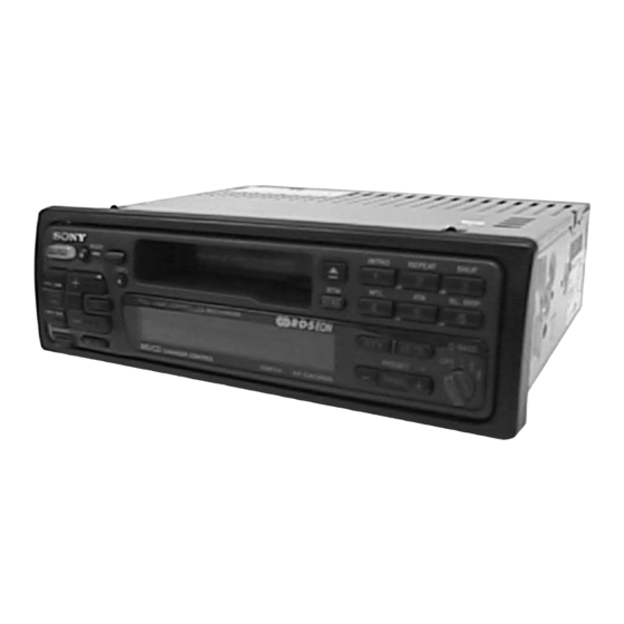
FM/MW/LW CASSETTE CAR STEREO
co
.
9 4
2 8
East European Model
XR-C450RDS
MG-25B-136
Telephone mute control lead
0 5
Power amplifier control lead
8
2 9
9 4
2 8
Power antenna control lead
Line out (1)
Bass ± 8 dB at 100 Hz
Treble ± 8 dB at 10 kHz
12 VDC car battery (negative ground)
Approx. 188 × 58 × 181 mm (w/h/d)
Approx. 182 × 53 × 164 mm (w/h/d)
Approx. 1.2 kg
Parts for installation and connections (1 set)
Rotary commander RM-X2S (1)
Front panel case (1)
m
9 9
9 9
Advertisement
Table of Contents

Related Manuals for Sony XR-C453RDS


Summary of Contents for Sony XR-C453RDS
- Page 1 XR-C453RDS 3 7 63 1515 0 SERVICE MANUAL East European Model Ver 1.1 2001.06 For RM-X2S (Remote Commander), please refer to RM-X2S/X3S Service Manual (9-960-039-S) previously issued. Model Name Using Similar Mechanism XR-C450RDS Tape Transport Mechanism Type MG-25B-136 SPECIFICATIONS...
-
Page 2: Table Of Contents
http://www.xiaoyu163.com 3 7 63 1515 0 TABLE OF CONTENTS SERVICING NOTES GENERAL Flexible Circuit Board Repairing • Keep the temperature of the soldering iron around 270 ˚C during Location of Controls ............3 Setting the Clock ............. 3 repairing. • Do not touch the soldering iron on the same conductor of the Using the Rotary Remote .......... - Page 3 http://www.xiaoyu163.com SECTION 1 This section is extracted from instruction manual. GENERAL 3 7 63 1515 0 L 13942296513 u163 – 3 – http://www.xiaoyu163.com...
- Page 4 http://www.xiaoyu163.com 3 7 63 1515 0 L 13942296513 u163 – 4 – http://www.xiaoyu163.com...
- Page 5 http://www.xiaoyu163.com 3 7 63 1515 0 L 13942296513 u163 – 5 – http://www.xiaoyu163.com...
- Page 6 http://www.xiaoyu163.com 3 7 63 1515 0 L 13942296513 u163 – 6 – http://www.xiaoyu163.com...
- Page 7 http://www.xiaoyu163.com 3 7 63 1515 0 L 13942296513 u163 – 7 – http://www.xiaoyu163.com...
- Page 8 http://www.xiaoyu163.com 3 7 63 1515 0 L 13942296513 u163 – 8 – http://www.xiaoyu163.com...
-
Page 9: Disassembly
http://www.xiaoyu163.com SECTION 2 DISASSEMBLY 3 7 63 1515 0 Note: Follow the disassembly procedure in the numerical order given. FRONT PANEL ASS’Y 1 Push the button (release) 2 Remove the front panel ass’y to the direction of the arrow A . L 13942296513 COVER ASS’Y 3 cover ass’y... - Page 10 http://www.xiaoyu163.com 3 7 63 1515 0 SUB PANEL, MECHANISM DECK (MG-25B-136) 5 screw (PTT2.6 × 6) 3 connector (CN352) 6 mechanism deck (MG-25B-136) 4 flexible flat cable (CN351) 2 sub panel 1 three screws (PTT2.6 × 8) L 13942296513 1 three screws 4 eight screws (PTT2.6 ×...
-
Page 11: Assembly Of Mechanism Deck
http://www.xiaoyu163.com SECTION 3 ASSEMBLY OF MECHANISM DECK 3 7 63 1515 0 Note: Follow the assembly procedure in the numerical order given. HOUSING 7 Hold the hanger by bending the claw. 5 Fit projection on C part. 1 Install the catch to the hanger. 2 Install the hanger onto two claws of the housing. - Page 12 http://www.xiaoyu163.com 3 7 63 1515 0 LEVER (LDG-A) / (LDG-B) shaft B shaft A shaft A shaft C shaft C 1 Fit the lever (LDG-A) on shafts A – C and install it. 4 type-E stop ring 2.0 2 Pull the lever in the arrow direction.
- Page 13 http://www.xiaoyu163.com 3 7 63 1515 0 GUIDE (C) 2 guide (C) 1 three claws L 13942296513 u163 – 13 – http://www.xiaoyu163.com...
-
Page 14: Mechanical Adjustments
http://www.xiaoyu163.com SECTION 5 SECTION 4 ELECTRICAL ADJUSTMENTS MECHANICAL ADJUSTMENTS 3 7 63 1515 0 PRECAUTION TEST MODE 1. Clean the following parts with a denatured-alcohol-moistened This set have the test mode function. In the test mode, FM Auto swab: Scan/Stop Level and MW Auto Scan/Stop Level adjustments can playback head pinch roller be performed easier than it in ordinary procedure. -
Page 15: Tuner Section
http://www.xiaoyu163.com 3 7 63 1515 0 FM Stereo Separation Adjustment TUNER SECTION 0 dB=1 µV Setting: SOURCE button: FM Cautions during repair When the tuner unit is defective, replace it by a new one FM RF signal level meter antenna jack (J1) generator because its internal block is difficult to repair. - Page 16 http://www.xiaoyu163.com 3 7 63 1515 0 FM Signal Meter Adjustment MW Auto Scan/Stop Level Adjustment Setting: Setting: SOURCE button: FM SOURCE button: MW FM RF signal 30 Ω 15 pF generator antenna jack (J1) 0.01 µ F 65 pF AM RF signal Carrier frequency : 98.00 MHz generator : 35 dB (56.2 µ...
- Page 17 http://www.xiaoyu163.com 3 7 63 1515 0 Adjustment Location: – SET UPPER VIEW – Tape Speed Adjustment RV1 MW Auto Scan/Stop Level Adjustment RV2 FM Auto Scan/Stop Level Adjustment RV4 FM Stereo Separation Adjustment RV1 FM Signal Meter Adjustment L 13942296513 u163 –...
-
Page 18: Diagrams
http://www.xiaoyu163.com SECTION 6 DIAGRAMS 3 7 63 1515 0 • IC Block Diagrams – MAIN section – IC1 TB2114F (EL) 24 23 21 20 14 13 RIPPLE FILTER – – SEEK/RECP SEEK/RECP 4BIT SWALLOW MODULAS COUNTER PRESCALER 12BIT PHASE PROGRAMABLE COMPARATOR COUNTER REFERENCE... - Page 19 http://www.xiaoyu163.com 3 7 63 1515 0 IC151 LC75373ED – LFIN – – – LFOUT – LSELO LROUT – – – VREF SHIFT DECODER LATCH CONTROL REGISTER – – – RROUT RSELO – RFOUT – – – – RFIN 6 7 8 9 10 L 13942296513 IC351 CXA2509AQ-T4...
- Page 20 http://www.xiaoyu163.com 3 7 63 1515 0 IC601 BA3918-V2 IC701 BA8270F-E2 BUS ON BUS ON SWITCH REGULATOR RESET SWITCH BUS ON CLK IN BATTERY BATT BU IN SWITCH OVER VOLTAGE PROTECT VREF DATA IN – DATA DATA OUT 2 3 4 •...
-
Page 21: Printed Wiring Board - Main Section
XR-C453RDS 6-1. PRINTED WIRING BOARD – MAIN SECTION – 3 7 6 3 1 5 1 5 0 • Semiconductor Location Ref. No. Location Ref. No. Location D703 E-10 D704 D-10 F-10 D705 D-10 D150 D706 C-10 D151 D152... -
Page 22: Schematic Diagram – Main Section (1/2)
XR-C453RDS 6-2. SCHEMATIC DIAGRAM – MAIN SECTION (1/2) – • See page 18 to for IC Block Diagrams, see page 20 for waveforms, see page 37 for IC Pin Function Description. 3 7 6 3 1 5 1 5 0... - Page 23 http://www.xiaoyu163.com 3 7 63 1515 0 Note on Schematic Diagram: •Semiconductors Operation Name • All capacitors are in µF unless otherwise noted. pF: µµF 50 Ref. No. Operation Name WV or less are not indicated except for electrolytics and tantalums. FM/AM PLL •...
- Page 24 • All resistors are in Ω and W or less unless otherwise IC601 Regulator specified. IC701 Bus Interface (for SONY bus) • : panel designation. • : B+ Line. Regulator control switch • Power voltage is dc 14.4 V and fed with regulated dc power...
-
Page 25: Schematic Diagram - Main Section (1/2)
XR-C453RDS 3 7 6 3 1 5 1 5 0 6-3. SCHEMATIC DIAGRAM – MAIN SECTION (2/2) – • See page 18 for IC Block Diagrams. 1 3 9 4 2 2 9 6 5 1 3 w w w u 1 6 3 –... -
Page 26: Printed Wiring Board - Power Section
XR-C453RDS 3 7 6 3 1 5 1 5 0 6-4. PRINTED WIRING BOARD – POWER SECTION – • Semiconductor Location 1 3 9 4 2 2 9 6 5 1 3 Ref. No. Location D801 D813 D814 D815... -
Page 27: Schematic Diagram - Power Section
XR-C453RDS 3 7 6 3 1 5 1 5 0 6-5. SCHEMATIC DIAGRAM – POWER SECTION– Note on Schematic Diagram: • All capacitors are in µF unless otherwise noted. pF: µµF 50 WV or less are not indicated except for electrolytics and tantalums. -
Page 28: Printed Wiring Board - Display Section
XR-C453RDS 3 7 6 3 1 5 1 5 0 6-6. PRINTED WIRING BOARD – DISPLAY SECTION – 1 3 9 4 2 2 9 6 5 1 3 • Semiconductor Location Ref. No. Location Note on Printed Wiring Board: D901 •... -
Page 29: Schematic Diagram - Display Section
XR-C453RDS 3 7 6 3 1 5 1 5 0 6-7. SCHEMATIC DIAGRAM – DISPLAY SECTION – 1 3 9 4 2 2 9 6 5 1 3 Note on Schematic Diagram: • All capacitors are in µF unless otherwise noted. pF: µµF 50 WV or less are not indicated except for electrolytics and tantalums. -
Page 30: Ic Pin Function Description
Key acknowledge signal input pin – VOLSO Data output pin to electrical volume BUSON BUS ON control signai output pin (for SONY BUS) VOLCKO Clock output pin to electrical volume SYSRST System reset signal output pin 1 3 9 4 2 2 9 6 5 1 3... -
Page 31: Tel 13942296513
http://www.xiaoyu163.com SECTION 7 EXPLODED VIEWS 3 7 63 1515 0 NOTE: • Items marked “*” are not stocked since they • -XX and -X mean standardized parts, so they may have some difference from the original one. are seldom required for routine service. Some •... - Page 32 3-009-298-01 BUTTON (R) (PTY. AF/TA. - DISK +) 3-009-304-01 BUTTON (RELEASE) * 114 3-010-282-01 PLATE (LCD), GROUND 3-932-475-01 SPRING (RELEASE) * 115 3-009-305-11 SHEET (REFLECTOR) 3-904-194-01 EMBLEM (NO. 2.5), SONY * 116 3-009-302-01 PLATE (LCD), LIGHT GUIDE X-3374-107-1 PANEL ASSY * 117 3-009-303-02 HOLDER (LCD) u163...
- Page 33 http://www.xiaoyu163.com 3 7 63 1515 0 (3) MECHANISM DECK SECTION (MG-25B-136) HP901 M901 L 13942296513 Ref. No. Part No. Description Remark Ref. No. Part No. Description Remark A-3291-667-A CLUTCH (FR) ASSY 3-008-874-02 CATCHER 3-701-437-21 WASHER 3-933-344-01 GUIDE (C) * 203 3-008-883-01 LEVER (LDG-A) 3-014-798-01 SCREW (HEAD), SPECIAL * 204...
-
Page 34: Electrical Parts List
http://www.xiaoyu163.com SECTION 8 ELECTRICAL PARTS LIST 3 7 63 1515 0 NOTE: • Items marked “*” are not stocked since they • Due to standardization, replacements in the When indicating parts by reference number, please include the board. parts list may be different from the parts speci- are seldom required for routine service. - Page 35 http://www.xiaoyu163.com MAIN 3 7 63 1515 0 Ref. No. Part No. Description Remark Ref. No. Part No. Description Remark R922 1-216-045-00 METAL CHIP 1/10W 1-163-037-11 CERAMIC CHIP 0.022uF R923 1-216-045-00 METAL CHIP 1/10W R924 1-216-049-11 METAL CHIP 1/10W 1-164-161-11 CERAMIC CHIP 0.0022uF 10% 100V R925...
- Page 36 http://www.xiaoyu163.com MAIN 3 7 63 1515 0 Ref. No. Part No. Description Remark Ref. No. Part No. Description Remark C221 1-126-157-11 ELECT 10uF C704 1-164-004-11 CERAMIC CHIP 0.1uF C222 1-163-251-11 CERAMIC CHIP 100PF C223 1-163-251-11 CERAMIC CHIP 100PF < CONNECTOR/JACK > C224 1-126-096-11 ELECT 10uF...
- Page 37 http://www.xiaoyu163.com MAIN 3 7 63 1515 0 Ref. No. Part No. Description Remark Ref. No. Part No. Description Remark JC63 1-216-296-00 CONDUCTOR, CHIP (3216) < IC > JC65 1-216-296-00 CONDUCTOR, CHIP (3216) JC66 1-216-296-00 CONDUCTOR, CHIP (3216) 8-759-448-88 IC TB2114F(EL) JC67 1-216-296-00 CONDUCTOR, CHIP (3216) 8-759-163-63 IC TDA7330BD-013TR...
- Page 38 http://www.xiaoyu163.com MAIN 3 7 63 1515 0 Ref. No. Part No. Description Remark Ref. No. Part No. Description Remark 1-216-057-00 METAL CHIP 2.2K 1/10W R501 1-216-097-00 METAL CHIP 100K 1/10W 1-216-049-11 METAL CHIP 1/10W R505 1-216-049-11 METAL CHIP 1/10W R506 1-216-109-00 METAL CHIP 330K 1/10W...
- Page 39 http://www.xiaoyu163.com MAIN POWER 3 7 63 1515 0 Ref. No. Part No. Description Remark Ref. No. Part No. Description Remark R620 1-216-025-00 METAL CHIP 1/10W R621 1-216-025-00 METAL CHIP 1/10W D823 8-719-970-02 DIODE 1SR139-400 D824 8-719-970-02 DIODE 1SR139-400 R624 1-249-383-11 CARBON 1/6W D825 8-719-970-02 DIODE 1SR139-400...
- Page 40 http://www.xiaoyu163.com 3 7 63 1515 0 Ref. No. Part No. Description Remark ************************************************************ ************** HARDWARE LIST ************** 7-621-772-10 SCREW +B 2X4 7-685-793-09 SCREW +PTT 2.6X8 (S) 7-685-792-09 SCREW +PTT 2.6X6 (S) 7-685-106-19 SCREW +P 2X10 TYPE2 NON-SLIT 7-624-104-04 STOP RING 2.0, TYPE-E 7-627-553-17 PRECISION SCREW +P 2X2 TYPE 3 ************************************************************ ACCESSORIES &...
- Page 41 XR-C453RDS 3 7 63 1515 0 East European Model SERVICE MANUAL Ver 1.1 2001.06 SUPPLEMENT-1 File this supplement with the service manual. Subject: MAIN Board Modification (SPM-01012) In this set, following board has been changed in the midway of production.
- Page 42 XR-C453RDS 3 7 63 1515 0 DIAGRAMS 2-1. NOTE FOR PRINTED WIRING BOARD AND SCHEMATIC DIAGRAMS Note on Printed Wiring Board: Note on Schematic Diagram: • X : parts extracted from the component side. • All capacitors are in µF unless otherwise noted. pF: µµF •...
- Page 43 3 7 6 3 1 5 1 5 0 • Semiconductor Location Ref. No. Location CN701 CNJ150 BUS CONTROL IN BUS AUDIO LINE OUT (FOR SONY BUS) REAR (ORIGINAL SERVICE MANUAL Page 29) (ORIGINAL SERVICE MANUAL Page 30) G-14 POWER BOARD POWER BOARD CN803 CN802 D150...
- Page 44 XR-C453RDS 3 7 6 3 1 5 1 5 0 2-3. SCHEMATIC DIAGRAM – MAIN Board (1/3) – FM/AM TUNER UNIT (TUX-006/2(EE)) CNJ150 BUS AUDIO IN LINE OUT REAR C124 R118 R151 C151 C153 25V 3.3k 4.7k 0.47 0.022...
- Page 45 XR-C453RDS 3 7 6 3 1 5 1 5 0 2-4. SCHEMATIC DIAGRAM – MAIN Board (2/3) – (Page 4) C408 C308 R408 JC58 R351 R305 C305 R307 C309 330k 0.22 2.2k 1000p C410 2200p R303 R308 C310 JC18...
- Page 46 MA8068-H BATTERY CHECK Q610 2SC2412K-QR C701 D605 C610 R607 0.022 MA8056-M D701 MA8180-M R603 C612 CN701 BUS CONTROL IN (FOR SONY BUS) R708 JC33 R704 UNISI 100k UNISO JC34 BUS.ON B.DATA w w w UNICLK B.CLK BUSON JC35 JC79 D703...
- Page 47 XR-C453RDS 3 7 63 1515 0 MAIN 3. ELECTRICAL PARTS LIST NOTE: • Items marked “*” are not stocked since they • Due to standardization, replacements in the When indicating parts by reference number, please include the board. parts list may be different from the parts speci- are seldom required for routine service.
- Page 48 XR-C453RDS MAIN 3 7 63 1515 0 Ref. No. Part No. Description Remark Ref. No. Part No. Description Remark C351 1-163-251-11 CERAMIC CHIP 100PF < DIODE > C353 1-124-465-00 ELECT 0.47uF 8-719-991-65 DIODE SB02W03C C354 1-163-021-11 CERAMIC CHIP 0.01uF...
- Page 49 XR-C453RDS 3 7 63 1515 0 MAIN Ref. No. Part No. Description Remark Ref. No. Part No. Description Remark J501 1-566-822-41 JACK (REMOTE IN) JC79 1-216-296-00 CONDUCTOR, CHIP JC80 1-216-296-00 CONDUCTOR, CHIP < CHIP CONDUCTOR > JC81 1-216-296-00 CONDUCTOR, CHIP 1-216-295-00 CONDUCTOR, CHIP <...
- Page 50 XR-C453RDS MAIN 3 7 63 1515 0 Ref. No. Part No. Description Remark Ref. No. Part No. Description Remark R110 1-216-077-00 METAL CHIP 1/10W R521 1-216-246-00 METAL CHIP 100K 1/8W R111 1-216-077-00 METAL CHIP 1/10W R522 1-216-097-00 METAL CHIP...
- Page 51 XR-C453RDS 3 7 63 1515 0 MAIN Ref. No. Part No. Description Remark Ref. No. Part No. Description Remark < VARIABLE RESISTOR > 1-241-768-11 RES, ADJ, CARBON 220K < SWITCH > S601 1-692-431-21 SWITCH, TACTILE (RESET) < TUNER UNIT >...
- Page 52 XR-C453RDS 3 7 63 1515 0 REVISION HISTORY Clicking the version allows you to jump to the revised page. Also, clicking the version at the upper right on the revised page allows you to jump to the next revised page.
Need help?
Do you have a question about the XR-C453RDS and is the answer not in the manual?
Questions and answers