Table of Contents
Advertisement
Quick Links
This service information is designed for experienced repair technicians only and is not designed for use by the general public. It does not
contain warnings or cautions to advise non-technical individuals of potential dangers in attempting to service a product.
Products powered by electricity should be serviced or repaired only by experienced professional technicians. Any attempt to service or
repair the product or products dealt with in this service manual by anyone else could result in serious injury or death.
Issue 1
Revision 0
EB-GD67
Frequency Range
Tx/Rx frequency
separation
RF Channel Bandwidth
Number of RF channels
Speech coding
Operating temperature
Type
RF Output Power
Modulation
Connection
Voice digitizing
Transmission speed
Signal Reception
Antenna Impedance
(External Connector)
Antenna VSWR
Dimensions
Volume
Weight
Display
Illumination
Keys
SIM
External DC Supply
Voltage
Battery
Standby Time
Talk Time
Talk and standby time will be dependent on network conditions, SIM card, backlight usage
and network condition.
WARNING
© 2002
Development of Europe Ltd. All rights reserved.
Unauthorized copying and distribution is a violation
of law.
Order Number: MMCD020801C8
Digital Cellular Phone
900 MHz
Tx: 880 - 915MHz
Tx: 1710 -1785 MHz
Rx: 925 - 960 MHz
Rx: 1805 -1880 MHz
45 MHz
95 MHz
200 kHz
174
374
Full rate/Half rate/Enhanced Full rate
-10 °C to +55 °C
Class 4 Handheld
Class 1 Handheld
2 W maximum
1 W maximum
GMSK (BT = 0.3)
8 ch / TDMA
13 kbps RPE-LTP / 13 kps ACLEP / 5.6 kps CELP / VSLEP
270.833 kbps
Direct conversion
50 Ω
< 2.1 : 1
Height: 109 mm
Width:
45 mm
Depth:
20 mm
81 cc
81 g
Graphical chip on glass liquid crystal, Alphanumeric,
101 x 80 pixels, 256-colour palette (RGB).
8 LEDs for Keypad Backlighting (Green)
1 LED for LCD Backklighting (White)
2 LEDs for Incoming call (Green) and Charging (Red)
16-key Keypad, Navigation key.
3 V Plug-in type only
5.8 V
3.7 V nominal, 690mAh, Li-Ion
60 - 190 hrs
1.5 - 6.5 hrs
Matsushita
Mobile
1800 MHz
Communications
Advertisement
Table of Contents

Related Manuals for Panasonic EB-GD67


Summary of Contents for Panasonic EB-GD67
- Page 1 Order Number: MMCD020801C8 Digital Cellular Phone EB-GD67 1800 MHz 900 MHz Frequency Range Tx: 880 - 915MHz Tx: 1710 -1785 MHz Rx: 925 - 960 MHz Rx: 1805 -1880 MHz Tx/Rx frequency 45 MHz 95 MHz separation RF Channel Bandwidth...
-
Page 2: Table Of Contents
COMPANY LIABILITY Every care has been taken to ensure that the contents of this manual give an accurate representation of the equipment. However, Matsushita Mobile Communications Development of Europe Ltd. accepts no responsibility for inaccuracies which may occur and reserves the right to make changes to the specification or design without prior notice. The information contained in this manual and all rights in any design disclosed therein, are and remain the exclusive property of Matsushita Mobile Communications Development of Europe Ltd. -
Page 3: Introduction
1.1. Purpose of this Manual This Service Manual contains the information and procedures required for installing, operating and servicing the Panasonic GSM Personal Cellular Mobile Telephone system operating on GSM Digital Cellular Networks. -
Page 4: General Description
This section provides a general description and kit composition details for the Digital Cellular Phone and optional kits. 2.2. Features The Panasonic Phone Model GD67 is a high performance, small, light, telephone handset for business and domestic use on General Packet Radio Service (GPRS) running on GSM networks. The following features are provided: •... -
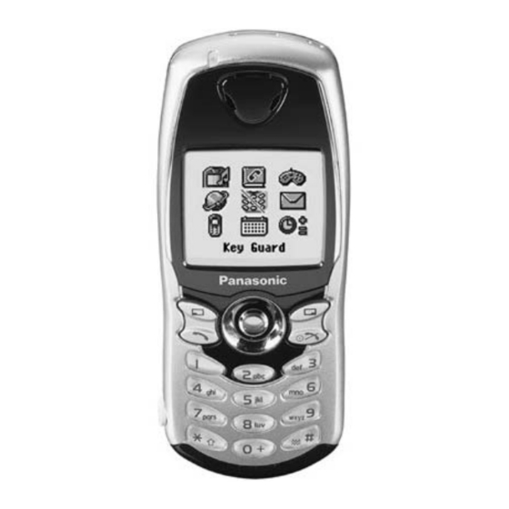
Page 5: Operating Instructions
OPERATING INSTRUCTIONS 3 OPERATING INSTRUCTIONS 3.1. General This section provides a brief guide to the operation and facilities available on the telephone handset. Refer to the Operating Instructions supplied with the telephone for full operational information. 3.2. Liquid Crystal Display The telephone handset has a graphical chip on glass display. -
Page 6: Location Of Controls
OPERATING INSTRUCTIONS 3.3. Location of Controls Incoming / Charge indicator: Green - Incoming call. Red - Charging battery pack. External connector: Used to connect to external accessories or to charging equipment. EARPIECE INCOMING CALL / CHARGE INDICATOR NAVIGATION KEY COVER (EXTERNAL CONNECTOR) EARPHONE / MICROPHONE SOCKET... -
Page 7: Concept Of Operation
OPERATING INSTRUCTIONS 3.4. Concept of Operation There is a close relationship between the Select keys, Navigation key and display. SECONDARY MAIN OPTION AREA OPTION AREA SELECT KEY SELECT KEY NAVIGATION 10626-1 Figure 3.3: Concept of Operation Pressing up and down ( ) will move the pointer up and down and scroll through more information in the main area of the display. -
Page 8: Features Menu Structure
OPERATING INSTRUCTIONS 3.5.2 Editing Alpha Entry Pressing will move the cursor up or down one line. Pressing will move the cursor left or right one character. When the cursor is moved over a character and another key pressed this will insert the new character. Pressing will delete the character to the left of the cursor. -
Page 9: Technical Description
TECHNICAL DESCRIPTION 4 TECHNICAL DESCRIPTION 4.1. RF Overview 4.1.1 General Specifications The telephone is a Dual Band product incorporating two switchable transceivers, one for the E-GSM 900 band and another for the GSM 1800 (DCS 1800) band. The transmit and receive bands for the mobile are given in the table below: E-GSM 900 880-915 MHz 925-960 MHz... -
Page 10: Transmitter
TECHNICAL DESCRIPTION 4.2. Transmitter 4.2.1 Functional Description U200 U203 ÷4 U205 S201 DUAL BAND BUFFER AMP ANTENNA SWITCH FL201 MODULE E100 EGSM 900 EGSM 900 ÷2 FILTER RF TP / SWITCH E101 GSM 1800 GSM 1800 DUAL BAND ATTENUATOR U202 TRANSCEIVER (PART) 10577-1 Figure 4.1: Transmitter Block Diagram... -
Page 11: Receiver
TECHNICAL DESCRIPTION 4.3. Receiver 4.3.1 Functional Description FL203 S201 U200 Rx SAW SWITCH DUAL BAND TRANSCEIVER FILTERS MODULE BASEBAND FILTERS EGSM 900 BASEBAND TEST AMPLIFIERS GSM 1800 10576-1 Figure 4.2: Receiver Block Diagram The main building block for the receiver is the dual band transceiver IC (U200) which includes a direct conversion receiver with I and Q quadrature demodulation. -
Page 12: Baseband Overview
TECHNICAL DESCRIPTION 4.4. Baseband Overview 4.4.1 Introduction The Baseband circuits of the phone are required to perform the following functions: • Equalisation • Channel coding / decoding • Speech coding / decoding • Data Encryption • Layer 1, 2 and 3 software tasks •... - Page 13 TECHNICAL DESCRIPTION 4.4.2 Keypad The Keypad has a 5 x 5 matrix, allowing 25 keys to be scanned. When a key being pressed, a keypad interrupt is generated. To find which key has been pressed, the software scans each column in turn and reads which row is active. Because of key bounce, the key press is confirmed twice at approximately 20 ms intervals.
-
Page 14: Cpu Memory
TECHNICAL DESCRIPTION 4.4.4 The TPU provides the GSM TPU TDMA timing requirements for the system. TPU Timing output signal assignments of CALYPSO Name Ball No. Function Connection Configuration TSPACT 0 PAON External Used for triggering Measuring Equipment TSPACT 1 PLLON TSPACT 2 TSPACT 3 TSPACT 4... -
Page 15: Accessory Interface
TECHNICAL DESCRIPTION 4.4.7 Real Time Clock (RTC) Clock functions are provided by a Real Time Clock built into CALYPSO. The module is synchronised by a 32.768 kHz crystal and is powered via a dedicated regulator in IOTA and is backed up by a 2.5 V button battery. CALYPSO has a clock auto compensation function to take into account any inaccuracies of the crystal. -
Page 16: Power Supplies
TECHNICAL DESCRIPTION 4.5. Power Supplies 4.5.1 Introduction U620 R625 VBACKUP IOTA VBAT D621 BACKUP MAIN CELL BATTERY BAT-TEMP VRRAM D28VR U640 FLASH VRMEM D28V + SRAM D28VB VRIO U751 MELODY VRABB U600 GENERATOR A28V CALYPSO VBAT HEADSET VRBB D18V Q781 ONOFF SPEAKER ACC-PWR... -
Page 17: Voltage Regulation
TECHNICAL DESCRIPTION 4.5.3 Power On / Off Control The power on sequence can begin when VBAT >2.6 V or VBACKUP >2.6 V. In this state IOTA (U620) is in Power On Condition and internal supply UPR is active. RESPWRONZ signal to CALYPSO (U642) is released high. If IOTA is in the Power On Condition, one of following conditions start the Power Up sequence. - Page 18 TECHNICAL DESCRIPTION • VRMEM: Power supply used by Baseband Digital part. Voltage 2.8 V ±0.1 V Current 60 mA max. Dropout 100 mV max (load max) Supply VBAT Supplies CALYPSO memory interface and external memory components. Selectable between 1.8 V and 2.8 V. •...
-
Page 19: Backup Battery
Over Voltage Protection As the accessory connector CN780 is unique to Panasonic, only approved chargers can be used with the handset. Therefore, no additional circuitry is required within the handset to prevent the charger voltage exceeding the design limit of 7 V. - Page 20 TECHNICAL DESCRIPTION 4.5.8 Accessory Control The telephone can detect accessories connected to the I/O connector by pulsing ACC_PWR high and checking DATA_MODE0 and DATA_MODE1. It can then communicate with the detected peripheral and control set ACC_PWR where required, as detailed in the following table. Inputs (Pin No.) Outputs Peripherals...
-
Page 21: Disassembly / Reassembly
DISASSEMBLY / REASSEMBLY INSTRUCTIONS 5 DISASSEMBLY / REASSEMBLY INSTRUCTIONS 5.1. General This section provides disassembly and reassembly procedures for the main components of the telephone. These assemblies MUST be performed by qualified service personnel at an authorised service centre. The following Warnings and Cautions MUST be observed during all disassembly / reassembly operations: WARNING The equipment described in this manual contains polarised capacitors utilising liquid electrolyte. -
Page 22: Disassembly
DISASSEMBLY / REASSEMBLY INSTRUCTIONS 5.2. Disassembly 5.2.1. Case Removal Press down on (A) to allow the I/O Connector Cover to open, thus releasing the Battery Cover (B). Gently lift up the Battery Cover. 10587-1 Slide the Battery Hook in the direction indicated by the arrow. - Page 23 DISASSEMBLY / REASSEMBLY INSTRUCTIONS Starting on one side of the phone, release tags ‘A’, ‘B’ and ‘C’. 10. Continue by releasing tags ‘A’, ‘B’, ‘C’ on the opposite side of the phone before separating the case and cover at tab ‘D’. 10590-1 11.
- Page 24 DISASSEMBLY / REASSEMBLY INSTRUCTIONS 5.2.3. Case-Mounted Components Remove the keypad by pressing on the navigation key until the membrane can be peeled away from the case front. 10593-1 Remove the microphone assembly by prising upward with a small pair of tweezers or similar blunt object through the slot in the side of the microphone holder.
-
Page 25: Reassembly
DISASSEMBLY / REASSEMBLY INSTRUCTIONS Apply pressure to lugs A and B in direction shown to release the antenna from the case. 10598-1 5.3. Reassembly Reassembly is the reverse of disassembly. IF ANY OF THE RF OR LOGIC SHIELDS ARE REMOVED FROM THE PCB AT ANY TIME, THEY MUST BE REPLACED BY NEW ITEMS. -
Page 26: Revision 0
REPAIR PROCEDURES 6 REPAIR PROCEDURES 6.1. Introduction This section provides information on testing the telephone. The layout is as follows: Section 6.2: Lead Free (PbF) solder: Identification and repair of PCBs using Pbf solder. Section 6.3 External testing: describes equipment requirements and general set up procedure. Section 6.4 Complete Unit Test Setup: describes how the items of test equipment are used together and general set up procedure. -
Page 27: Power Supply
REPAIR PROCEDURES 4 . 8 . 2 8 FRONT REAR 10016-1 Figure 6.1: Interface Box IFB003 / IFB004 Personal Computer (PC) The PC (IBM compatible) is used as a Unit Under Test controller. This, in conjunction with the channel box software, allows all of the test facilities normally provided through the keypad of the Unit Under Test. - Page 28 REPAIR PROCEDURES Dummy Battery (Part No. JT00083) The dummy battery is used for baseband calibration and to power the phone without a battery. It is powered from the Interface Box. It differs from previous models in that it obviates the need for a Battery Calibration Voltage Control Unit (BCVCU). 10619-1 Figure 6.3: Dummy Battery Channel Box Software...
-
Page 29: Test Equipment Setup
RS232 interface cable (9 pin straight through connection) GSM test station. Panasonic Channel Box software for Microsoft Windows ®. The Channel Box software should be installed onto the main drive of the personal computer. The RF cable is connected to the GSM test station via a suitable adaptor. The 12 V supply is connected to the rear socket of the Interface box. - Page 30 Check that the handset is powered-up (LCD is backlit and all LEDs are on). The Channel Box should also display handset IMEI number and Firmware version information in the left-hand column of the screen. A toolbar should also be visible in the top panel where the Panasonic logo is displayed. Figure 6.8: Channel Box Toolbar Additional user instructions are provided in the documentation files supplied with the Channel Box.
-
Page 31: Interfaces And Test Points
INTERFACES AND TEST POINTS 7 INTERFACES AND TEST POINTS 7.1. Interfaces 7.1.1 External I/O CASE FRONT 10570-1 Figure 7.1: External I/O Connector Name HH <==>EXT Function H/H Circuit AGND Audio Ground 10095-2 AUDIO_UP <== not used 10095-2 AUDIO_DN ==> not used 10095-2 DATA MODE0 / <==... - Page 32 INTERFACES AND TEST POINTS Name HH <==>EXT Function H/H Circuit <== RS232C: Request to Send 2.8 V 10582-1 ==> RS232C Clear to Send 10584-1 EXT-PWR <== Power supply for Battery Charge 10585-1 Power supply and digital signal ground 10095-2 7.1.2 LCD Module Interface Connections 10572-1 Figure 7.2: LCD Module Connector...
-
Page 33: Sim Interface
INTERFACES AND TEST POINTS 7.1.3 SIM Interface SIGNAL SIMPWR (3W) SIM_RST SIM_CLK Not connected GROUND CN720 Not connected SIM-I/O Not connected CONN. SIM CONNECTOR (SIM CARD) 10573-1 Figure 7.3: SIM Connection Details 7.1.4 Battery Connector SIGNAL VBAT (+) BAT TEMP GROUND (-) (BATTERY COMPARTMENT) 10574-1... -
Page 34: Test Points
INTERFACES AND TEST POINTS 7.2. Test Points TP No Signal Grid TP211 TCXO-EN TP212 TP703 TP705 TP213 FSYS±BB TP753 TP600 32 kHz CLOCK TP752 TP601 TDO (CALYPSO) TP602 TCK (CALYPSO) TP628 TP603 TP604 nBSCAN TP605 TP620 ONNOFF TP621 D18V TP622 D28VB TP623 D28V... -
Page 35: Calibration Procedures
CALIBRATION PROCEDURES 8 CALIBRATION PROCEDURES 8.1. Introduction NOTE: See Section 6.3. for a list of the equipment and setup procedures required to perform the following adjustment and calibration procedures. The following procedures MUST be performed after replacement or repair of the PCB. Failure to do so may result in incorrect operation of the telephone. - Page 36 CALIBRATION PROCEDURES E-GSM 900 The following table shows the measurement limits according to power level: Output Power (dBm) Power Level Target (PL) Nominal 31.75 31.5 32.0 30.5 30.0 30.8 28.9 28.4 29.4 26.5 27.5 24.5 25.5 22.5 23.5 20.5 21.5 18.5 19.5 16.5...
- Page 37 This procedure requires the use of a Gigatronics 8541C power meter. NOTE: To ensure that the telephone operates within set SAR margins, Panasonic recommends that a power meter capable of measurement to an accuracy of ±0.2 dB is used when calibrating power levels. Use of a less accurate power meter may result in the telephone failing to meet SAR standards.
- Page 38 This procedure is used to adjust or verify each calibration channel in turn. NOTE: To ensure that the telephone operates within set SAR margins, Panasonic recommends that a power meter capable of measurement to an accuracy of ±0.2 dB is used when calibrating power levels. Use of a less accurate power meter may result in the telephone failing to meet SAR standards.
-
Page 39: Rssi
CALIBRATION PROCEDURES 8.2.4. Manual Verification Procedure If the Manual Calibration screen is not already open, carry out steps 1 to 5 of Section 8.2.3 Click on the VERIFY Button. Read the expected power and check against the power-meter value. If the values are not correct, adjust them by clicking on the TRIM button to open the Trim Power Level window. Adjust the slider or enter a new DAC value until the power meter is within the power limits listed in paragraph 8.2.1. -
Page 40: Battery Calibration
CALIBRATION PROCEDURES Repeat steps 4 and 5 until the STEP button is greyed out (i.e. cannot be selected). Click on the EXIT button when finished. 8.4. Battery Calibration 8.4.1 Preliminaries There are two procedures associated with battery calibration, battery temperature and battery voltage. A dummy battery, as listed in Section 6.3.2, is required to perform these checks. - Page 41 CALIBRATION PROCEDURES Set the Interface box to POWER ON, IGN and EXT PWR OFF. With the Channel Box software running, click on the Battery Calibration button The Battery Calibration window is divided into two areas: a) Temperature calibration b) Voltage and Current MDAC calibration. 8.4.2 Temperature Calibration Ensure that VBAT is set to 4.1 V.
- Page 42 CALIBRATION PROCEDURES 8.4.3 Voltage and Current MDAC Calibration On the Interface Box, ensure that the EXT PWR switch is ON. Check that the dummy battery 82 Ohms switch is set to ON. Carry out the instructions described in the main dialogue window. When prompted, measure the dummy battery voltage by connecting a voltmeter to the terminals on the top of the dummy battery.
-
Page 43: Replacement Parts List
REPLACEMENT PARTS LIST 9 REPLACEMENT PARTS LIST 9.1. Case and Cover Parts Ref. No. Part No. Part Name & Description M103 GD67CVR01R GD67 COVER RED, SERVICE GD67CVR01B GD67 COVER BLUE, SERVICE comprising: M105 NAVI PANEL GD67 M117 INDICATOR PIPE GD67 M117 M119 SAR SHIELD GD67... -
Page 44: Sub-Assemblies
PCB ASSY LANGUAGE PACK B GD67BRD001C PCB ASSY LANGUAGE PACK C GD67BRD001D PCB ASSY LANGUAGE PACK D Network-specific (SIM-locked) PCB Assemblies are available - please refer to Panasonic spares representative for details. Issue 1 Section 9 MMCD020801C8 Revision 0 – 42 –... -
Page 45: Pcb Components
REPLACEMENT PARTS LIST 9.4. PCB Components Ref. Part No. Part Name & Description Grid C289 F1H1A1050026 CAP CER 1uF 10% 10V Ref. Part No. Part Name & Description Grid C290 ECJ0EC1H330J CAP CER 33pF 5% 50V NP0 C291 ECJ0EC1H330J CAP CER 33pF 5% 50V NP0 C292 ECJ0EC1H330J CAP CER 33pF 5% 50V NP0... - Page 46 REPLACEMENT PARTS LIST Ref. Part No. Part Name & Description Grid Ref. Part No. Part Name & Description Grid C785 ECJ0EC1H101J CAP CER 100pF 5% 50V NP0 L223 ELJRF4N7DF2 INDUCTOR 4.7nH +/-0.3nH C786 F1G1A104A012 CAP CER 100nF 10% 10V X5R L226 ELJRF12NJF2 INDUCTOR 12nH 5%...
-
Page 47: Refurbishment Kits
REPLACEMENT PARTS LIST Ref. Part No. Part Name & Description Grid Ref. Part No. Part Name & Description Grid R280 ERJ2GE0R00X RES JUMPER 0 OHM 1A R783 ERJ2GEJ103X RES 10K OHM 5% 1/16W R281 ERJ2GEJ101X RES 100 OHM 5% 1/16W R784 ERJ2GEJ104X RES 100K OHM 5% 1/16W... -
Page 48: Document Packs
REPLACEMENT PARTS LIST 9.7. Document Packs Ref. No. Part No. Part Name & Description GD67DPK01 ARABIC GD67DPK02 CZECH GD67DPK03 DANISH, GERMAN, EU WARRANTY GD67DPK04 DANISH, EU WARRANTY GD67DPK05 DUTCH, FRENCH, GERMAN, EU WARRANTY GD67DPK06 DUTCH, EU WARRANTY GD67DPK07 SLOVAK GD67DPK08 FRENCH GD67DPK09 GERMAN, EU WARRANTY... -
Page 49: Circuit Diagrams
CIRCUIT DIAGRAMS 10 CIRCUIT DIAGRAMS Figure 10.1: Circuit Diagram - RF MMCD020801C8 Section 10 Issue 1 Service Manual – 47 – Revision 0... - Page 50 CIRCUIT DIAGRAMS U600 U600 Figure 10.2: Circuit Diagram - Baseband Issue 1 Section 10 MMCD020801C8 Revision 0 – 48 – Service Manual...
- Page 52 CIRCUIT DIAGRAMS Figure 10.4: Circuit Diagram - Audio Interfaces Issue 1 Section 10 MMCD020801C8 Revision 0 – 50 – Service Manual...
- Page 53 CIRCUIT DIAGRAMS Figure 10.5: Circuit Diagram - Peripherals 1 of 2 MMCD020801C8 Section 10 Issue 1 Service Manual – 51 – Revision 0...
- Page 54 CIRCUIT DIAGRAMS Figure 10.6: Circuit Diagram - Peripherals 2 of 2 Issue 1 Section 10 MMCD020801C8 Revision 0 – 52 – Service Manual...
-
Page 55: Layout Diagrams
LAYOUT DIAGRAMS 11 LAYOUT DIAGRAMS Figure 11.1: PCB Layout - Side A MMCD020801C8 Section 10 Issue 1 Service Manual – 53 – Revision 0... - Page 56 LAYOUT DIAGRAMS Figure 11.2: PCB Layout - Side B Issue 1 Section 10 MMCD020801C8 Revision 0 – 54 – Service Manual...
- Page 57 10 CIRCUIT DIAGRAMS Figure 10.1: Circuit D MMCD020801C8 Section 10 Service Manual – 47 –...
- Page 58 CIRCUIT DIAGRAMS 0.1: Circuit Diagram - RF Section 10 Issue 1 – 47 – Revision 0...
- Page 59 CIRCUIT DIAGRAMS U600 U600 Figure 10.2: Circuit Diagram Issue 1 Section 10 Revision 0 – 48 –...
-
Page 60: Mmcd020801C8 Service Manual
rcuit Diagram - Baseband Section 10 MMCD020801C8 – 48 – Service Manual...
Need help?
Do you have a question about the EB-GD67 and is the answer not in the manual?
Questions and answers