Table of Contents
Advertisement
Quick Links
Manual P/N 454-44000
This material contains information of proprietary interest to BVM Ltd. It has been supplied in
confidence and the recipient, by accepting this material, agrees that the subject matter will not be
copied or reproduced, in whole or in part, nor its contents revealed in any manner or to any person
except to meet the purposes for which it was delivered.
User's Manual
BVME4000/6000
MC68040/68060 SINGLE BOARD
COMPUTER
Board Revision F
Manual Revision I 21 February 2001
BVM Limited,
Hobb Lane,
Hedge End,
Southampton,
SO30 0GH, UK.
TEL: +44 (0)1489 780144
FAX: +44 (0)1489 783589
E-MAIL: sales@bvmltd.co.uk
WEB:
http://www.bvmltd.co.uk
Advertisement
Table of Contents

Summary of Contents for BVM BVME4000
- Page 1 Board Revision F Manual Revision I 21 February 2001 This material contains information of proprietary interest to BVM Ltd. It has been supplied in confidence and the recipient, by accepting this material, agrees that the subject matter will not be copied or reproduced, in whole or in part, nor its contents revealed in any manner or to any person except to meet the purposes for which it was delivered.
- Page 2 This page is intentionally left blank.
- Page 3 BVM Ltd. This applies to any merged, modified or derivative version USE OF PRODUCT...
- Page 4 Damage may result if users attempt to remove or fit EPROM's incorrectly. Do not lever out the IP's from the BVME4000/6000. The board uses surface-mounted devices extensively, which can be fractured by excessive force. Damage may result if users attempt to remove or fit IP's incorrectly.
-
Page 5: Table Of Contents
Table Of Contents Contents Page 1. Introduction ............................1 1.1 Scope ............................1 1.2 BVME4000 Part Numbers ......................1 1.3 BVME6000 Part Numbers ......................1 1.4 Memory Module Part Numbers ....................1 2. Overview ............................2 2.1 Board Layout ..........................2 2.2 Features .............................3 2.3 Applications ..........................3 3. - Page 6 5.2.11 LK21 SRAM Backup Selection ..................17 5.2.12 LK22 VMEbus System Controller Enable................17 5.2.13 Configuration Switch ......................18 5.3 Indicators..........................18 5.3.1 Green LED - RUNNING......................18 5.3.2 Red LED - VMEbus Master Access ..................18 6. Connector Pinouts ..........................19 6.1 JP1 &...
- Page 7 7.8.4 Interrupt Controller Registers ....................36 7.8.4.1 VMEIRQ Enable Register ................... 36 7.8.4.2 VMEIRQ Vector Register ..................36 7.8.4.3 VMEIRQ Level Register ..................37 7.8.4.4 LOCIRQ Enable Register..................37 7.8.4.5 ETHIRQ Enable Register ..................37 7.8.4.6 Local IRQ Status Register .................. 38 7.9 IP Controller ..........................39 7.9.1 Overview ..........................
- Page 8 A.15 MEM4SD Memory Module User's Guide................61 A.16 EXP100 Quad IP Expansion User's Manual................61 Appendix B CPU Cache Coherency and Bus Snooping ...............62 B.1 BVME4000 (MC68040) ......................62 B.2 BVME6000 (MC68060) ......................64 Appendix C Memory Module Pinout ......................66 Appendix D IP Expansion Interface Pinout ...................67 Appendix E Thermal Management .......................68...
- Page 9 Figure 18 JP3 Parallel Port Connections ....................19 Figure 19 JP4 Optional 10BaseT Connector ..................20 Figure 20 IP Connector Pin Numbering Viewed from solder side of BVME4000/6000......21 Figure 21 Flat Cable Connector Pin Numbering Viewed from front of JP5........... 21 Figure 22 JP7 CPU Fan Power ......................
- Page 10 viii This page is intentionally left blank.
-
Page 11: Introduction
25/33MHz, VMEbus I/F, ETHERNET, SCSI, IP I/F, 2Mb SRAM Other versions of the BVME4000 are available to special order, where any of the VMEbus I/F, ETHERNET, SCSI & IP I/F may be omitted or 512Kb SRAM fitted. Contact your supplier for details. -
Page 12: Overview
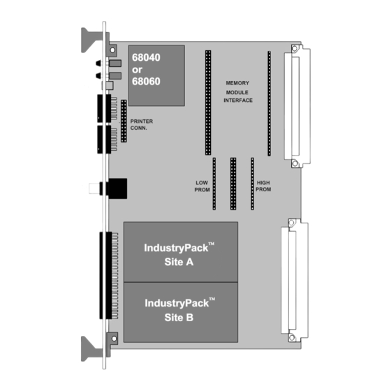
SERIAL CH. A HIGH CHEAPER PROM PROM IndustryPack Site A IP I/O CONN. 2 X 50 WAY VMEbus P2 CONN. IndustryPack Site B Figure 1 Board Layout Copyright 1993,1995,1998,2001 BVM Ltd. -
Page 13: Features
BVME4000/6000 Features BVME4000 - MC68040 CPU (MC68EC040/68LC040 options). " 25 MHz and 33 MHz clock speed variants. " 4096 byte data and instruction caches. BVME6000 - MC68060 CPU (MC68EC060/68LC060 options). " 50 MHz and 66 MHz clock speed variants (25 MHz or 33 MHz bus). -
Page 14: Description
Bus Timers & Timer 14 way Connector IP A IP B EEPROM Parallel I/O 26 way Front Panel Front Panel Centronics Expansion Connector 50 way I/O 50 way I/O Buffers Interface Figure 2 Block Diagram Copyright 1993,1995,1998,2001 BVM Ltd. -
Page 15: Processor
FPU. The MC68LC060/68EC060 can run at 50 or 66MHz with a 25 or 33MHz bus respectively. Memory The BVME4000/6000 may be fitted with a large variety of 32-bit wide, burst fill memory devices. The BVME4000/6000 uses the BVM memory module interface which provides a full 32-bit MC68040/68060... -
Page 16: Serial Communications
5Mbytes per second. The 32-bit DMA driven interface allows direct access to the entire memory map of the BVME4000/6000. The burst mode interface stacks up 16 bytes at a time and transfers them as a line transfer at up to 4/2/2/2 access speeds at 25MHz bus clock. At 5Mbyte/s this gives a 400nS burst every 3.2µS or 12.5% bus bandwidth requirement. -
Page 17: Vmebus Interface
The BVME4000/6000 responds to Byte and Word and Longword Slave accesses to the A32, A24 and A16 address spaces. The BVME4000/6000 can snoop VMEbus slave accesses if enabled to do so. Thus although the CPU uses extensive caching, full coherency is maintained by the CPU providing any data that is 'stale' in the accessed memory - refer to "Appendix B CPU Cache Coherency and Bus Snooping (on page 62)". -
Page 18: Interrupts
3.11 Interrupts 3.11.1 VMEbus Interrupt Handler The BVME4000/6000 may be configured to respond to VMEbus interrupts on any of the 7 VMEbus interrupt levels. Each interrupt level may be programmed to be enabled or disabled individually. A User vectored VMEbus interrupt causes the CPU to reply with a VMEbus Master interrupt acknowledge cycle. -
Page 19: Vmebus System Controller Functions
VMEbus Timeout monitor. 3.15 Configuration Switch A 4-bit configuration switch is provided for software bootstrap detection. This switch does not affect the hardware directly, but is normally used by the software to set up the BVME4000/6000's configuration registers. 3.16 EEPROM... -
Page 20: Installation
BVME4000/6000 Installation The BVME4000/6000 module is inserted into a vacant VMEbus slot. If it is to function as the system controller, then it should be positioned in slot 1. It passes through all VMEbus daisy chained arbitration signals. IACK should be jumpered to IAKIN on the backplane at slot 1. All interrupt IAKIN to IAKOUT and BGIN to BGOUT signals should be jumpered across vacant slots to the right of the module. -
Page 21: Configuration
1 2 3 SWITCH 1 2 3 LK15 DISK POWER CONNECTOR LK13 82596 LANC IP A CONNECTOR BATTERY NCR53C710 SCSI INDUSTRY IP B PACK CONNECTOR CONTROLLER CONTROLLER STATIC RAM SCSI IP EXPANSION Figure 3 PCB Layout Copyright 1993,1995,1998,2001 BVM Ltd. -
Page 22: Link And Switch Definitions
VMEbus connectors to the right. Link positions marked with a # show the default configuration. Some of the link numbers are not described here, these are for factory use only when configuring different build variants of the BVME4000/6000 and are not available for user's. 5.2.1 LK1 Abort Switch Enable... -
Page 23: Lk3 Vmebus Reset Out Enable
Location PERIPHERAL CONTROLLER HIGH PROM PROM This link enables the VMEbus RESET to be driven by the BVME4000/6000 RESET signal. Function 1 & 2 Fitted # BVME4000/6000 RESET resets VMEbus 1 & 2 Omitted NO VMEbus RESET from BVME4000/6000 5.2.4... -
Page 24: Lk5 Cpu Cache Inhibit
Inhibit Location SERIAL B INTERRUPT CONTROLLER This link disables the MC68040/68060's on chip data and instruction caches to allow (for example) emulators to be used with the BVME4000/6000. Function 1 & 2 Fitted MC68040/68060 CACHES DISABLED 1 & 2 Omitted # MC68040/68060 CACHES ENABLED 5.2.6... -
Page 25: Lk7,8,9 Ethernet Aui/Cheapernet Select
2 & 3 2 & 3 AM29F010 / 020 / 040 Write Enable 2 & 3 1 & 2 2 & 3 2 & 3 2 & 3 AM29F010 / 020 / 040 Write Protect Copyright 1993,1995,1998,2001 BVM Ltd. -
Page 26: Lk13 Scsi Termination Disable
Figure 12 LK13 SCSI Termination Disable Location BATTERY This link allows the SCSI bus terminators to be enabled on the BVME4000/6000. This is necessary if the BVME4000/6000 is at the end of the SCSI bus cable, otherwise the terminators should be disabled. -
Page 27: Lk21 Sram Backup Selection
PROM PROM This link forces the BVME4000/6000 to be the VMEbus System Controller, so the BVME4000/6000 performs as the VMEbus arbiter, drives VMEbus SYSCLK and VMEbus BCLR. The normal selection for this function is in the Board Control Register when not overridden by this link - refer to "7.13.3 Port B Usage (on page 52)". -
Page 28: Configuration Switch
RTE instruction, stacking an exception frame or doing an MMU table search. 5.3.2 Red LED - VMEbus Master Access The RED MASTER LED indicates that the BVME4000/6000 is currently an active VMEbus master. Copyright 1993,1995,1998,2001 BVM Ltd. -
Page 29: Connector Pinouts
13 and 21 - 25 unconnected. Figure 17 JP1 & JP2 Serial Port Connections The above assumes standard RS232 drivers are fitted to the BVME4000/6000. If RS422 or RS485 interface modules are fitted refer to the RS422/RS485 INTERFACE MODULE documentation detailed in the "A.9 RS422/485 Interface Module (on page 60)"... -
Page 30: Jp4 Cheapernet Connector
BNC T-piece connected to the BNC connector. The cable is broken at the point of contact and each new end is connected to the T-piece. If the BVME4000/6000 is to be removed from the network, this is simply accomplished by disconnecting the BVME4000/6000 BNC connector (JP4) from the T-piece, leaving the T-piece connected to the cable. -
Page 31: Jp5A/B Ip A/B Connections
JP5A and JP5B on the BVME4000/6000 front panel. The IP I/O connector, the BVME4000/6000 flat cable connectors, and the wires on the ribbon cables are all numbered identically from 1 to 50. -
Page 32: Jp7 Cpu Fan Power
JP8 JTAG Connector JP8 is a JTAG connection via a 2 x 5 way header, the pinout matching the MACH programming lead. This is for factory use only, to program the internal BVME4000/6000 logic devices. /TRST /ENBL Figure 23 JP8 JTAG Connector J1 SCSI Connections J1 carries the SCSI interface signals. -
Page 33: J14 Scsi Peripheral Power Connections
J14 SCSI Peripheral Power Connections J14 provides a power pick up connection for SCSI devices integrated within a module with the BVME4000/6000. It can provide up to 2A of +5V and 2A +12V of +12V. The pinout is arranged to be symmetrical allowing the mating connector to be plugged either way around. -
Page 34: Protection Fuses
The connections on the BVME4000/6000 which provide output power are protected with fuses. These are surface-mounted fuses, and the BVME4000/6000 should be returned to factory for repair if any of these fuses blows. For reference, the following is a list of the fuses, their functions, positions, rating and type. -
Page 35: Programming
Programming Address Map The Address Map for the BVME4000/6000 is shown below. The BVME4000/6000 is byte addressed; each location addresses an 8-bit value. The BVME4000/6000 supports full 32-bit addressing for all four Local Bus Masters (the MC68040/68060 CPU, the 82596CA LANC, the 53C710 SCSI Controller and the VMEbus Slave Interface). -
Page 36: I/O Address Map
Size Memory Module Dependent. The BVME4000/6000 provides a site for BVM Memory Modules - refer to "Appendix C Memory Module Pinout (on page 66)" for details. These modules are available in various configurations (DRAM, SRAM, FLASH) and sizes and access speeds. Refer to the relevant Memory Module documentation detailed in the "Appendix A Data Sheet &... -
Page 37: Vmebus Master Access
BVME4000/6000 VMEbus Master Access The BVME4000/6000 can access VMEbus as a bus master. Depending on the Address Range used, different types of access are performed. VMEbus specifies three basic Address Mode schemes - A16 (Short I/O), A24 (Standard) and A32 (Extended). The BVME4000/6000 supports all of these modes. -
Page 38: A24:D32
Refer to "7.10 VMEbus Slave Access Controller (on page 45)" for RAMLO and VMELO settings. The following Address Modifier (AM) codes are generated: CPU Supervisor Program Access Data Access CPU User Program Access Data Access Copyright 1993,1995,1998,2001 BVM Ltd. -
Page 39: Sram
Size 2Mbyte. The BVME4000/6000 provides 2 x 32-Pin EPROM JEDEC compatible sockets that may be link selected to accept either 64K8, 128K8, 512K8 or 1024K8 EPROM devices (e.g. 27C512, 27C010, 27C020, 27C040 or 27C080), providing 64K-2Mbytes of EPROM or 512K8 AM29F040 single-voltage FLASH EPROM devices, providing 1Mbyte of on-board programmable FLASH EPROM memory. -
Page 40: Scsi Controller
10Mbytes per second. The 32-bit DMA driven interface allows direct access to the entire memory map of the BVME4000/6000. The burst mode interface stacks up 16 bytes at a time and transfers them as a line transfer at up to 4/2/2/2 access speeds at 25MHz bus clock. -
Page 41: Scsi Controller Registers
DSPS DMA SCRIPTS Pointer Save FF000034 SCRATCH General Purpose Scratch Pad FF000038 DCNTL DMA Control FF000039 DMA Watchdog Timer FF00003A DIEN DMA Interrupt Enable FF00003B DMODE DMA Mode FF00003C ADDER Sum Output of Internal Adder Copyright 1993,1995,1998,2001 BVM Ltd. -
Page 42: Scsi Electrical Interface
The SCSI bus requires termination at both ends of the bus. It is important that terminators are fitted at, and only at, both ends of the bus. The BVME4000/6000 uses active, current-mode terminators that provide high performance termination that allows the BVME4000/6000 to achieve 10Mb/s transfer rates when connected to a SCSI-2 bus. -
Page 43: Ethernet Controller
Ethernet (via the AUI interface) and Cheapernet (via a front panel BNC). The 32-bit, DMA driven interface allows direct access to the entire memory map of the BVME4000/6000 allowing full packet management by the 82596CA. Each 32-bit transfer requires 320nS max (including arbitration) to execute the cycle. -
Page 44: Channel Attention Access
7.7.7 Electrical Interface The BVME4000/6000 provides both a full 'Cheapernet' (IEEE802.3 - 10Base2) coaxial interface via the front panel and an Attachment Unit Interface (AUI) port via P2. This allows a transition module to be connected behind the backplane to provide connection to Thick Ethernet (IEE802.3 - 10Base5) or other Ethernet standards (e.g. -
Page 45: Interrupt Controller
If it acknowledges the IP interrupt, then the IP Interface prioritises between any active IP interrupts. When a VMEbus Interrupt is acknowledged, the BVME4000/6000 becomes a VMEbus master and initiates an Interrupt Acknowledge cycle over VMEbus. The BVME4000/6000 expects the VMEbus interrupter to return a vector which is then used by the processor vectoring mechanism. -
Page 46: Vmebus Interrupter
AcKnowledge (ROAK). Thus the interrupt is cleared by the interrupt acknowledge cycle. The BVME4000/6000 may generate an interrupt on any of the seven VMEbus IRQ levels. However, it can only generate on a single level at any one time. The level on which an interrupt is generated is programmable - refer to "7.8.4.2 VMEIRQ Vector Register (below)"... -
Page 47: Vmeirq Level Register
(CLEARing) and re-enabling (SETting) the Ethernet Interrupt. Bit 0: Select Bit. This bit is used to select between the LOCIRQ Enable Register and the ETHIRQ Enable Register. This bit must be written as a ONE to select the ETHIRQ Enable Register. Copyright 1993,1995,1998,2001 BVM Ltd. -
Page 48: Local Irq Status Register
The 82596CA will pulse its interrupt line inactive whenever a 'new' interrupt condition becomes true within the device. Thus to distinguish between an Ethernet Error interrupt and a normal Ethernet interrupt, the ETHERR bit should be interrogated; not the ETHIRQ bit. Copyright 1993,1995,1998,2001 BVM Ltd. -
Page 49: Ip Controller
The IP expansion interface allows for a low cost IP carrier daughter board to be added - refer to "Appendix D IP Expansion Interface Pinout (on page 67)" for details. The BVME4000/6000 contains all the state machine and multiplexing logic thus minimising daughter board circuitry requirements. The interface allows up to four additional IP sites on a daughter board at all speed selections. -
Page 50: Memory Space Address Map
16Mb (D32) IP C/D A23 - A2 F5000000 - F5FFFFFF E6000000 - E6FFFFFF 110x 16Mb (D32) IP E/F A23 - A2 F6000000 - F6FFFFFF E7000000 - E7FFFFFF 111x 16Mb (D32) Reserved don't care F7000000 - F7FFFFFF Copyright 1993,1995,1998,2001 BVM Ltd. -
Page 51: I/O & Id Space Address Map
11XX X 1024 byte Reserved don't care FF801000 - FF8FFFFF XXXX X 1Mbyte minus 4Kbyte Reserved * * NOTE: The address space FF801000 - FF8FFFFF is a wrap-around region of the FF800000 - FF800FFF address space. Copyright 1993,1995,1998,2001 BVM Ltd. -
Page 52: Ip Controller Registers
These bits select on which Interrupt level the IP IntReq will act as an interrupter. The binary code written selects the corresponding interrupt level (e.g. 011 selects level 3). When set to 000 no interrupt can be generated. After RESET these bits are CLEAR (i.e. Interrupt generation disabled). Copyright 1993,1995,1998,2001 BVM Ltd. -
Page 53: Irq Level B1 Register
When SET the IP expansion interface is clocked synchronously with the main CPU clock at either the CPU clock frequency or CPU clock divided by 4 (again dependent on the CLKX bit). After RESET this bit is CLEAR (i.e. 8/32MHz clock selected). Copyright 1993,1995,1998,2001 BVM Ltd. - Page 54 SET the IP expansion interface is clocked synchronously with the main CPU clock at either the CPU clock frequency or CPU clock divided by 4 (again dependent on the CLKA bit). After RESET this bit is CLEAR (i.e. 8/32MHz clock selected). Copyright 1993,1995,1998,2001 BVM Ltd.
-
Page 55: Vmebus Slave Access Controller
7.10.1 Overview The BVME4000/6000 allows other VMEbus masters to access some of its onboard address space. It allows accesses via either A24 or A32 address spaces. The BVME4000/6000 also acts as a location monitor for A16 accesses. 7.10.2 Standard (A24) & Extended (A32) Accesses Both the size of the window and the base address of the window (from the VMEbus master's point of view) are programmable. -
Page 56: Short I/O (A16) Accesses
BVME4000/6000 7.10.3 Short I/O (A16) Accesses The BVME4000/6000 will respond to Short I/O (A16) accesses. The size of the window is fixed at 256bytes. The base address is programmable on 256byte boundaries. Short I/O space accesses act as a location monitor only and do not access physical memory within the BVME4000/6000. -
Page 57: Address Control Registers
A32 (extended) accesses from another VMEbus master. If a bit is set (a 1) then the corresponding address line is ignored. Thus the contents of this register control the size of the window decoded by the BVME4000/6000 - refer to "7.10.4 Controlling The Window Size (on page 46)" for more details. -
Page 58: A24Lba - A24 Local Base Address Register
RAMLO: Map RAM Low. When SET the SRAM (located at E9000000 and F9000000) is also mapped at 00000000. This is mainly intended to provide a common address map for systems with no memory module fitted. Copyright 1993,1995,1998,2001 BVM Ltd. -
Page 59: Configuration Switch
Bit 3-0: SW1, SW2, SW3, SW4. Reflects the state of each numbered switch. When the switch is ON (lower position) the associated bit is read as ZERO. When switch is OFF (upper position) the associated bit is read as ONE. Copyright 1993,1995,1998,2001 BVM Ltd. -
Page 60: Real Time Clock/Timers
7.12 Real Time Clock/Timers 7.12.1 Overview The Real Time Clock and Timer facilities on the BVME4000/6000 are provided by the DP8570A Timer Clock Peripheral, which provides two 16-bit timer/counters, calendar/clock, a flexible interrupt scheme and 44 bytes of non-volatile RAM. -
Page 61: Programming
Day of Week Compare RAM FF900067 Seconds Time Save RAM FF90006B Minutes Time Save RAM FF90006F Hours Time Save RAM FF900073 Day of Month Time Save RAM FF900077 Months Time Save RAM FF90007B FF90007F RAM/TEST Copyright 1993,1995,1998,2001 BVM Ltd. -
Page 62: Parallel Port/Timer
Bit 6: /SYSCON: System Controller Function Enable. This must be programmed as an output pin. This bit controls whether the BVME4000/6000 is the VMEbus System Controller unless overridden by the System Controller Link - refer to "5.2.12 LK22 VMEbus System Controller Enable (on page 17)" for more details. When programmed as the VMEbus System Controller, the BVME4000/6000 performs as the VMEbus arbiter, it drives VMEbus SYSCLK and VMEbus BCLR. - Page 63 BVME4000/6000 Bit 5,4: RQLVL1,RQLVL0: VMEbus Request Level Selection. These must be programmed as output pins. The BVME4000/6000 can request mastership of the VMEbus on any of the four VMEbus request levels. These two bits select which level VMEbus requests are made upon:...
-
Page 64: Port C Usage
PADIR: Port A Direction. This OUTPUT controls the DIRECTION of the transceiver. When SET the transceiver will drive OUT from the BVME4000/6000 to the connector. When CLEAR the transceiver will receive IN from the connector and drive into Port A. -
Page 65: Handshake Pin Usage
This must be configured as an input. It is connected to PBUSY signal via an inverting buffer. This signal is currently not connected on the BVME4000/6000. 7.13.6 MC68230 PI/T Registers The register map of the MC68230 is shown below. The register map consists of a bank of 32 byte wide registers (of which some are undefined). -
Page 66: Serial Communications Controller
PCLK This is the master Z85230 clock pin. It is used to synchronise all internal signals. It is available as a clock source to the baud rate generator. The BVME4000/6000 drives this signal with the processor clock divided by 2. Thus with a 25MHz bus clock, the Z85230 is clocked at 12.5MHz. -
Page 67: Programming
Data Register - Channel B (JP2) FFB0000B Control Register - Channel A (JP1) FFB0000F Data Register - Channel A (JP1) The BVME4000/6000 supports vectored interrupts from the SCC - refer to "7.8 Interrupt Controller (on page 35)" for more details. Copyright 1993,1995,1998,2001 BVM Ltd. -
Page 68: Specifications
BVME4000/6000 Specifications On-Board Functions BVME4000: MC68040, MC68LC040 or MC68EC040 CPU at 25MHz/33MHz. BVME6000: MC68060, MC68LC060 or MC68EC060 CPU at 50MHz/66MHz (25MHz/33MHz bus). Z85230 Dual Serial interface controller, 7.3728MHz or external clock source, RS232 buffers (RS422 & RS485 options), front panel and P2 connections. -
Page 69: Vmebus Interrupts
Note: power requirements exclude IP, Memory Module & Disc Drive power. Environmental: 0 to 70 °C, 95% humidity non-condensing (extended range to order). Refer to "Appendix E Thermal Management (on page 68)" for airflow/heatsink requirements. Copyright 1993,1995,1998,2001 BVM Ltd. -
Page 70: Appendix A Data Sheet & Manual References
MOTOROLA MC68230 PARALLEL INTERFACE/TIMER (PI/T) Data Sheet (Dec 1983). VMEbus Specification THE VMEbus SPECIFICATION (Sept 1987, VITA). RS422/485 Interface Module User's Manual BVM 453-62370/62371 RS422/RS485 INTERFACE MODULE User's Manual (BVM part number: 454- 68370). A.10 AM29F040 Data Book AMD Flash Memory Products Data Book/Handbook 1996. -
Page 71: Nmc24C02 Data Sheet
A.12 MEM390 Memory Module User's Manual MEM390 4/8 Mbyte DRAM MEMORY MODULE User's Manual (BVM part number: 454-68391). A.13 MEM400 Memory Module User's Manual MEM400 16Mbytes DRAM 4/8 Mbytes FLASH MEMORY MODULE User's Manual (BVM part number: 454-61400). A.14 MEM480 Memory Module User's Guide MEM480 16/32/48Mbytes DRAM MEMORY MODULE User's Guide (BVM part number: 454-61480). -
Page 72: Appendix B Cpu Cache Coherency And Bus Snooping
DTT0 = $F00FA040, DTT1 = $00FFA020, ITT0 = NOT USED, ITT1 = $00FFA000 On the BVME4000 with a 68EC040 processor, a similar scheme as that for the 68040/68LC040 can be set up. This gives an I/O region from $F0000000 to $FFFFFFFF for supervisor and user-state access, with the rest of the address space defined as write-through caching for instructions and copyback caching for data for supervisor and user-state access. - Page 73 MMU is used in the 68040 or 68LC040. It is useful to have different regions defined for the same address space, because as the BVME4000 dual-maps some of the address space, it can be accessed in different caching modes. If the above scheme was adopted, then the VMEbus A24 space could be accessed at address $EE000000 as write-through cached, and at address $FE000000 as cache-inhibited bus-serialised access.
-
Page 74: Bvme6000 (Mc68060)
The values that need to be set into the 68EC060 TT registers to implement this scheme are as follows: DTT0 = $F00FC040, DTT1 = $00FFC020,ITT0 = NOT USED, ITT1=$00FFC000 Copyright 1993,1995,1998,2001 BVM Ltd. - Page 75 This does also have a potential performance advantage, as there is a timing overhead involved in bus-snooping by the 68060 processor. Other schemes may be determined by the user, or a combination of the above may be used in conjunction. Copyright 1993,1995,1998,2001 BVM Ltd.
-
Page 76: Appendix C Memory Module Pinout
12 Volt Power NOTES: This allows connection to a BVM Memory Module. # indicates a direct connection to the equivalent processor signal, see the MC68040 and MC68060 manual or data sheet for an explanation. /RST is a general reset signal, /MIRQ is an interrupt signal from the module, and MERR is a bus error signal from the module. -
Page 77: Appendix D Ip Expansion Interface Pinout
This allows connection to a BVM IP Expansion Daughter Board (e.g. EXP100). The BVME4000/6000 architecture provides for a further 6 IP sites to be added via this extension interface. The interface allows full capability sites to be added including Interrupt Control, 32-bit operation 8MHz, 32MHz and CPU Synchronous speeds. -
Page 78: Appendix E Thermal Management
If operation above 50 °C for extended periods is anticipated, then it is recommended that the airflow is doubled, or (where not already specified) a heatsink is fitted. Where a heatsink is specified, fit AAVID part 3325 24 B 0 0032. Copyright 1993,1995,1998,2001 BVM Ltd. -
Page 79: Appendix F Circuit Diagrams
Circuit diagrams are provided here for customer reference only. This information was current at the time this User Manual was last revised. This information is not necessarily current or complete manufacturing data, nor is it part of the product specification. Copyright 1993,1995,1998,2001 BVM Ltd. - Page 80 This is the master sheet for the BVME4000/6000 rev F. Processor and Memory This sheet contains: Industry Pack Interface This sheet contains: Power and Reset This sheet contains: pro_mem.sch ip.sch pwr.sch Processor socket Industry Pack Interface 3.3 V Power Supply...
- Page 81 /ENABLE IC67A IC67D HEADER 5X2 HEADER 10 PST2 GLED /GLED 330R 330R Title + C68 74F38 74F38 BVME4000/60000 10uF BVM Ltd. Issue Dwg No. Size Hobb Lane. BVM00228 Hedge End Southampton Date Sheet 2 of 8 10 December 1998 SO30 0GH...
- Page 82 Fit 2-3 For Enable BRDY SHIELD (Factory Test) R108 10K BLAST R111 ETHWE R110 R109 PCHK 82596CA Title BVME4000/6000 BVM Ltd. Issue Dwg No. Size Hobb Lane. BVM00228 Hedge End Southampton Date Sheet 3 of 8 10 December 1998 SO30 0GH...
- Page 83 TL2218-285 /CPUWE /CPUWE SIZ1 SIZ1 SIZ1 SIZ0 SIZ0 SIZ0 /TEA /TEA /TBI /TBI 53C710 Title BVME4000/6000 BVM Ltd. Issue Dwg No. Size Hobb Lane. BVM00228 Hedge End Southampton Date Sheet 4 of 8 10 December 1998 SO30 0GH (01489) 780144...
- Page 84 +12VIPB +5VIPA +5VIPA +5VIPB +5VIPB IC39A /CLK16M CLK16M CLK16M CLK32M R200 /CLK16M SIPCLKA IPCLKA XM8-32M Title 74F74 BVME4000/6000 R201 SIPCLKB IPCLKB BVM Ltd. Issue Dwg No. Size Hobb Lane. BVM00228 R202 SIPCLKD IPCLKD Hedge End Southampton Date Sheet 5 of 8...
- Page 85 74ABT125 /ENABLE ENABLE 74F139 /CULE /VIRQ1 VIRQ1 /ULE /VBROUT[0..3] MACH446-VMST IC68B 74F32 BU4S584 IC35D Title LK23 BVME4000/6000 /CLKEN BVM Ltd. Issue Dwg No. Size Hobb Lane. BVM00228 74F139 74F32 Hedge End Southampton Date Sheet 6 of 8 10 December 1998...
- Page 86 RXCLKB RXCLKB /TRST TRST BAUDCLK /ENABLE ENABLE RXCLKB MACH446-IPL SCLKSL0 IC51 SCLKSL1 74F153 24CXX Title BVME4000/6000 BVM Ltd. Issue Dwg No. Size Hobb Lane. BVM00228 Hedge End Southampton Date Sheet 7 of 8 10 December 1998 SO30 0GH (01489) 780144...
- Page 87 100nF 100nF + C61 + C63 + C64 + C65 + C66 10uF 10uF 10uF 10uF 10uF Title BVME4000/6000 BVM Ltd. Issue Dwg No. Size Hobb Lane. BVM00228 Hedge End Southampton Date Sheet 8 of 8 10 December 1998 SO30 0GH...
Need help?
Do you have a question about the BVME4000 and is the answer not in the manual?
Questions and answers