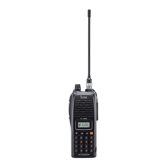
Icom IC-U82 Service Manual
Hide thumbs
Also See for IC-U82:
- Addendum (1 page) ,
- Instruction manual (96 pages) ,
- Specifications (2 pages)
Table of Contents
Advertisement
Quick Links
Download this manual
See also:
Instruction Manual
Advertisement
Table of Contents

Related Manuals for Icom IC-U82


Summary of Contents for Icom IC-U82
- Page 1 ��� ����������� iC-u82...
- Page 2 INTRODUCTION This service manual describes the latest service information for the IC-U82 UHF TRANSCEIVER at the time of publication. MODEL VERSION SYMBOL BATTERY PACK [USA-1] BP-208N [USA-2] BP-222N [USA-3] BP-209N [EUR-1] BP-208N Europe [EUR-2] IC-U82 BP-222N [EUR-3] BP-209N Korea [KOR]...
-
Page 3: Table Of Contents
UT-118 PORT ALLOCATIONS ..................4 - 6 SECTION 5 ADJUSTMENT PROCEDURES 5 - 1 PREPARATION ........................ 5 - 1 5 - 2 IC-U82 ADJUSTMENT ....................5 - 2 5 - 3 UT-118 ADJUSTMENT ....................5 - 4 SECTION 6 PARTS LIST SECTION 7... - Page 4 : 50 Ω (BNC Type) • Antenna impedance • Power supply requirement : Specified Icom's battery packs only (Operating voltage range; 6.0–10.3 V) • Number of memory channels : 207 channels (Including 6 scan edges and 1 call channel) • Scan types : Program/Memory/Skip/Priority/Tone scans •...
- Page 5 SECTION 2 INSIDE VIEWS • MAIN UNIT Top view Bottom view ����� ��������� ����� ��������� ���� ��������� ���� �������� ������������ ������� ��� �� ����� ����� ����������� ����� ��������� ������� �������� �� ��������� ���� ��� ����� ����� ��������� ���� ��������� ������ ������������ ��...
- Page 6 SECTION 3 DISASSEMBLY INSTRUCTIONS 1. Removing the chassis panel 2. Removing the MAIN unit. q Remove the knob A and jack cap B . q Remove the Jack seal F. w Unscrew 1 nut C. w Unsolder 4 points G of the shield cover. e Unscrew 2 screws D (2 ×...
-
Page 7: Circuit Description
SECTION 4 CIRCUIT DESCRIPTION The 1st IF signal from the 1st mixer is passed through the 4-1 RECEIVER CIRCUITS crystal filter (FI1) to suppress unwanted signals, and the 4-1-1 ANTENNA SWITCHING CIRCUIT limiter (D63) and then applied to the 1st IF amplifier (Q14). The antenna switching circuit toggles receive line and transmit line. -
Page 8: Transmitter Circuits
4-1-6 SQUELCH CIRCUIT The signals from the pre-emphasis circuit are passed through the analog switch (IC4, pins 3, 4) and LPF (IC3, Squelch circuit mutes AF output signal when no signals are pins 13, 14). The signals from the LPF are passed through received. -
Page 9: Pll Circuits
The phase detector compares the input signal with the 4-3 PLL CIRCUITS reference frequency, and then outputs the control signal 4-3-1 GENERAL (pulse-type) from pin 5 via the charge pump section. The PLL circuits control the VCO circuit. IC19 is a PLL IC and pulse-type signal is converted into DC voltage at the loop fil- contains prescaler, programmable counter, programmable ter (R445–R448, C472–C474), and then applied to the VCO... -
Page 10: Power Supply Circuits
4-5 POWER SUPPLY CIRCUITS PORT DESCRIPTION 4-5-1 VOLTAGE LINES NUMBER NAME LINE DESCRIPTION NOIS Input port for "NOIS" signal. The voltage from the attached battery pack. ESDA I/O port for EEPROM (IC7). Common 5 V for the CPU (IC8) converted from the Outputs clock signal for EEPROM ESCK CPU5... - Page 11 PORT DESCRIPTION NUMBER NAME PLLSTB Outputs PLL strobe signal. Outputs AF regulator (Q15, Q16) control signal. AFON HIGH : While emitting audio Outputs LPF cut-off frequency control signal to the CTCSS switch (Q38). DUSE LOW : When CTCSS or no signal- ing system is in use.
-
Page 12: Ut-118 Circuit Description
4-7 UT-118 CIRCUIT DESCRIPTION 4-8 UT-118 POWER SUPPLY CIRCUITS 4-7-1 RECEIVER CIRCUIT 4-8-1 VOLTAGE LINES The detected digital signals “FMDET” from the connected LINE DESCRIPTION transceiver via the J301 (pin 22) are amplified at the buffer 5 V from the connected transceiver via the J301 (pin amplifier (IC251, pin 2). -
Page 13: Adjustment Procedures
RF power meter 0.1–20 W/50 Ω • JIG (GND) To [MIC] jack Frequency 68 kΩ counter To [SP] jack 3-conductor 3.5 (d) mm ( 1 /8”) plug (CLONE) IC-U82 • ADJUSTMENT MODE DISPLAY Operating frequency Adjustment item 5 - 1... -
Page 14: Ic-U82 Adjustment
5-2 IC-U82 ADJUSTMENT 5-2-1 KEY OPERATION FOR THE ADJUSTMENT • Rotate [VOL] to adjust the value. • Push [D•CLR] key to store the adjustment value and move to next adjustment item. • Push [ ]/[ ] key to move to next adjustment item without changing the value. - Page 15 ADJUSTMENT ADJUSTMENT CONDITION OPERATION DTCS WAVE • Mode : Wide • Rotate [VOL] to set to square wave form as FORM Connect an oscilloscope and shown below. • the FM deviation meter to the • Push [D•CLR] key. antenna connector. (other than USA) •...
-
Page 16: Ut-118 Adjustment
5-3 UT-118 ADJUSTMENT • CONNECTION (BOTTOM VIEW) Power supply 5.0 V DC / 1 A Power supply 8.0 V DC / 1 A J301, Pin 14 Entering adjustment mode • ADJUSTMENT ADJUSTMENT ADJUSTMENT CONDITION OPERATION ENTERING • Connect the pin 14 of J301 to GND to enter the adjustment mode. ADJUSTMENT MODE CODEC... -
Page 17: Parts List
SECTION 6 PARTS LIST 6-1 IC-U82 [MAIN UNIT] [MAIN UNIT] ORDER ORDER DESCRIPTION DESCRIPTION LOCATION LOCATION [KOR], [EU3], [EX4], [US3] only T 61/41.8 1110003490 S.IC TA31136FN (D) 101.7/33.7 1750000940 S.DIO 1SS400 TE61 Except [EX1], [EX2] T 67.1/40.8 1110006470 S.IC LMV324IPWR 103.7/13.2... - Page 18 [MAIN UNIT] [MAIN UNIT] ORDER ORDER DESCRIPTION DESCRIPTION LOCATION LOCATION S.RES ERJ2GEJ 101 X (100 Ω) R252 7030005310 S.RES ERJ2GEJ 124 X (120 kΩ) 108.8/2.6 7030004980 106.2/6 S.RES ERJ2GEJ 470 X (47 Ω) R257 7030010040 S.RES ERJ2GE-JPW 88.1/16.5 7030004970 106.8/7.9 R258 7030008300 S.RES ERJ2GEJ 184 X (180 kΩ)
- Page 19 [MAIN UNIT] [MAIN UNIT] ORDER ORDER DESCRIPTION DESCRIPTION LOCATION LOCATION 4030017460 S.CER ECJ0EB1E102K 104.7/5.2 R458 7030005050 S.RES ERJ2GEJ 103 X (10 kΩ) 77.3/36.9 4030017460 S.CER ECJ0EB1E102K 109.5/6.6 R459 7030005050 S.RES ERJ2GEJ 103 X (10 kΩ) 74.7/36.5 4030017630 S.CER ECJ0EC1H120J 104.6/5.3 R460 7030008290 S.RES ERJ2GEJ 183 X (18 kΩ)
- Page 20 [MAIN UNIT] [MAIN UNIT] ORDER ORDER DESCRIPTION DESCRIPTION LOCATION LOCATION C477 4030017460 S.CER ECJ0EB1E102K 91.9/30.2 C284 4030007080 S.CER C1608 CH 1H 390J-T 122.2/20.6 C478 4030017460 S.CER ECJ0EB1E102K 97.6/19.1 C287 4030009910 S.CER C1608 CH 1H 040B-T 121.1/14.7 C479 4030016790 S.CER ECJ0EB1C103K 94.9/32 C288 4030017460...
- Page 21 6-2 OPTIONAL UNIT UT-118 [MAIN UNIT] ORDER [MAIN UNIT] DESCRIPTION LOCATION ORDER DESCRIPTION R269 7030005060 S.RES ERJ2GEJ 333 X (33 kΩ) 15.9/8.7 LOCATION R270 7030005240 S.RES ERJ2GEJ 473 X (47 kΩ) 28.5/1.6 1180002390 S.REG S-812C33AMC-C2N-T2 3.4/27.9 7030004980 S.RES ERJ2GEJ 101 X (100 Ω) R308 1.8/16.9 1180002370 S.REG R1111N321B-TR...
- Page 22 SECTION 7 MECHANICAL PARTS AND DISASSEMBLY [CHASSIS PARTS] [ACCESSORIES] REF. REF. NO. ORDER NO. DESCRIPTION QTY. ORDER NO. DESCRIPTION QTY. 6510022460 Connector BNC-R162 EP1 Optional product Antenna FA-B70C EP2 Optional product Battery case BP-208N [USA-1], [EUR-1], [EXP-1] 2510001280 Speaker SDRS-3650P-008A Optional product Battery pack BP-222N [USA-2], [EUR-2], [KOR], [EXP-2] Optional product Battery pack BP-209N [USA-3], [EUR-3], [EXP-4]...
- Page 23 ���� ��� �� ��� ���� ��� ���� ��� ���� ��� ���� ��� ���� ��� ���� ��� ���� ��� ��� �� �� � � �� ��� ��� ��� ��� ���� ��� ���� ��� ���� ��� ���� ��� ���� ��� ���� ��� ����...
- Page 24 SECTION 8 SEMICONDUCTOR INFORMATION •TRANSISTORS AND FET’S •DIODES 2SA1576S 2SC4226 2SA1576A 2SB1132R 2SC4116BL 2SC4617 TLS 1SS400 1SV286 1SV307 1SV308 DA221 TL (Symbol: FS) (Symbol: FA) (Symbol: BAR) (Symbol: LL) (Symbol: BS) (Symbol: A) (Symbol: T7) (Symbol: TX) (Symbol: K) (Symbol: K) 2SC5006-T1 2SC5107-O 2SC5231 C8...
- Page 25 SECTION 9 BOARD LAYOUTS MAIN UNIT • TOP VIEW The combination of this page and next page shows the unit layout in the same configuration as the actual P.C. Board. H100 H105 H110 H115 H120 H125 S801 ENCODER BATT ANTENNA EXT.
- Page 26 • BOTTOM VIEW To Optional unit J301 The combination of this page and previous page shows the unit layout in the same configuration as the actual P.C. Board. H125 H120 H115 H110 H105 H100 MICROPHONE MIC GND 9 - 2...
-
Page 27: Block Diagram
SECTION 10 BLOCK DIAGRAM • MAIN UNIT D64, D71: 1SS400 Q34: 2SK1069 UNLK UNLOCK LVIN ANTENNA Tx: 400.000–479.000 MHz IC16: SN74AHC2C53HDCTR Rx: 353.650–432.650 MHz D1, D72: 1SV307 Tx: 400.000–479.000 MHz X4: CR-783 D3: 1SV308 IC23: Q3: 2SC5107 Q83: 2SC4226 Q2: RD01MUS1 Q1: 2SK3476 D2, D8: MA77 Rx: 400.000–479.000 MHz... - Page 28 SECTION 11 VOLTAGE DIAGRAM PLLSW PLLSW CPU5 CPU5 PSVCO CTCSS CTCSS • MAIN UNIT SW5V SW5V LIGHT ON: 3.50V OFF: 4.40V SW5V CPU5 SW5V R369 LNJ310M6URA C412 CTCSS CTCSS C413 0.01 SW5V SW5V 0.001 LNJ310M6URA 2SA1576A R500 R377 330k 180k IC23 R491 R195...
- Page 29 PLLSW PSVCO PSVCO R160 PSVCO 4.80V SW5V SW5V SW5V C443 C441 C535 R515 XP4601 R433 R337 C518 R422 C489 0.001 470p R441 1.5M 3.40V C288 C204 0.001 0.001 3.20V 2.2M 3.70V 0.001 EXCCL3225U1 C459 0.001 0.001 IC19 C449 0.82µH C429 C477 C463 0.001...
-
Page 30: Disassembly Information
SECTION 12 BC-146 BATTERY CHARGER 12-1 PARTS LIST 12-2 DISASSEMBLY INFORMATION [CHARGE UNIT] REF. NO. ODER NO. DESCRIPTION QTY. 7010007550 RESISTOR ERG3SJ680H 7010007100 RESISTOR PSD1/4V 1 kΩ 6510021470 CONNECTOR HEC0470-01-230 5040001390 LED TLG124A 0910053820 PCB B 5650 8930051340 2338 TERMINAL 8930051340 2338 TERMINAL [CHASSIS UNIT] REF. -
Page 31: Voltage Diagram
12-3 VOLTAGE DIAGRAM C : 13.8V C : 7.2V N : 13.8V N : 13.8V R1 68 TLG124A HEC0470-01-230 C : 9.2V N : 13.8V 12-4 BOARD LAYOUT 12 - 2... -
Page 32: Ut-118 Digital Unit (Optional Unit)
SECTION 13 UT-118 DIGITAL UNIT (OPTIONAL UNIT) 13-1 UT-118 BOARD LAYOUT • TOP VIEW • BOTTOM VIEW J301 PTTIN PTTOUT MICOUT VCC_8V MICIN — 232TX — BUSY 232RX — RXMUTE SICO FMDET OPT1 AFOUT OPT2 REFMOD OPT3 — OPV3 OPSO OPV2 OPV1 OPSCK... -
Page 33: Ut-118 Semiconducter Information
13-3 UT-118 BLOCK DIAGRAM 13-2 UT-118 SEMICONDUCTOR INFORMATION • TRANSISTORS AND FET’S FOR FM_TRANCEVER OPTION CONNECTOR 2SA1586 GR DTC144EUA T106 XP4312 (Symbol: SG) (Symbol: 26_) (Symbol: 7T) FLASH WRITER F_RXD Explanatory notes Q305 XP4312 VOLTAGE LINE Q306 XP4312 TX LINE LEVEL FOR FM_TRANCEVER CPU TXD_2... -
Page 34: Ut-118 Voltage Diagram
13-4 UT-118 VOLTAGE DIAGRAM 3.3V L201 1µ 3.3V 3.3V 3.3V APWR APWR 3.3V IC203 X201 S-80928CNMC CR-760 4.0-8.5V 3.2V S-812C33AMC-C2N-T2 R1111N321B (9.8304 MHz) PSAVE ON: L(0.0V) VOUT VOUT PSAVE OFF: H(3.3V) R209 R400 100k PSAVE ON: L(0.0V) AEPR Q401 PSAVE OFF: H(3.3V) Q400 R401 DTC144EU... - Page 35 E-mail : info@icomcanada.com Unit 9, Sea St., Herne Bay, Kent, CT6 8LD, U.K. Phone : +44 (01227) 741741 Fax : +44 (01227) 741742 Icom (Australia) Pty. Ltd. : http://www.icomuk.co.uk E-mail : info@icomuk.co.uk A.B.N. 88 006 092 575 290-294 Albert Street, Brunswick, Victoria, 3056, Australia Icom France S.a...
Need help?
Do you have a question about the IC-U82 and is the answer not in the manual?
Questions and answers