Sony DSC-T10 Service Manual
Digital still camera
Hide thumbs
Also See for DSC-T10:
- Handbook (119 pages) ,
- Handbook (116 pages) ,
- Instruction manual (32 pages)
Table of Contents
Advertisement
Quick Links
Download this manual
See also:
Handbook
SERVICE MANUAL
Ver 1.1 2006.09
Revision History
Revision History
How to use
How to use
Acrobat Reader
Acrobat Reader
Internal memory
Internal memory
ON BOARD
ON BOARD
Link
Link
SERVICE NOTE
SCHEMATIC DIAGRAMS
The components identified by
mark 0 or dotted line with
mark 0 are critical for safety.
Replace only with part num-
ber specified.
DSC-T10_L3
9-852-129-11
PRINTED WIRING BOARDS
Les composants identifiés par une
marque 0 sont critiques pour la
sécurité.
Ne les remplacer que par une pièce
portant le numéro spécifié.
Sony EMCS Co.
DSC-T10
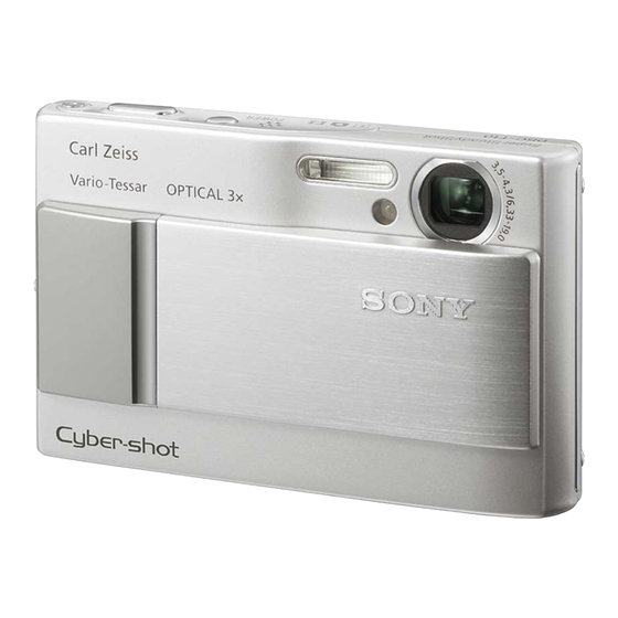
Photo: Silver
DIGITAL STILL CAMERA
LEVEL
US Model
Canadian Model
AEP Model
UK Model
E Model
Australian Model
Hong Kong Model
Chinese Model
Korea Model
Argentine Model
Brazilian Model
Japanese Model
Tourist Model
REPAIR PARTS LIST
Published by Kohda TEC
3
2006I0500-1
© 2006.9
Advertisement
Table of Contents

Related Manuals for Sony DSC-T10


Summary of Contents for Sony DSC-T10
- Page 1 0 are critical for safety. sécurité. Replace only with part num- Ne les remplacer que par une pièce ber specified. portant le numéro spécifié. DIGITAL STILL CAMERA 2006I0500-1 DSC-T10_L3 © 2006.9 Sony EMCS Co. 9-852-129-11 Published by Kohda TEC...
- Page 2 CRITIQUES POUR LA SÉCURITÉ DE FONCTIONNEMENT. NE COMPONENTS WITH SONY PARTS WHOSE PART NUMBERS REMPLACER CES COMPOSANTS QUE PAR DES PIÈSES SONY APPEAR AS SHOWN IN THIS MANUAL OR IN SUPPLEMENTS DONT LES NUMÉROS SONT DONNÉS DANS CE MANUEL OU PUBLISHED BY SONY.
-
Page 3: Table Of Contents
TABLE OF CONTENTS Section Title Page SERVICE NOTE 1-3. Method for Copying or Erasing the Data in Internal Memory (Internal Memory/Music) ································· 1-2 PRINTED WIRING BOARDS AND SCHEMATIC DIAGRAMS 4-2. Schematic Diagrams ························································ 4-3 4-3. Printed Wiring Boards ··················································· 4-15 4-4. -
Page 4: Service Note
1. SERVICE NOTE 1-3. METHOD FOR COPYING OR ERASING THE DATA IN INTERNAL MEMORY (INTERNAL MEMORY/MUSIC) The data can be copied/erased by the operations on the Setup screen. (When erasing the data, execute formatting the internal memory.) Note 1: When replacing the SY-163 board, erase the data in internal memory of the board before replacement. Note 2: When replacing the SY-163 board or the IC401 on the SY-163 board, execute formatting and initialize the internal memory after replacement. -
Page 5: Schematic Diagrams
4-2. SCHEMATIC DIAGRAMS Link Link SY-163 BOARD (1/6) SY-163 BOARD (4/6) (SDRAM, SUPER AND) (CCD SIGNAL PROCESS) SY-163 BOARD (2/6) SY-163 BOARD (5/6) (AUDIO, VIDEO) (LENS DRIVE, OIS DRIVE) SY-163 BOARD (3/6) (CAMERA DSP) SY-163 BOARD (6/6) (DC/DC CONVERTER) COMMON NOTE FOR SCHEMATIC DIAGRAMS DSC-T10_L3... -
Page 6: Printed Wiring Boards And Schematic Diagrams
4-2. SCHEMATIC DIAGRAMS 4-2. SCHEMATIC DIAGRAMS 4. PRINTED WIRING BOARDS AND SCHEMATIC DIAGRAMS 4-2. SCHEMATIC DIAGRAMS THIS NOTE IS COMMON FOR SCHEMATIC DIAGRAMS (In addition to this, the necessary note is printed in each block) (For schematic diagrams) 1. Connection •... - Page 7 SY-163 BOARD (1/6) : Voltage measurement of the CSP ICs and the Transistors with mark, are not possible. CCD SIGNAL PROCESS XX MARK:NO MOUNT NO MARK:REC/PB MODE R:REC MODE P:PB MODE R119 CA_AD0 CA_AD0 CA_AD1 CA_AD1 CA_AD2 CA_AD2 CA_AD3 CA_AD3 CA_AD4 CA_AD4 CA_AD5...
- Page 8 SY-163 BOARD (2/6) : Voltage measurement of the CSP ICs and the Transistors with mark, are LENS DRIVE, OIS DRIVE not possible. XX MARK:NO MOUNT NO MARK:REC/PB MODE R559 C516 C539 IC504 C549 1.5V REG VCONT C533 0.1u IC504 TK63115BCB-G R536 R545 100k...
- Page 9 SY-163 BOARD (3/6) : Voltage measurement of the CSP ICs CA_AD0 USB_VBUS (5/6) CPU_D00 CA_AD0 USB_VBUS CPU_D00 and the Transistors with mark, are (6/6) CA_AD1 CPU_D01 not possible. CA_AD1 CPU_D01 CAMERA DSP CA_AD2 CPU_D02 CA_AD2 MS_PWR_ON CPU_D02 MS_PWR_ON Q305 CA_AD3 CPU_D03 XX MARK:NO MOUNT CA_AD3...
- Page 10 SY-163 BOARD (4/6) : Voltage measurement of the CSP ICs and the Transistors with mark, are not possible. SDRAM, SUPER AND XX MARK:NO MOUNT C404 C408 C405 C406 0.1u 0.1u 0.1u 0.1u (1/6) XIC_301_RST_OUT XIC_301_RST_OUT (2/6) R401 (3/6) DSP_AQ00 C403 XCPU_CS4 DSP_AQ00 XCPU_CS4...
- Page 11 SY-163 BOARD (5/6) BATT/XEXT AUDIO, VIDEO : Voltage measurement of the CSP ICs ACV_UNREG and the Transistors with mark, are CHARGE_V (6/6) XX MARK:NO MOUNT not possible. CN711 ACV_GND (6/6) ACV_GND ACV_GND MS_VCC ACV_GND M_5V (6/6) REG_GND ACV_GND A_3.2V REG_GND (ACV_GND) (SP_GND) XPOWER_ON...
- Page 12 • Refer to page 4-3 for mark 0. SY-163 BOARD (6/6) : Voltage measurement of the CSP ICs and the Transistors with mark, are not possible. DC/DC CONVERTER XX MARK:NO MOUNT NO MARK:REC/PB MODE R:REC MODE P:PB MODE F001 (2A/32V) ACV_UNREG ST_UNREG (3/6)
-
Page 13: Printed Wiring Boards
4-3. PRINTED WIRING BOARDS Link Link SY-163 BOARD (SIDE A) SY-163 BOARD (SIDE B) COMMON NOTE FOR PRINTED WIRING BOARDS MOUNTED PARTS LOCATION DSC-T10_L3... - Page 14 4-3. PRINTED WIRING BOARDS 4-3. PRINTED WIRING BOARDS 4-3. PRINTED WIRING BOARDS THIS NOTE IS COMMON FOR PRINTED WIRING BOARDS • : Uses unleaded solder. • Chip parts. • : Circuit board Transistor Diode : Flexible board Pattern from the side which enables seeing. : pattern of the rear side (The other layers’...
- Page 15 SY-163 (8 layers) : Uses unleaded solder. SY-163 BOARD (SIDE A) R742 CN703 3.2V R741 C202 IC201 L003 C013 L009 A7 B7 C7 D7 E7 F7 G7 A6 B6 C6 D6 E6 F6 G6 C012 A5 B5 C5 D5 E5 F5 G5 C011 R204 A4 B4 C4 D4 E4 F4 G4...
- Page 16 SY-163 (8 layers) : Uses unleaded solder. SY-163 BOARD (SIDE B) Q008 R050 D009 D008 D002 C065 C063 F001 R048 Q001 R049 D007 R042 Q002 L030 F002 F003 L002 C043 L007 D003 BL_H R002 C017 (16V) C034 1.2V CAM_2.9V D_3.2V R073 L102 L104...
-
Page 17: Mounted Parts Location
4-3. PRINTED WIRING BOARDS 4-3. PRINTED WIRING BOARDS 4-4. MOUNTED PARTS LOCATION no mark : side A * mark : side B SY-163 BOARD * C001 C319 C729 L702 R351 X001 C002 C320 C730 L703 R352 X302 C003 C321 C731 R356 C004 C322... -
Page 18: Repair Parts List
5. REPAIR PARTS LIST NOTE: • -XX, -X mean standardized parts, so they may have some differences from When indicating parts by reference number, the original one. please include the board name. • Items marked “*” are not stocked since they are seldom required for routine The components identified by mark 0 or service. -
Page 19: Electrical Parts List
SY-163 5-2. ELECTRICAL PARTS LIST Ref. No. Part No. Description Ref. No. Part No. Description A-1202-375-A SY-163 BOARD, COMPLETE (SERVICE) (GP1) C114 1-100-539-91 TANTAL. CHIP 47uF 6.3V A-1202-376-A SY-163 BOARD, COMPLETE (SERVICE) (GP2) C115 1-100-539-91 TANTAL. CHIP 47uF 6.3V A-1202-377-A SY-163 BOARD, COMPLETE (SERVICE) (GP3) A-1202-378-A SY-163 BOARD, COMPLETE (SERVICE) (GP4) C116 1-164-937-11 CERAMIC CHIP... - Page 20 SY-163 Ref. No. Part No. Description Ref. No. Part No. Description C404 1-100-504-91 CERAMIC CHIP 0.1uF 6.3V C706 1-100-507-91 CERAMIC CHIP 4.7uF 6.3V C719 1-125-777-11 CERAMIC CHIP 0.1uF C405 1-100-504-91 CERAMIC CHIP 0.1uF 6.3V C724 1-100-735-91 CERAMIC CHIP 10uF C406 1-100-504-91 CERAMIC CHIP 0.1uF 6.3V...
- Page 21 SY-163 Ref. No. Part No. Description Ref. No. Part No. Description FB309 1-469-581-21 INDUCTOR, FERRITE BEAD (1005) R002 1-218-985-11 RES-CHIP 470K 1/16W FB310 1-469-581-21 INDUCTOR, FERRITE BEAD (1005) R003 1-218-989-11 RES-CHIP 1/16W FB311 1-469-580-11 INDUCTOR, FERRITE BEAD (1005) R004 1-240-724-91 METAL CHIP 330K 1/20W FB701...
- Page 22 SY-163 Ref. No. Part No. Description Ref. No. Part No. Description R314 1-218-973-11 RES-CHIP 1/16W R550 1-240-718-91 METAL CHIP 100K 1/20W R551 1-218-977-11 RES-CHIP 100K 1/16W R315 1-218-942-11 RES-CHIP 1/16W R555 1-240-711-91 METAL CHIP 1/20W R321 1-218-973-11 RES-CHIP 1/16W R556 1-240-711-91 METAL CHIP 1/20W R325...
- Page 23 Brazilian Model SUPPLEMENT-1 Japanese Model Tourist Model File this supplement with the service manual. (DI06-069) • Addition of Brazilian Model The differences with other area models are only accessories. 2006I0500-1 DSC-T10_L3 © 2006.9 Sony EMCS Co. 9-852-129-83 Published by Kohda TEC...
- Page 24 [Description of main button functions on toolbar of the Adobe Acrobat Reader Ver5.0 (for Windows)] Toolbar Printing a text Reversing the screens displayed once • To reverse the previous screens (operation) one by one, click 1. Click the Print button 2.
-
Page 25: Revision History
Reverse 985212912.pdf Revision History S.M. Rev. Ver. Date History Contents issued 2006.07 Official Release — — 2006.09 Supplement-1 • Addition of Brazilian Model (S1 DI06-069) DSC-T10_L3...
Need help?
Do you have a question about the DSC-T10 and is the answer not in the manual?
Questions and answers