Advertisement
Table of Contents
- 1 Table of Contents
- 2 Specifications
- 3 Pcbs Location
- 4 Software Check and Upgrade
- 5 Safety Instruction
- 6 Mechanical and Dismantling Instructions
- 7 Troubleshooting Chart
- 8 No Display on VFD, and Buttons Do Not Work
- 9 No Audio Output
- 10 Remote Control Does Not Work
- 11 Can’t Read Disc or Can’t Open the Disk Door
- 12 No VFD Display
- 13 Overall Block Diagram
- 14 Circuit Diagrams
- 15 PCB Views
- 16 Exploded View Diagram
- Download this manual
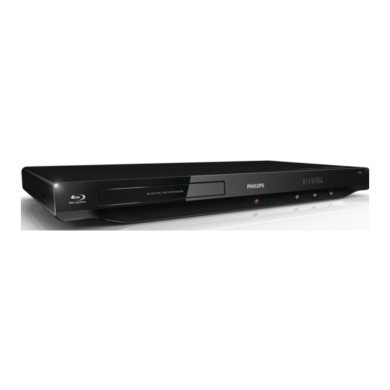
Blu-ray Disc Player
TABLE OF CONTENTS
Technical Specification, PCBs Location....................... 1
Safety Instruction ...................................................... 2
Instruction for Use...................................................... 3
Mechanical And Dismantling Instructions...................... 4
Service Modes, Troubleshooting.................................. 5
Overall Block Diagram, Wiring Diagram......................... 6
Electrical Diagram...................................................... 7
Exploded View Diagram & Service Part List....................8
Revision List............................................................. 9
©
Copyright 2011 Philips Consumer Electronics B.V. Eindhoven, The Netherlands
All rights reserved. No part of this publication may be reproduced, stored in a retrieval system or
transmitted, in any form or by any means, electronic, mechanical, photocopying, or otherwise without
the prior permission of Philips.
Published by CY_SL1108 BG AVM Printed in The Netherlands
Version 1.1
Version 0.0
BDP3200(X)
Chapter
LASER PRODUCT
Subject to modification
/51/55/77/78
CLASS 1
314178535911
Advertisement
Table of Contents


Need help?
Do you have a question about the BDP3200/51 and is the answer not in the manual?
Questions and answers