Table of Contents
Advertisement
Please refer to the original service manual for:
CD Mechanism Unit Order No. PSG1303059AE
Speaker system SB-MAX5000PN/PS, Order No. PSG1603009CE
TABLE OF CONTENTS
1 Safety Precautions----------------------------------------------- 3
1.1. General Guidelines---------------------------------------- 3
1.2. Before Repair and Adjustment ------------------------- 4
1.3. Protection Circuitry ---------------------------------------- 4
1.4. Safety Parts Information -------------------------------- 5
2 Warning -------------------------------------------------------------- 6
to Electrostatically Sensitive (ES) Devices---------- 6
2.2. Precaution of Laser Diode------------------------------- 6
(PbF)---------------------------------------------------------- 7
2.4. Handling Precautions for Traverse Ass'y------------ 7
prevention --------------------------------------------------- 8
3 Service Navigation ----------------------------------------------- 9
PAGE
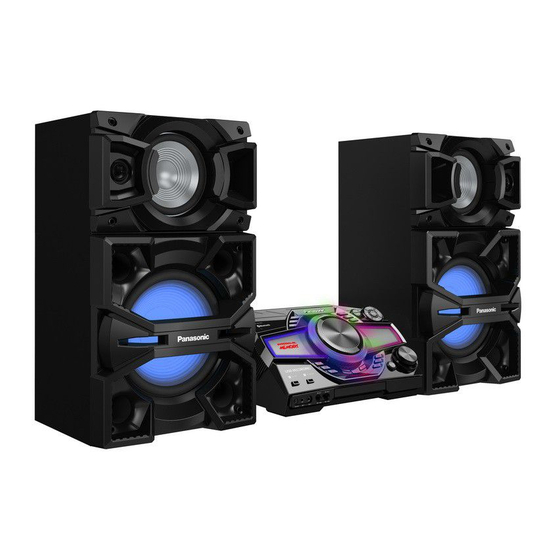
SA-MAX5000PN
Model No.
SA-MAX5000PS
Product Color: (K)...Black Type
3.1. Service Information ----------------------------------------9
3.2. Software Update Procedure-----------------------------9
4 Specifications ---------------------------------------------------- 10
5 Location of Controls and Components------------------ 11
5.1. Remote Control Key Button Operation ------------- 11
5.2. Main Unit Key Button Operation---------------------- 12
6 Service Mode ----------------------------------------------------- 13
6.1. Cold-Start -------------------------------------------------- 13
6.2. Sales Demonstration Lock Function ---------------- 13
6.3. Doctor Mode Table--------------------------------------- 14
6.4. Self-Diagnostic Mode ----------------------------------- 16
6.5. Self-Diagnostic Error Code Table -------------------- 16
7 Troubleshooting Guide --------------------------------------- 18
7.1. No Power or No Display ------------------------------- 18
7.2. Bluetooth® Pairing Failure----------------------------- 18
© Panasonic Corporation 2016. All rights reserved.
Unauthorized copying and distribution is a violation
of law.
PSG1603007CE
CD Stereo System
PAGE
Advertisement
Table of Contents

Related Manuals for Panasonic SA-MAX5000PN


Summary of Contents for Panasonic SA-MAX5000PN
-
Page 1: Table Of Contents
7 Troubleshooting Guide --------------------------------------- 18 prevention --------------------------------------------------- 8 7.1. No Power or No Display ------------------------------- 18 3 Service Navigation ----------------------------------------------- 9 7.2. Bluetooth® Pairing Failure----------------------------- 18 © Panasonic Corporation 2016. All rights reserved. Unauthorized copying and distribution is a violation of law. - Page 2 7.3. No Key Function------------------------------------------ 18 7.4. No Remote Control Function -------------------------- 18 7.5. No NFC ----------------------------------------------------- 19 7.6. USB Device Cannot Detect---------------------------- 19 7.7. No Output Sound----------------------------------------- 20 7.8. Check Point------------------------------------------------ 21 8 Disassembly and Assembly Instructions --------------- 22 8.1. Type of Screws ------------------------------------------- 22 8.2.
-
Page 3: Safety Precautions
1 Safety Precautions 1.1. General Guidelines 1. IMPORTANT SAFETY NOTICE There are special components used in this equipment which are important for safety. These parts are marked by in the Schematic Diagrams, Circuit Board Layout, Exploded Views and Replacement Parts List. It is essential that these critical parts should be replaced with manufacturer’s specified parts to prevent X-RADIATION, shock, fire, or other hazards. -
Page 4: Before Repair And Adjustment
1.2. Before Repair and Adjustment Disconnect AC power to discharge AC capacitor (in SMPS P.C.B.) as indicate below diagram through a 10 , 10 W resistor to ground. Figure 1-2 Caution: DO NOT SHORT-CIRCUIT DIRECTLY (with a screwdriver blade, for instance), as this may destroy solid state devices. After repairs are completed, restore power gradually using a variac, to avoid overcurrent. -
Page 5: Safety Parts Information
1.4. Safety Parts Information Safety Parts List: There are special components used in this equipment which are important for safety. These parts are marked by in the Schematic Diagrams, Exploded View & Replacement Parts List. It is essential that these critical parts should be replaced with manufacturer’s specified parts to prevent shock, fire or other hazards. -
Page 6: Warning
2 Warning 2.1. Prevention of Electrostatic Discharge (ESD) to Electrostatically Sensi- tive (ES) Devices Some semiconductor (solid state) devices can be damaged easily by static electricity. Such components commonly are called Elec- trostatically Sensitive (ES) Devices. The following techniques should be used to help reduce the incidence of component damage caused by electrostatic discharge (ESD). -
Page 7: General Description About Lead Free Solder (Pbf)
Figure 2-1 2.3. General description about Lead Free Solder (PbF) The lead free solder has been used in the mounting process of all electrical components on the printed circuit boards used for this equipment in considering the globally environmental conservation. The normal solder is the alloy of tin (Sn) and lead (Pb). -
Page 8: Grounding For Electrostatic Breakdown Prevention
ble cable, cut off the antistatic FFC. Figure 2-2 2.5. Grounding for electrostatic breakdown prevention • As for parts that use optical pick-up (laser diode), the optical pick-up is destroyed by the static electricity of the working environ- ment. Repair in the working environment that is grounded. 2.5.1. -
Page 9: Service Navigation
3 Service Navigation 3.1. Service Information This service manual contains technical information which will allow service personnel’s to understand and service this model. Please place orders using the parts list and not the drawing reference numbers. If the circuit is changed or modified, this information will be followed by supplement service manual to be filed with original service manual. -
Page 10: Specifications
Class Class 2 Supported profiles A2DP, AVRCP, SPP, OPP, FTP System: SC-MAX5000PN Operating frequency 2.4 GHz band FH-SS Main Unit: SA-MAX5000PN Operation distance 10 m line of sight Speaker System: SB-MAX5000PN Internal memory section System: SC-MAX5000PS Memory... -
Page 11: Location Of Controls And Components
5 Location of Controls and Components 5.1. Remote Control Key Button Operation... -
Page 12: Main Unit Key Button Operation
5.2. Main Unit Key Button Operation Top View Front View... -
Page 13: Service Mode
6 Service Mode 6.1. Cold-Start Item Key Operation FL Display Mode Name Description Front Key Cold Start To carry out cold-start or initialize 1. Unplug AC power cord. to shipping mode 2. Press & hold [POWER] button. 3. Plug in AC power cord while [POWER] button being pressed. -
Page 14: Doctor Mode Table
6.3. Doctor Mode Table 6.3.1. Doctor Mode Table 1 Item Key Operation FL Display Mode Name Description Front Key Doctor Mode 1. Press [ ] button on main unit follow by [4] and [7] on remote control. 2. To exit, press [ /I] on main unit or remote control EEPROM Displaying of... - Page 15 6.3.2. Doctor Mode Table 2 Item Key Operation FL Display Mode Name Description Front Key Volume Setting To check the volume setting of the In Doctor Mode: Check main unit. 1. Press [7], [8], [9] button on the remote control. Press [7]: VOL50 Volume Press [8]: VOL35...
-
Page 16: Self-Diagnostic Mode
6.4. Self-Diagnostic Mode Item Key Operation FL Display Mode Name Description Front Key Self Diagnostic c i t Mode (Ensure no disc is inserted). Step 2: Press & hold [ ] button follow by [ ] on main unit for 2 seconds. Error Code System will perform a check on c i t... - Page 17 6.5.2. CD Mechanism Error Code Table Item Key Operation Solution FL Display (PCB exchange repair) Mode Name Description Front Key Error Code Diagnosis Contents: Press [ ] on main unit Check following: CD H15 CD Open Abnormal for next error. 1.
-
Page 18: Troubleshooting Guide
7 Troubleshooting Guide 7.1. No Power or No Display Caution: 1. AC Cord Plug-out Check Secondary Cap. (C1601) Press Power Button Check Primary E-Cap (C1403) 2. Check Fuse(F1001) = 0 ohm No Display on or Secondary Diode (D1601) of Unit or Remote Control Measured 200V or more 3. -
Page 19: No Nfc
7.5. No NFC Press [SELECTOR and choose Check and Do Setting of NFC. Press Power Button Set ON when Tap the Set will Display No Problem BLUETOOTH] OFF the Set and Tap the Phone of Unit or Remote Control Phone on NFC Logo "BLUETOOTH"... -
Page 20: No Output Sound
7.7. No Output Sound CD Play Press Power Button Press Play No Problem Output Sound of Unit or Remote Control CD Mode FL Display "Track & Count" Found to Turn ON the Unit Check IC4202, Check CD Mechanism & FFC connection IC4005 Main P.C.B USB Play Insert USB Thumdrive... -
Page 21: Check Point
7.8. Check Point 7.8.1. SMPS P.C.B. 7.8.2. Main P.C.B. -
Page 22: Disassembly And Assembly Instructions
8 Disassembly and Assembly Instructions • This section describes the disassembly and/or assembly procedures for all major printed circuit boards & main compo- nents for the unit. (You may refer to the section of “Main components and P.C.B Locations” as described in this service manual) •... -
Page 23: Disassembly Flow Chart
8.2. Disassembly Flow Chart Top Cabinet Front Panel Unit Panel P.C.B. SMPS P.C.B. NFC P.C.B. Main P.C.B. USB P.C.B. CD Mechanism Unit Mic P.C.B. CD Interface P.C.B. 8.3. Main Components and P.C.B. Locations... -
Page 24: Disassembly Of Top Cabinet
8.4. Disassembly of Top Cabinet 8.5. Disassembly of Front Panel Unit Step 1 Remove 5 screws. • Refer to “Disassembly of Top Cabinet Assembly Unit”. Step 1 Detach 12P Cable at connector (P9001) on Main P.C.B.. Step 2 Detach 9P Cable at connector (P1803) on Main P.C.B.. Step 3 Detach 30P FFC at connector (P1802) on Main P.C.B.. -
Page 25: Disassembly Of Panel P.c.b
8.6. Disassembly of Panel P.C.B. Step 4 Release catches. Step 5 Remove Panel P.C.B.. • Refer to “Disassembly of Top Cabinet Assembly Unit”. • Refer to “Disassembly of Front Panel Unit”. Step 1 Remove DJ Table. Step 2 Remove Volume Knob. Step 3 Remove 15 screws. -
Page 26: Disassembly Nfc P.c.b
8.7. Disassembly NFC P.C.B. 8.9. Disassembly of Mic P.C.B. • Refer to “Disassembly of Top Cabinet Assembly Unit”. • Refer to “Disassembly of Top Cabinet Assembly Unit”. • Refer to “Disassembly of Front Panel Unit”. • Refer to “Disassembly of Front Panel Unit”. Step 1 Remove Mic Knob. -
Page 27: Disassembly Of Smps P.c.b
8.10. Disassembly of SMPS P.C.B. 8.11. Disassembly of Main P.C.B. • Refer to “Disassembly of Top Cabinet Assembly Unit”. • Refer to “Disassembly of Top Cabinet Assembly Unit”. • Refer to “Disassembly of Front Panel Unit”. • Refer to “Disassembly of Front Panel Unit”. Step 1 Remove screw. -
Page 28: Disassembly Of Cd Mechanism Unit
Step 3 Detach 13P Cable at connector (CN1851) on SMPS 8.13. Disassembly of CD Interface P.C.B.. P.C.B. Step 4 Detach 2P Cable at connector (CN2105) on Main P.C.B.. • Refer to “Disassembly of Top Cabinet”. Step 5 Detach 2P Cable at connector (CN2104) on Main •... -
Page 29: Service Position
9 Service Position Note: For description of the disassembly procedures, refer Section 8 of the Service Manual. 9.1. Checking of Panel P.C.B. 9.2. Checking of SMPS P.C.B. Step 1 Remove Top Cabinet. Step 1 Remove Top Cabinet. Step 2 Remove Front Panel Unit. Step 2 Remove SMPS P.C.B.. -
Page 30: Checking Of Main P.c.b
9.3. Checking of Main P.C.B. Step 1 Remove Top Cabinet. Step 2 Remove Main P.C.B.. Step 3 Place Main P.C.B. on the insulated material as shown. Step 4 Attach 13P Cable at connector (CN1851) on SMPS P.C.B.. Step 5 Attach 2P Cable at connector (CN2105) on Main P.C.B.. Step 6 Attach 2P Cable at connector (CN2104) on Main P.C.B.. -
Page 31: Block Diagram
(PLAY) BT UART RTS P7701* P1804 UART0 RTS P9001 CN6002 D+ A D+ A USB0_DP 98 3 USB A D+ BT LDO ON P7701* P1804 NOTE: “ * ” REF IS FOR INDICATION ONLY SA-MAX5000PN/PS SYSTEM CONTROL (1/4) BLOCK DIAGRAM... - Page 32 MSDO 24 CIRCUIT P1802 P6200 FL DATA FL DATA MSCLK 23 +3.3V IC2001 4GB NAND FLASH MEMORY DAT1 SD DAT1 DAT3 SD DAT3 DAT3 IR6301 REMOTE SENSOR P1802 P6200 REM IN REM IN +3.3V SA-MAX5000PN/PS SYSTEM CONTROL (2/4) BLOCK DIAGRAM...
- Page 33 LED DRIVE X1 30 LED DRIVE +3.3V QR8503 X2 OUT LED DRIVE X2 31 SB-MAX5000 P1502 P1502 QR8505 Q8513 P1502 TO SYSTEM CONTROL P1502 Y1 OUT LED DRIVE SWITCH Y1 26 +5.4V BLOCK (4/4) SA-MAX5000PN/PS SYSTEM CONTROL (3/4) BLOCK DIAGRAM...
- Page 34 POWER UP KPY11 2 POWER UP USB A PCONT USB A PCONT PX4 23 USB B PCONT KPY5 USB B PCONT PCONT2 KPX7 PCONT2 FROM/TO PCONT3 POWER SUPPLY TO SYSTEM CONTROL BLOCK (3/4) NRST NRST SA-MAX5000PN/PS SYSTEM CONTROL (4/4) BLOCK DIAGRAM...
-
Page 35: Audio
SYSTEM CONTROL TUN WCK TUN WCK DFS 14 TUN WCK G TUN BCK TUN BCK TUN BCK DCLK 17 I2C SCL I2C SCL I2C SCL FROM/TO SCLK SYSTEM CONTROL I2C SDA I2C SDA SDIO I2C SDA SA-MAX5000PN/PS AUDIO (1/2) BLOCK DIAGRAM... - Page 36 INPUT A BST A INPUT B OUT A OUT A OUT B BST B TO AUDIO BLOCK (1/2) BST C JK3500 /RST OUT C SUBWOOFER JK3500 LEFT OUT D OUT D /OTW /FAULT BST D SA-MAX5000PN/PS AUDIO (2/2) BLOCK DIAGRAM...
-
Page 37: Power Supply
VS 15 Q1502 SWITCH VGL 11 CS1 7 CS2 8 D1502 VB 14 POWER MODE D1503 QR1720 VC2 10 SWITCH FEEDBACK CIRCUIT IC1501 SWITCHING POWER SUPPLY IC1701 SHUNT REGULATOR D1705 Q1505 +40V D1703 PRIMARY SECONDARY SA-MAX5000PN/PS POWER SUPPLY (1/3) BLOCK DIAGRAM... - Page 38 POWER UP SYNC CN1851 CN2103 SYNC PW SW3R3V SYNC 3 VIN VOUT 2 +3.3V TEMP DET CN1851 CN2103 TEMP DET TEMP DET PW SW3R3V PW SW5R4V +5.4V PW SW5R4V TO POWER SUPPLY BLOCK (2/3) SA-MAX5000PN/PS POWER SUPPLY (2/3) BLOCK DIAGRAM...
- Page 39 SYSTEM CONTROL USB B SW5R1V USB_B_SW5R1V P9001 CN6002 USB5V USB OVC 3 FLAG VO 1 USB B PCONT 4 EN IC9003 5 VIN HIGH SIDE SWITCH NOTE: “ * ” REF IS FOR INDICATION ONLY SA-MAX5000PN/PS POWER SUPPLY (3/3) BLOCK DIAGRAM...
-
Page 40: Wiring Connection Diagram
TO FAN UNIT (RIGHT) CN7002 P1804 P1802 P1803 P9001 P5002 CN7001 TO OPTICAL PICKUP UNIT (CD MECHANISM UNIT) TO CD LOADING P.C.B. (CD MECHANISM UNIT) P7701 NFC P.C.B. P6200 PANEL P.C.B. CN1401 MIC P.C.B. CN6002 USB P.C.B. SA-MAX5000PN/PS WIRING CONNECTION DIAGRAM... -
Page 41: Schematic Diagram
12 Schematic Diagram 12.1. Schematic Diagram Notes • Voltage and signal line : +B signal line • This schematic diagram may be modified at any time : CD signal line with the development of new technology. : Mic/Aux/Tuner signal line Notes: : Audio signal line : USB signal line... -
Page 43: Main (Damp) Circuit (1/2)
IO: MAIN (IO EXPANSION): SCHEMATIC DIAGRAM - 8 GVDD_CD BST_D C3123 MI: MAIN (MICON): SCHEMATIC DIAGRAM - 9 ~ 10 C3106 0.033 US: MAIN (USB): SCHEMATIC DIAGRAM - 10 TO MAIN (DAMP) CIRCUIT (2/2) R3111 R3110 SA-MAX5000PN/PS MAIN (DAMP) CIRCUIT... -
Page 44: Main (Damp) Circuit (2/2)
INPUT_D PVDD_CD 0.01 /FAULT PVDD_CD R3528 R3526 /OTW OUT_D 100K R3115 /CLIP OUT_D R3309 C3326 L3301 R3663 0.033 G0C100M00013 R3311 BST_C R3662 TO MAIN (DAMP) GVDD_CD BST_D CIRCUIT (1/2) C3327 C3307 0.033 R3661 DAMP_GND R3317 R3316 SA-MAX5000PN/PS MAIN (DAMP) CIRCUIT... -
Page 45: Main (Fan Led) Circuit
R2149 R2148 B1ABCF000231 B1ABCF000231 A+IN B-IN 270K Q2110 6.8K C2129 FAN CONTROL FAN CONTROL R2155 B1ABCF000231 R2119 B+IN C2101 R2103 FAN CONTROL R2154 D2103 C2108 DA2J10100L C2130 R2152 R2150 R2151 C2131 FAN_OUT DC_DET_AMP MGND PW_SW15R0V SA-MAX5000PN/PS MAIN (FAN LED) CIRCUIT... -
Page 46: Main (Cd Motor Driver) Circuit
TU: MAIN (TUNER AUX): SCHEMATIC DIAGRAM - 7 IO: MAIN (IO EXPANSION): SCHEMATIC DIAGRAM - 8 MI: MAIN (MICON): SCHEMATIC DIAGRAM - 9 ~ 10 ZJ5001 US: MAIN (USB): SCHEMATIC DIAGRAM - 10 K9ZZ00001279 SA-MAX5000PN/PS MAIN (CD MOTOR DRIVER) CIRCUIT... -
Page 47: Main (Vreg Fan) Circuit (1/2)
IO: MAIN (IO EXPANSION): SCHEMATIC DIAGRAM - 8 MI: MAIN (MICON): SCHEMATIC DIAGRAM - 9 ~ 10 DGND US: MAIN (USB): SCHEMATIC DIAGRAM - 10 PW_SOC_1R5V SA-MAX5000PN/PS MAIN (VREG FAN) CIRCUIT NOTE: " * " REF IS FOR INDICATION ONLY... -
Page 48: Main (Vreg Fan) Circuit (2/2)
C2190 C2134 C2188 C2141 C2142 C2144 R2167 C2179 0.01 0.01 R2157 VSENSE SS/TR R2237 C2135 C2138 2.2K R2189 25V220 R2166 C2140 1000P PWGND RT/CLK R2168 PCONT3 R2180 R2236 2.2K DAMP_GND R2187 J0JGC0000063 PW_SW15R0V PW_FL_SW12V PW_MUX_+12V SA-MAX5000PN/PS MAIN (VREG FAN) CIRCUIT... -
Page 49: Main (Tuner Aux) Circuit
VR: MAIN (VREG FAN): SCHEMATIC DIAGRAM - 5 ~ 6 ZJ6101 TU: MAIN (TUNER AUX): SCHEMATIC DIAGRAM - 7 K9ZZ00001279 IO: MAIN (IO EXPANSION): SCHEMATIC DIAGRAM - 8 MI: MAIN (MICON): SCHEMATIC DIAGRAM - 9 ~ 10 US: MAIN (USB): SCHEMATIC DIAGRAM - 10 SA-MAX5000PN/PS MAIN (TUNER AUX) CIRCUIT... -
Page 50: Main (Io Expansion) Circuit
VR: MAIN (VREG FAN): SCHEMATIC DIAGRAM - 5 ~ 6 R1812 J0JYC0000656 TU: MAIN (TUNER AUX): SCHEMATIC DIAGRAM - 7 IO: MAIN (IO EXPANSION): SCHEMATIC DIAGRAM - 8 MI: MAIN (MICON): SCHEMATIC DIAGRAM - 9 ~ 10 US: MAIN (USB): SCHEMATIC DIAGRAM - 10 SA-MAX5000PN/PS MAIN (IO EXPANSION) CIRCUIT... -
Page 51: Main (Micon) Circuit (1/2)
FL1_CS RESET PWM_X1 CLOSE_SW FL_DAT1 HOLD CLOSE_SW FL_CS PWM_X0 OPEN_SW OPEN_SW C1019 C1020 BT_UART_RTS BT_UART_RTS PWM_Y1 BT_UART_RX BT_UART_RX FL_DAT3 C1041 PWM_Y0 BT_UART_TX BT_UART_TX FL_CLK FL_SDO FL_DAT0 FL_SCLK SA-MAX5000PN/PS MAIN (MICON) CIRCUIT NOTE: " * " REF IS FOR INDICATION ONLY... -
Page 52: Main (Micon) Circuit (2/2)
EMMC_DAT1 [116] CMD VSSQ DAT1 EMMC_DAT0 C2013 DAT0 VCCQ DAT3 EMMC_CMD R2002 R2003 R2001 R2006 124 125 127 128 132 133 137 138 142 143 146 147 152 153 R2004 C2001 C2003 C2002 SA-MAX5000PN/PS MAIN (MICON) / MAIN (USB) CIRCUIT... -
Page 53: Panel Circuit (1/3)
R6027 R6026 R6025 QR6032 QR6031 QR6030 QR6029 QR6028 QR6027 QR6026 QR6025 B1GBCFGG0030 B1GBCFGG0030 B1GBCFGG0030 B1GBCFGG0030 B1GBCFGG0030 B1GBCFGG0030 B1GBCFGG0030 B1GBCFGG0030 C6007 C6012 LED DRIVE LED DRIVE LED DRIVE LED DRIVE LED DRIVE LED DRIVE LED DRIVE LED DRIVE SA-MAX5000PN/PS PANEL CIRCUIT... -
Page 54: Panel Circuit (2/3)
B1GBCFGG0030 LED DRIVE LED DRIVE QR6016 QR6009 B1GBCFGG0030 B1GBCFGG0030 LED DRIVE LED DRIVE QR6015 QR6010 B1GBCFGG0030 B1GBCFGG0030 LED DRIVE LED DRIVE QR6014 QR6011 B1GBCFGG0030 B1GBCFGG0030 LED DRIVE LED DRIVE QR6013 QR6012 B1GBCFGG0030 B1GBCFGG0030 LED DRIVE LED DRIVE SA-MAX5000PN/PS PANEL CIRCUIT... -
Page 55: Panel Circuit (3/3)
USB REC MEMORY/USB EFFECT/SAMPLER PW_12V FLGND R6219 R6210 REM_IN 3.3K 3.3K S6220 S6211 LATIN/EQ JUKEBOX R6220 R6211 4.7K 4.7K S6221 S6212 CD/RADIO/AUX R6221 R6212 6.8K 6.8K S6222 S6213 PLAY/PAUSE R6222 R6213 1.2K S6223 S6214 C6002 D.BASS C6001 SA-MAX5000PN/PS PANEL CIRCUIT... -
Page 56: Mic, Usb And Cd Interface Circuit
OPEN_SW IN SCHEMATIC LDM- LB1407 J0JBC0000019 S7201 DIAGRAM - 4 LDM+ C1421 C1422 C1423 RESET 0.01 330P 330P TRV- TRV+ M7301* TRAVERSE MOTOR SA-MAX5000PN/PS MIC / USB / CD INTERFACE CIRCUIT NOTE: " * " REF IS FOR INDICATION ONLY... -
Page 57: Smps Circuit (1/2)
R1511 R1709 C1762 TH1701 6.8K 1.5K D4CCY1040001 C1708 QR1720 C1511 R1716 0.022 R1710 0.01 B1GBCFLL0037 1.8K SWITCH C1512 C1508 R1510 C1509 C1704 R1706 R1721 0.033 R1711 1500P 2.4K NOTE: “ * ” REF IS FOR INDICATION ONLY SA-MAX5000PN/PS SMPS CIRCUIT... -
Page 58: Smps Circuit (2/2)
FREQ R1519 C1209 R1242 B1ABCF000176 R1502 R1236 470K R1245 SWITCH R1243 R1503 Q1701 680K 470K R1233 C1208 B3PBA0000579 4700P C1214 R1246 C1203 FEEDBACK R1504 0.01 4700P 470K R1724 R1725 4.7K QR1701 B1GBCFLL0037 R1726 C1721 AM BP 0.01 SA-MAX5000PN/PS SMPS CIRCUIT... -
Page 59: Printed Circuit Board
K3000 K3201 K3001 R2235 QR2102 Q2117 R2201 LB2105 C3568 C3567 R2200 R6113 R2216 R2208 R6116 C6109 C6121 R6114 C2193 R6115 C6108 C6120 C2183 R6112 R8539 R8540 R8541 LB1518 LB1530 LB1529 LB1528 LB1519 R3661 3894AA 3894AA (SIDE A) SA-MAX5000PN/PS MAIN P.C.B. -
Page 60: Main P.c.b. (Side B)
P1501 R1508 LB1501 JK52 VA51 (TO SB-MAX5000 (L)) (TO SB-MAX5000 (R)) Q8512 QR8504 3894AA 3894AA R3662 JK3500 TO SPEAKERS AUX IN 1 FM ANT AM ANT (SIDE B) NOTE: " * " REF IS FOR INDICATION ONLY SA-MAX5000PN/PS MAIN P.C.B. -
Page 61: Panel, Mic And Usb P.c.b
S6212 QR6030 R6208 (DJ6) R6211 CN6002 R6201 D6030 D6027 R6110 QR6031 QR6032 W6041 R6031 D6032 W6202 R6030 R6027 S6208 (DJ3) S6202 D6031 S6209 (OPEN/CLOSE) 3878AA 3878AA (ILLUMINATION) 3878AC 3878AC MULTI VOLUME SENSOR CONTROL SA-MAX5000PN/PS PANEL / MIC / USB P.C.B. -
Page 62: Smps And Cd Interface P.c.b
R 1 0 0 2 R 1 0 0 3 D1506 ZJ1004 F1501 T5AL 250V ZA1002 F1001 ZA1003 T10AH 250V 3886A 3886A AC IN ~ 120V 60Hz...PN 220~240V 50/60Hz...PS NOTE: " * " REF IS FOR INDICATION ONLY SA-MAX5000PN/PS SMPS / CD INTERFACE P.C.B. -
Page 63: Voltage And Waveform Measurement
STANDBY IC1001 REF NO. MODE PLAY STANDBY IC1001 REF NO. MODE PLAY STANDBY REF NO. IC1001 MODE PLAY STANDBY IC1002 REF NO. MODE PLAY STANDBY IC1202 REF NO. MODE PLAY STANDBY REF NO. IC1202 MODE PLAY STANDBY SA-MAX5000PN/PS MAIN P.C.B. - Page 64 12.2 12.1 IC3001 REF NO. MODE PLAY 30.1 30.1 39.5 39.5 39.5 39.5 39.5 39.5 STANDBY 30.1 30.1 39.5 39.5 39.5 39.5 39.5 39.5 IC3001 REF NO. MODE PLAY 30.1 STANDBY 30.1 IC3101 REF NO. MODE PLAY STANDBY SA-MAX5000PN/PS MAIN P.C.B.
- Page 65 39.5 39.5 39.5 39.5 39.5 39.5 IC3301 REF NO. MODE PLAY 30.1 STANDBY 30.1 REF NO. IC4001 MODE PLAY STANDBY IC4001 REF NO. MODE PLAY STANDBY IC4001 REF NO. MODE PLAY STANDBY REF NO. IC5001 MODE PLAY STANDBY SA-MAX5000PN/PS MAIN P.C.B.
- Page 66 Q9004 QR1201 REF NO. MODE PLAY STANDBY REF NO. QR2102 QR2103 QR6100 QR6101 QR8501 MODE PLAY 12.5 12.5 STANDBY 12.5 12.5 REF NO. QR8502 QR8503 QR8504 QR8505 QR9002 MODE PLAY STANDBY REF NO. QR9003 MODE PLAY STANDBY SA-MAX5000PN/PS MAIN P.C.B.
- Page 67 196.8 400 196.8 4.2 Q1505 Q1701 Q1702 Q1765 REF NO. MODE PLAY -28.0 -28.0 17.6 -40.1 STANDBY -28.0 -28.0 17.6 -40.1 Q1766 QR1601 QR1701 QR1720 QR1767 REF NO. MODE PLAY -40.1 -36.9 -40.1 STANDBY -40.1 -36.9 -40.1 SA-MAX5000PN/PS SMPS P.C.B.
-
Page 69: Exploded View And Replacement Parts List
10-3 10-2 10-4 10-5 10-1 10-2 CN6002 JK6001 (USB P.C.B.) JK6002 SA-MAX5000PN/PS NOTE: " * " When NFC P.C.B is defective, it should be replaced by NFC Kit. Pls refer to replacement parts list for the part no. CABINET DRAWING... -
Page 70: Cabinet Parts Location
15.2. Cabinet Parts Location 2 VR6201 IR6301 P6200 DP6300 (PANEL P.C.B.) VR6202 SA-MAX5000PN/PS CABINET DRAWING... -
Page 71: Cabinet Parts Location
CN2104 P1803 P5001 *HEATSINK P1003 P5002 *HEATSINK *HEATSINK (CD MECHANISM UNIT) CN1851 P1001 F1001 CN7002 (CD INTERFACE P.C.B.) T1501 (SMPS P.C.B.) CN7001 S7201 NOTE: " * " PART IS NOT SUPPLIED / REF IS FOR INDICATION ONLY. SA-MAX5000PN/PS CABINET DRAWING... -
Page 72: Packaging
SB-MAX5000 ACCESSORIES BAG AC CORD (FOR PN ONLY) AC CORD (FOR PS ONLY) F R O N T SA-MAX5000PN/PS OI BOOK AM LOOP ANTENNA FM INDOOR ANTENNA F R O N T POLYFOAM (BOTTOM LEFT) POLYFOAM (BOTTOM RIGHT) POLYFOAM (TOP LEFT) -
Page 73: Mechanical Replacement Part List
15.5. Mechanical Replacement Part List Safety Ref. Part No. Part Name & Qty Remarks Description RGW0450-K MIC KNOB Safety Ref. Part No. Part Name & Qty Remarks RGW0448A-K DJ TABLE Description RGW0457-K VOLUME KNOB CABINET RKAX0042-K LEG CUSHION CHASSIS RKM0771-K TOP CABINET RMA2506-1 SIDE ANGLE L... - Page 74 Safety Ref. Part No. Part Name & Qty Remarks Description RPG0S97 PACKING CASE RPG0S98 PACKING CASE RPN2771-1 POLYFOAM RPH0333 MIRAMAT SHEET ACCESSORIES K2CB2CB00022 AC CORD K2CQ2YY00119 AC CORD N2QAYB001022 REMOTE CONTROL RQT0A63-1B O/I BOOK (En) RQT0A64-1M O/I BOOK (Sp) N1DYYYY00011 AM LOOP ANTENNA RSAX0002 INDOOR...
-
Page 75: Electrical Replacement Part List
15.6. Electrical Replacement Part List Safety Ref. Part No. Part Name & Qty Remarks Description Safety Ref. Part No. Part Name & Qty Remarks IC2102 C0ABBB000342 (E.S.D) Description IC2103 C0DBAYY01594 (E.S.D) IC2104 C0DBGYY03909 (E.S.D) PRINTED CIRCUIT IC2106 C0DBEYY00146 (E.S.D) BOARDS IC2107 C0DBGYY00911 (E.S.D) - Page 76 Safety Ref. Part No. Part Name & Qty Remarks Safety Ref. Part No. Part Name & Qty Remarks Description Description Q2100 B1AAJC000019 TRANSISTOR (E.S.D) DIODES Q2103 B1AAJC000019 TRANSISTOR (E.S.D) Q2104 B1ABCF000231 TRANSISTOR (E.S.D) D1001 B0FBBR000114 DIODE (E.S.D) Q2106 B1ABCF000231 TRANSISTOR (E.S.D) D1201 B0ABRR000004...
- Page 77 Safety Ref. Part No. Part Name & Qty Remarks Safety Ref. Part No. Part Name & Qty Remarks Description Description L3100 G0C100M00013 INDUCTOR VARIABLE RESIS- L3101 G0C100M00013 INDUCTOR TORS L3200 G0C100M00013 INDUCTOR L3201 G0C100M00013 INDUCTOR VR1400 EVUE27FK2B53 MIC JOG L3300 G0C100M00013 INDUCTOR VR6201...
- Page 78 Safety Ref. Part No. Part Name & Qty Remarks Safety Ref. Part No. Part Name & Qty Remarks Description Description LB5002 G1C100KA0101 INDUCTOR LB1506 D0GBR00J0004 1/10W LB5003 J0JHC0000045 INDUCTOR LB1507 D0GBR00J0004 1/10W LB5004 J0JHC0000045 INDUCTOR LB1518 D0GBR00J0004 1/10W LB5005 J0JBC0000010 INDUCTOR LB1519 D0GBR00J0004...
- Page 79 Safety Ref. Part No. Part Name & Qty Remarks Safety Ref. Part No. Part Name & Qty Remarks Description Description W6036 D0GFR00J0005 1/4W D0GB222JA065 2.2K 1/10W W6037 D0GFR00J0005 1/4W D0GB561JA065 1/10W W6038 D0GFR00J0005 1/4W D0GA472JA023 4.7K 1/16W W6039 D0GFR00J0005 1/4W D0GA472JA023 4.7K 1/16W...
- Page 80 Safety Ref. Part No. Part Name & Qty Remarks Safety Ref. Part No. Part Name & Qty Remarks Description Description R1116 D0GB103JA065 1/10W R1512 ERJ14YJ220U 1/2W R1117 D0GB103JA065 1/10W R1513 ERJ14YJ220U 1/2W R1118 D0GB103JA065 1/10W R1514 D0GD180JA052 1/8W R1119 D0GB103JA065 1/10W R1515 D0GD682JA052...
- Page 81 Safety Ref. Part No. Part Name & Qty Remarks Safety Ref. Part No. Part Name & Qty Remarks Description Description R2122 D0GBR00J0004 1/10W R3103 D0GB101JA065 1/10W R2123 D0GBR00J0004 1/10W R3104 D0GBR00J0004 1/10W R2125 D0GB274JA065 270K 1/10W R3105 D0GB100JA065 1/10W R2126 D0GB823JA065 1/10W R3110...
- Page 82 Safety Ref. Part No. Part Name & Qty Remarks Safety Ref. Part No. Part Name & Qty Remarks Description Description R4009 D0GB101JA065 1/10W R6029 D0GB121JA065 1/10W R4010 D0GB101JA065 1/10W R6030 D0GB121JA065 1/10W R4011 D0GB101JA065 1/10W R6031 D0GB121JA065 1/10W R4012 D0GB101JA065 1/10W R6032 D0GB121JA065...
- Page 83 Safety Ref. Part No. Part Name & Qty Remarks Safety Ref. Part No. Part Name & Qty Remarks Description Description R6251 D0GBR00J0004 1/10W C1016 F1H1H681B052 680pF R6252 D0GB223JA065 1/10W C1017 F2A0J331A183 330uF 6.3V R6253 D0GB123JA065 1/10W C1018 F1H1H104B047 0.1uF R6254 D0GBR00J0004 1/10W C1019...
- Page 84 Safety Ref. Part No. Part Name & Qty Remarks Safety Ref. Part No. Part Name & Qty Remarks Description Description C1501 F1H1H104B047 0.1uF C2135 F2A1E221B422 220uF C1502 F2A1E1010150 100uF C2136 F1H1H103B047 0.01uF C1503 F1H1H103B047 0.01uF C2137 F2A1H472C089 4700uF C1503 F1K1E4750002 4.7uF C2138 F1H1H102B047...
- Page 85 Safety Ref. Part No. Part Name & Qty Remarks Safety Ref. Part No. Part Name & Qty Remarks Description Description C3117 F1H1H104B047 0.1uF C4007 F1H0J105A051 6.3V C3118 F1K1H105A250 C4008 F1H0J105A051 6.3V C3119 F1K1H105A250 C4009 F1H0J105A051 6.3V C3122 F1H1H333B055 0.033uF 50V C4010 F1H1H102B047 1000pF...
Need help?
Do you have a question about the SA-MAX5000PN and is the answer not in the manual?
Questions and answers