Table of Contents
Advertisement
Quick Links
IMPORTANT INFORMATION ABOUT LEAD FREE, (PbF), SOLDERING
If lead free solder was used in the manufacture of this product the printed circuit boards will be marked PbF.
Standard leaded, (Pb), solder can be used as usual on boards without the PbF mark.
When this mark does appear, please read and follow the special instructions described in this manual on the use of PbF and how
it might be permissible to use Pb solder during service and repair work.
KX-FT902LS-B
KX-FT904LS-B
(Black Version)
(for Latin America)
© 2004 Panasonic Communications Co., Ltd. All
rights
reserved.
distribution is a violation of law.
ORDER NO. KMF0408803C3
Personal Facsimile
Unauthorized
copying
and
Advertisement
Table of Contents
Troubleshooting

Related Manuals for Panasonic KX-FT902LS-B


Summary of Contents for Panasonic KX-FT902LS-B
- Page 1 When this mark does appear, please read and follow the special instructions described in this manual on the use of PbF and how it might be permissible to use Pb solder during service and repair work. © 2004 Panasonic Communications Co., Ltd. All rights reserved.
-
Page 2: Table Of Contents
KX-FT902LS-B / KX-FT904LS-B CONTENTS Page Page 1 INTRODUCTION 7.5. TROUBLESHOOTING DETAILS 1.1. TRANSLATION LISTS 8 CIRCUIT OPERATIONS 1.2. ABOUT LEAD FREE SOLDER (PbF: Pb free) 8.1. CONNECTION DIAGRAM 1.3. SAFETY PRECAUTIONS 8.2. GENERAL BLOCK DIAGRAM 1.4. INSULATION RESISTANCE TEST 8.3. CONTROL SECTION 1.5. -
Page 3: Introduction
KX-FT902LS-B / KX-FT904LS-B 1 INTRODUCTION 1.1. TRANSLATION LISTS 1.1.1. HELP FUNCTION 1.1.2. ERROR MESSAGES 1.1.2.1. DISPLAY... - Page 4 KX-FT902LS-B / KX-FT904LS-B 1.1.2.2. REPORTS 1.1.3. OTHERS...
-
Page 5: About Lead Free Solder (Pbf: Pb Free)
KX-FT902LS-B / KX-FT904LS-B 1.2. ABOUT LEAD FREE SOLDER (PbF: Pb free) Note: In the information below, Pb, the symbol for lead in the periodic table of elements, will refer to standard solder or solder that contains lead. We will use PbF solder when discussing the lead free solder used in our manufacturing process which is made from Tin (Sn), Silver, (Ag), and Copper, (Cu). - Page 6 KX-FT902LS-B / KX-FT904LS-B 1.2.2. HOW TO RECOGNIZE THAT Pb FREE SOLDER IS USED P.C.Boards marked as “PbF” use Pb Free solder. (See the figure below.) Pb Free is not used the Power Supply Board of this unit. (Example : Digital Board)
-
Page 7: Safety Precautions
KX-FT902LS-B / KX-FT904LS-B 1.3. SAFETY PRECAUTIONS 1. Before servicing, unplug the AC power cord to prevent an electric shock. 2. When replacing parts, use only the manufacturer´s recommended components. 3. Check the condition of the power cord. Replace if wear or damage is evident. -
Page 8: Ac Caution
KX-FT902LS-B / KX-FT904LS-B 1.7. AC CAUTION For safety, before closing the lower cabinet, please make sure of the following precautions. 1. The earth lead is fixed with the screw. 2. The AC connector is connected properly. 3. Wrap the earth lead around the core 2 times. -
Page 9: Service Precautions
KX-FT902LS-B / KX-FT904LS-B 1.8.2. LIVE ELECTRICAL SECTIONS All the electrical sections of the unit supplied with AC power by the AC power cord are live. Never disassemble the unit for service with the AC power supply plugged in. CAUTION: AC voltage is supplied to the primary side of the power supply unit. Therefore, always unplug the AC power cord before disassembling for service. -
Page 10: Features And Specifications
KX-FT902LS-B / KX-FT904LS-B 2 FEATURES AND SPECIFICATIONS 2.1. FEATURES General · Help function Display: Refer to HELP FUNCTION (P.3). − − − − HOW TO SET UP − − − − DIRECTORY − − − − AUTO ANSWER − − − − CALLER ID Facsimile ·... -
Page 11: Specifications
5—35°C, 20—80 % RH (Relative Humidity) Dimensions: Approx. height 120 mm × width 347 mm × depth 270 mm Mass (Weight): Approx. 2.6 kg (KX-FT902LS-B) Approx. 2.7 kg (KX-FT904LS-B) Power Consumption: Standby: Approx. 3.0 W Transmission: Approx. 25 W Reception: Approx. 40 W (When receiving a 20% black document) Copy: Approx. -
Page 12: Installation
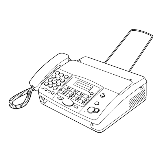
KX-FT902LS-B / KX-FT904LS-B 3 INSTALLATION 3.1. LOCATION OF CONTROLS 3.1.1. FRONT VIEW (1) Speaker (2) Document guides (3) Document tray (4) Paper stacker (KX-FT904LS-B ONLY) The paper stacker may not be shown in all illustrations in this operating instructions. (5) Document exit... -
Page 13: Control Panel
KX-FT902LS-B / KX-FT904LS-B 3.1.2. CONTROL PANEL programming. (1) [TONE] · To change from pulse to tone temporarily during dialling · To navigate to the next operation. when your line has rotary pulse services.. (18) [HELP] (7) [BROADCAST] (KX-FT904LS-B ONLY) · To print helpful information for quick reference. -
Page 14: Connections
KX-FT902LS-B / KX-FT904LS-B 3.2. CONNECTIONS (1) Handset cord. · The longer, uncoiled end should be connected to the unit. (2) Telephone line cord. · Connect to the single telephone line jack. (3) Power cord. · Connect to the power outlet (220-240 V, 50/60 Hz). -
Page 15: Installation
KX-FT902LS-B / KX-FT904LS-B 3.3. INSTALLATION 3.3.1. INSTALLATION SPACE The space required to install the unit is shown below. The dimensions given are necessary for the unit to operate efficiently. Note: · Avoid excessive heat or humidity. · Use the unit within the following ranges of temperature and humidity. -
Page 16: Recording Paper
KX-FT902LS-B / KX-FT904LS-B 3.3.3. RECORDING PAPER Open the cover by pressing the cover open button ( Close the cover securely by pushing down on. KX-FT902LS-B Install the recording paper. Press [FAX/START], then tear off the excess paper by pulling it towards you. - Page 17 KX-FT902LS-B / KX-FT904LS-B 3.3.4. DOCUMENTS THE UNIT CAN FEED Note: · Remove chips, staples or other similar fasteners. · Do not send the following types of documents. (Use the scanner glass for fax transmission.) — Chemically treated paper such as carbon or carbonless duplicating paper —...
-
Page 18: Setting Your Logo
KX-FT902LS-B / KX-FT904LS-B 3.3.5. SETTING YOUR LOGO The logo can be your name or the name of your company. Refer to TRANSLATION LISTS (P.3). To enter your logo Example: “BI LL” 1. Press [2] 2 times. 2. Press [4] 3 times. - Page 19 KX-FT902LS-B / KX-FT904LS-B 3.3.5.1. TO SELECT CHARACTERS WITH THE DIAL KEYPAD Pressing the dial keys will select a character as shown below. To select characters using Instead of pressing the dial keys, you can select characters using 1. Press repeatedly to display the desired character.
-
Page 20: Maintenance
KX-FT902LS-B / KX-FT904LS-B 4 MAINTENANCE 4.1. MAINTENANCE ITEMS AND COMPONENT LOCATIONS 4.1.1. OUTLINE MAINTENANCE AND REPAIRS ARE PERFORMED USING THE FOLLOWING STEPS. 1. Periodic maintenance Inspect the equipment periodically and if necessary, clean any contaminated parts. 2. Check for breakdowns Look for problems and consider how they arose. - Page 21 KX-FT902LS-B / KX-FT904LS-B 4.1.2.1. MAINTENANCE LIST OPERATION CHECK REMARKS Document Path Remove any foreign matter such as paper. — Rollers If the roller is dirty, clean it with a damp cloth then dry Refer to DOCUMENT FEEDER (P.23). thoroughly. Platen Roller If the platen is dirty, clean it with a damp cloth then dry —...
-
Page 22: Jams
KX-FT902LS-B / KX-FT904LS-B 4.2. JAMS 4.2.1. RECORDING PAPER JAMS When the recording paper has jammed in the unit The display will show the following. Refer to TRANSLATION LISTS (P.3). Open the cover by pressing the cover open button ( Cut off the wrinkled portion. -
Page 23: Cleaning
KX-FT902LS-B / KX-FT904LS-B 4.2.2. DOCUMENT JAMS - SENDING 4.3. CLEANING Open the cover by pressing the cover open button ( ) and 4.3.1. DOCUMENT FEEDER remove the jammed document carefully ( Clean the document feeder when: - Documents frequently misfeed. - Page 24 KX-FT902LS-B / KX-FT904LS-B 4.3.2. THERMAL HEAD If smudges or black/white lines appear on a copied/received document, check whether there is dust on the thermal head and head cover. Clean them to remove the dust. Disconnect the power cord and the telephone line cord.
-
Page 25: Disassembly Instructions
KX-FT902LS-B / KX-FT904LS-B 5 DISASSEMBLY INSTRUCTIONS 5.1. DISASSEMBLY FLOW CHART 5.1.1. UPPER CABINET SECTION CROSS REFERENCE: A-1 : HOW TO REMOVE THE PAPER STACKER (KX-FT904LS-B ONLY) (P.27) A-2 : HOW TO REMOVE THE OPERATION PANEL BLOCK (P.28) A-3 : HOW TO REMOVE THE OPERATION BOARD AND LCD (P.29) A-4 : HOW TO REMOVE THE IMAGE SENSOR (P.30) -
Page 26: Lower Cabinet Section
KX-FT902LS-B / KX-FT904LS-B 5.1.2. LOWER CABINET SECTION CROSS REFERENCE: A-1 : HOW TO REMOVE THE PAPER STACKER (KX-FT904LS-B ONLY) (P.27) A-2 : HOW TO REMOVE THE OPERATION PANEL BLOCK (P.28) B-1 : HOW TO REMOVE THE BOTTOM FRAME (P.33) B-2 : HOW TO REMOVE THE HANDSET CRADLE CABINET AND SPEAKER (P.34) B-3 : HOW TO REMOVE THE DIGITAL, ANALOG AND POWER SUPPLY BOARD AND AC INLET (P.35) -
Page 27: Disassembly Instructions
KX-FT902LS-B / KX-FT904LS-B 6 DISASSEMBLY INSTRUCTIONS 6.1. HOW TO REMOVE THE PAPER STACKER (KX-FT904LS-B ONLY) -
Page 28: How To Remove The Operation Panel Block
KX-FT902LS-B / KX-FT904LS-B 6.2. HOW TO REMOVE THE OPERATION PANEL BLOCK... -
Page 29: How To Remove The Operation Board And Lcd
KX-FT902LS-B / KX-FT904LS-B 6.3. HOW TO REMOVE THE OPERATION BOARD AND LCD... -
Page 30: How To Remove The Image Sensor
KX-FT902LS-B / KX-FT904LS-B 6.4. HOW TO REMOVE THE IMAGE SENSOR... -
Page 31: How To Remove The Thermal Head And Cutter Unit
KX-FT902LS-B / KX-FT904LS-B 6.5. HOW TO REMOVE THE THERMAL HEAD AND CUTTER UNIT... -
Page 32: How To Remove The Document Tray
KX-FT902LS-B / KX-FT904LS-B 6.6. HOW TO REMOVE THE DOCUMENT TRAY... -
Page 33: How To Remove The Bottom Frame
KX-FT902LS-B / KX-FT904LS-B 6.7. HOW TO REMOVE THE BOTTOM FRAME... -
Page 34: How To Remove The Handset Cradle Cabinet And Speaker
KX-FT902LS-B / KX-FT904LS-B 6.8. HOW TO REMOVE THE HANDSET CRADLE CABINET AND SPEAKER... -
Page 35: How To Remove The Digital, Analog And Power Supply Board And Ac Inlet
KX-FT902LS-B / KX-FT904LS-B 6.9. HOW TO REMOVE THE DIGITAL, ANALOG AND POWER SUPPLY BOARD AND AC INLET... -
Page 36: How To Remove The Rollers
KX-FT902LS-B / KX-FT904LS-B 6.10. HOW TO REMOVE THE ROLLERS... -
Page 37: How To Remove The Motor Block
KX-FT902LS-B / KX-FT904LS-B 6.11. HOW TO REMOVE THE MOTOR BLOCK... - Page 38 KX-FT902LS-B / KX-FT904LS-B CROSS REFERENCE: HOW TO REMOVE THE THERMAL HEAD AND CUTTER UNIT (P.31)
- Page 39 KX-FT902LS-B / KX-FT904LS-B...
-
Page 40: Installation Position Of The Lead Wires
KX-FT902LS-B / KX-FT904LS-B 6.12. INSTALLATION POSITION OF THE LEAD WIRES... -
Page 41: Installation Of Thermal Head
KX-FT902LS-B / KX-FT904LS-B 6.13. INSTALLATION OF THERMAL HEAD... -
Page 42: Troubleshooting Guide
KX-FT902LS-B / KX-FT904LS-B 7 TROUBLESHOOTING GUIDE 7.1. TROUBLESHOOTING SUMMARY 7.1.1. TROUBLESHOOTING After confirming the problem by asking the user, troubleshoot according to the instructions and observe the following precautions. 7.1.2. PRECAUTIONS 1. If there is a problem with the print quality or the paper feed, first check if the installation space and the print paper meets the specifications, the paper selection lever/paper thickness lever is set correctly, and the paper is set correctly without any slack. -
Page 43: User Recoverable Errors
KX-FT902LS-B / KX-FT904LS-B 7.2. USER RECOVERABLE ERRORS If the unit detects a problem, one or more of the following messages will appear on the display. The explanations given in the [ ] are for servicemen only. Refer to TRANSLATION LISTS (P.3). -
Page 44: Programming And Lists
KX-FT902LS-B / KX-FT904LS-B 7.3. PROGRAMMING AND LISTS The programming functions are used to program the various features and functions of the machine, and to test the machine. Programming can be done in both the on-hook and off-hook conditions. This facilitates communication between the user and the service while programming the machine. - Page 45 KX-FT902LS-B / KX-FT904LS-B 7.3.3. SERVICE FUNCTION TABLE Code Function Set Value Effective Range Default Remarks Setting the pause time 001~600 X 100 msec 001~600 Selects the pause time in 100 msec steps. Setting the flash recall time 01~99 X 10 msec...
- Page 46 KX-FT902LS-B / KX-FT904LS-B Code Function Set Value Effective Range Default Remarks Setting the overseas DIS 1: Detects on the 1st 1, 2 Sets the recognition format of the DIS signal. detection time.2: Detects on the 1:Detects the first DIS signal sent from the 2nd time.
-
Page 47: Test Functions
KX-FT902LS-B / KX-FT904LS-B 7.4. TEST FUNCTIONS Test Mode Type of Mode Code Function Operation after code input PRINT TEST Service Mode “8” “5” Prints a test pattern and checks the thermal head for abnormalities (missing dots, etc), and also checks the operation of the reception motor.(Refer to JOURNAL 3 START (P.84).) -
Page 48: Dtmf Single Tone Transmit Selection
KX-FT902LS-B / KX-FT904LS-B 7.4.1. DTMF SINGLE TONE TRANSMIT SELECTION When set to ON (=1), the 12 keys and transmission When set to OFF (=2), the 12 keys and transmission frequencies are as shown. frequencies are as shown. High Frequency (Hz) -
Page 49: Remote Programming
KX-FT902LS-B / KX-FT904LS-B 7.4.4. REMOTE PROGRAMMING If, after the call is connected, the customer describes the situation and it is determined that the problem can be corrected by making parameter changes, this function makes it possible to change parameters such as the user code and service code from another fax (using DTMF tones). - Page 50 KX-FT902LS-B / KX-FT904LS-B 7.4.4.2. PROGRAM MODE TABLE Code Function Set Value Default Remote setting Set the date and time mm/dd/yy 24H --------- Your logo --------- --------- Your fax number --------- --------- Print transmission report ERROR/ON/OFF ERROR Auto receive mode FAX ONLY / TEL/FAX...
- Page 51 KX-FT902LS-B / KX-FT904LS-B Code Function Set Value Default Remote setting Friendly reception CNG detection select 1:10S/2:20S/3:30S T1 timer 1:35 sec/2:60 sec 35 sec T4 timer 00~99 X 100ms Sensor check Press "START". --------- DTMF ON time 060~200ms 090ms DTMF OFF time...
- Page 52 KX-FT902LS-B / KX-FT904LS-B 7.4.5. USER MODE (The list below is an example of the SYSTEM SETUP LIST the unit prints out.) 7.4.5.1. KX-FT904LS-B Note: The above values are the default values.
- Page 53 KX-FT902LS-B / KX-FT904LS-B 7.4.5.2. KX-FT904LS-B Note: The above values are the default values.
- Page 54 KX-FT902LS-B / KX-FT904LS-B 7.4.6. SERVICE MODE SETTINGS (Example of a printed out list) 7.4.6.1. KX-FT902LS-B...
- Page 55 KX-FT902LS-B / KX-FT904LS-B 7.4.6.2. KX-FT904LS-B...
-
Page 56: Troubleshooting Details
KX-FT902LS-B / KX-FT904LS-B 7.5. TROUBLESHOOTING DETAILS 7.5.1. OUTLINE Troubleshooting guide provides a logical path of deduction to assist in locating a fault and suggests methods of restoring the unit to full working condition. Use the reported symptoms of the fault to determine the best troubleshooting method. Even difficult faults can be tracked to a specific block or area, for example, the "Digital Board"... - Page 57 KX-FT902LS-B / KX-FT904LS-B 7.5.3. TROUBLESHOOTING ITEMS TABLE FUNCTION SYMPTOM REFERENCE Printing Skewed receiving image See SKEWED RECEIVING IMAGE (P.63) Expanded print See EXPANDER PRINT (WHEN PRINTING) (P.64) Image is distorted See IMAGE IS DISTORTED (WHEN PRINTING) (P.62) Black or White vertical lines appear.
- Page 58 KX-FT902LS-B / KX-FT904LS-B 7.5.4. ADF (AUTO DOCUMENT FEED) SECTION 7.5.4.1. NO DOCUMENT FEED CROSS REFERENCE: DIGITAL BOARD SECTION (P.85) POWER SUPPLY BOARD SECTION (P.99) SENSOR SECTION (P.103) TEST FUNCTIONS (P.47) DISASSEMBLY INSTRUCTIONS (P.27)
-
Page 59: Document Jam
KX-FT902LS-B / KX-FT904LS-B 7.5.4.2. DOCUMENT JAM CROSS REFERENCE: SENSOR SECTION (P.103) DISASSEMBLY INSTRUCTIONS (P.27) - Page 60 KX-FT902LS-B / KX-FT904LS-B 7.5.4.3. MULTIPLE FEED When using thick paper etc., If the document will not feed. CROSS REFERENCE: DISASSEMBLY INSTRUCTIONS (P.27)
- Page 61 KX-FT902LS-B / KX-FT904LS-B 7.5.4.4. SKEW CROSS REFERENCE: DISASSEMBLY INSTRUCTIONS (P.27)
- Page 62 KX-FT902LS-B / KX-FT904LS-B 7.5.4.5. IMAGE IS DISTORTED (WHEN PRINTING) CROSS REFERENCE: READ SECTION (P.103) THERMAL HEAD SECTION (P.105) TEST FUNCTIONS (P.47) DISASSEMBLY INSTRUCTIONS (P.27)
- Page 63 KX-FT902LS-B / KX-FT904LS-B 7.5.4.6. BLACK OR WHITE VERTICAL LINES APPEAR CROSS REFERENCE: DIGITAL BOARD SECTION (P.85) TEST FUNCTIONS (P.47) 7.5.4.7. SKEWED RECEIVING IMAGE...
- Page 64 KX-FT902LS-B / KX-FT904LS-B 7.5.4.8. EXPANDER PRINT (WHEN PRINTING) CROSS REFERENCE: DISASSEMBLY INSTRUCTIONS (P.27) 7.5.4.9. WHEN COPYING OR PRINTING, AN ABNORMAL SOUND IS HEARD FROM THE UNIT...
- Page 65 KX-FT902LS-B / KX-FT904LS-B CROSS REFERENCE: DISASSEMBLY INSTRUCTIONS (P.27) 7.5.5. COMMUNICATION SECTION Find the problem in the table shown below, and refer to the corresponding troubleshooting procedure in DEFECTIVE FACSIMILE SECTION (P.66). Symptom Content Possible cause The paper is not fed properly when faxing.
- Page 66 KX-FT902LS-B / KX-FT904LS-B 7.5.5.1. DEFECTIVE FACSIMILE SECTION 7.5.5.1.1. TRANSMIT PROBLEM Refer to TRANSLATION LISTS (P.3). CROSS REFERENCE: ADF (AUTO DOCUMENT FEED) SECTION (P.58) OPERATION BOARD SECTION (P.102)
- Page 67 KX-FT902LS-B / KX-FT904LS-B 7.5.5.1.2. SOMETIMES THERE IS A TRANSMIT PROBLEM...
-
Page 68: Reception Problem
KX-FT902LS-B / KX-FT904LS-B 7.5.5.1.3. RECEPTION PROBLEM Confirm the following before starting troubleshooting. Is the recording paper installed properly? There is the receiving problem when sometimes the below errors may be occurred. OUT OF PAPER CHHECK COVER UNIT OVERHEATED (If it doesn´t return automatically, COVER OPEN, etc., reset the unit.) CHECK DOCUMENT Please refer to USER RECOVERABLE ERRORS (P.43) for the above items. - Page 69 KX-FT902LS-B / KX-FT904LS-B 7.5.5.1.4. THE UNIT CAN COPY, BUT CANNOT TRANSMIT/RECEIVE...
- Page 70 KX-FT902LS-B / KX-FT904LS-B 7.5.5.1.5. UNIT CAN COPY, BUT CANNOT TRANSMIT/RECEIVE LONG DISTANCE OR INTERNATIONAL COMMUNICATIONS The following 2 causes can be considered for this. Cause 1: The other party is executing automatic dialling, the call has been received by this unit, and the CED or DIS signal response time is too long.
- Page 71 KX-FT902LS-B / KX-FT904LS-B (Causes and Countermeasures) Countermeasure Side Echo Communication Problem Example Countermeasure Service Code Sending side Some time is needed to compare the level Add a dummy signal to the beginning Service code (521) of the receiving and sending signals for the of the training signal.
- Page 72 KX-FT902LS-B / KX-FT904LS-B Fig. c (Countermeasure by Changing the Interval Between CED and DIS) Fig. d (C3ountemeasure by Ignoring the 1st DIS) <TX side signal> <RX side signal> <Countermeasure> 2nd / 3rd DCS / Training & delayed CFR / FTT...
- Page 73 KX-FT902LS-B / KX-FT904LS-B 7.5.5.1.7. HOW TO RECORD FAX SIGNAL BY USING PC Recording FAX signal is one of the useful analysis measures to solve communication problems. The way of recording easily by using PC is shown as follows. 1. Equipment Parts No.
- Page 74 KX-FT902LS-B / KX-FT904LS-B 7.5.5.1.8. HOW TO OUTPUT THE JOURNAL REPORT: 1. Press repeatedly until the following is displayed. 2. Press 3. Press until the “ JOURNAL REPORT ” is displayed. 4. The report is printed out. Error code table: Refer to REPORTS (P.4).
- Page 75 KX-FT902LS-B / KX-FT904LS-B Countermeasure...
- Page 76 KX-FT902LS-B / KX-FT904LS-B...
- Page 77 KX-FT902LS-B / KX-FT904LS-B...
- Page 78 KX-FT902LS-B / KX-FT904LS-B...
- Page 79 KX-FT902LS-B / KX-FT904LS-B...
- Page 80 KX-FT902LS-B / KX-FT904LS-B...
- Page 81 KX-FT902LS-B / KX-FT904LS-B...
- Page 82 KX-FT902LS-B / KX-FT904LS-B...
- Page 83 KX-FT902LS-B / KX-FT904LS-B 7.5.6. OTHER [HISTORY] Display Function DATA Date and time which are set by a user for the first time after purchase. TIME is the expiration from the first power on after purchase. KEY OPERATION Indicate 2-digit codes. (Refer to BUTTON CODE TABLE (P.48).1st.50: History of the key operation from 1st to 50th after purchase.
- Page 84 KX-FT902LS-B / KX-FT904LS-B 7.5.7.1. JOURNAL 3 Descriptions: 1. ENCODE Compression Code: MH/MR 2. MSLT MSLT means Minimum Scan Line Time. Used only at the factory. 3. RESOLUTION (RESOL) Indicates the resolution of the communication. If multiple pages are transmitted or received, it indicates the last page´s resolution.
-
Page 85: Digital Board Section
KX-FT902LS-B / KX-FT904LS-B 7.5.8. DIGITAL BOARD SECTION One of most difficult problems to deal with is when the system will not boot up. The symptom: No response when the power is turned on. (No LCD display, keys are not accepted.) Note: 1. - Page 86 KX-FT902LS-B / KX-FT904LS-B 7.5.8.1. DIGITAL BLOCK DIAGRAM The signal lines that must be normal for the system to boot up For signal lines other than these, even if they malfunction they are listed here [List 1]. do not directly affect booting up the system.
- Page 87 KX-FT902LS-B / KX-FT904LS-B...
- Page 88 KX-FT902LS-B / KX-FT904LS-B Normal Wave Patterns Remarks: When you use an oscilloscope to judge whether a signal to be tested is normal or NG, perform the signal check in exactly the same order as in [List 1]. (If the ASIC fails to access the ROM, the ASIC cannot access SRAM normally.) The digital circuit actually operates according to the timing combinations of these signals.
- Page 89 KX-FT902LS-B / KX-FT904LS-B Note: Simply check the output level and make sure if the IC repeatedly outputs the signal at between 3.3V (H) and 0V (L). I/O and Pin No. Diagram...
- Page 90 KX-FT902LS-B / KX-FT904LS-B...
- Page 91 KX-FT902LS-B / KX-FT904LS-B After the power is turned on, the ASIC (CPU) initializes and checks each IC. The ROM, SRAM, and Modem are checked. If initialization fails for the ICs, the system will not boot up. CROSS REFERENCE: NG EXAMPLE (P.93)
- Page 92 KX-FT902LS-B / KX-FT904LS-B 7.5.8.2. FLASH MEMORY (IC6) (FT904 ONLY) If the unit is working correctly but the TAM fanction can not work, you should check the Flash Memory.
- Page 93 KX-FT902LS-B / KX-FT904LS-B 7.5.8.3. NG EXAMPLE...
- Page 94 KX-FT902LS-B / KX-FT904LS-B 7.5.8.4. CHECK THE STATUS OF THE DIGITAL BOARD First, please check voltages and oscillation whether they are correct as follows.
- Page 95 KX-FT902LS-B / KX-FT904LS-B...
- Page 96 KX-FT902LS-B / KX-FT904LS-B 7.5.9. ANALOG BOARD SECTION The analog parts check is actually different from the digital parts check. The signal route is determined by the purpose of the check. For example, the handset TX route begins from the handset microphone and is output in the telephone line. In this route, it is mainly an analog signal.
- Page 97 KX-FT902LS-B / KX-FT904LS-B Note: { }: Inside the digital board [ ]: Inside the operation board...
- Page 98 KX-FT902LS-B / KX-FT904LS-B 7.5.9.2. DEFECTIVE ITS (INTEGRATED TELEPHONE SYSTEM) SECTION...
- Page 99 KX-FT902LS-B / KX-FT904LS-B 7.5.10. POWER SUPPLY BOARD SECTION 1. Key components for troubleshooting Check the following parts first: F101, D101-D104, C106, Q101, PC101 and IC101. This comes from our experience with experimental tests. For example: power supply and lightning surge voltage test, withstanding voltage test, intentional short circuit test, etc.
- Page 100 KX-FT902LS-B / KX-FT904LS-B 2. Troubleshooting Flow Chart...
- Page 101 KX-FT902LS-B / KX-FT904LS-B 3. Broken parts repair details (D101, D102, D103, D104) Check for a short-circuit in terminal 4. If D101, D102, D103 and D104 are short-circuits, F101 will melt (open). In this case, replace all of the parts (D101, D102, D103, D104, F101).
- Page 102 KX-FT902LS-B / KX-FT904LS-B 7.5.11. OPERATION BOARD SECTION 7.5.11.1. NO KEY OPERATION CROSS REFERENCE: TEST FUNCTIONS (P.47) 7.5.11.2. NO LCD INDICATION CROSS REFERENCE: TEST FUNCTIONS (P.47)
- Page 103 KX-FT902LS-B / KX-FT904LS-B 7.5.12. SENSOR SECTION Refer to 6.5. SENSORS AND SWITCHES for the circuit descriptions. 7.5.12.1. CHECK THE DOCUMENT SENSOR (PS1)...."CHECK DOCUMENT" Refer to TRANSLATION LISTS (P.3). 7.5.12.2. CHECK THE READ POSITION (SW44)...."REMOVE DOCUMENT" Refer to TRANSLATION LISTS (P.3).
- Page 104 KX-FT902LS-B / KX-FT904LS-B CROSS REFERENCE: TEST FUNCTIONS (P.47)
- Page 105 KX-FT902LS-B / KX-FT904LS-B 7.5.14. THERMAL HEAD SECTION Refer to THERMAL HEAD (P.118). CROSS REFERENCE: SUPERVISION CIRCUIT FOR THE THERMAL HEAD TEMPERATURE (P.115) THERMAL HEAD (P.118)
-
Page 106: Circuit Operations
KX-FT902LS-B / KX-FT904LS-B 8 CIRCUIT OPERATIONS 8.1. CONNECTION DIAGRAM... -
Page 107: General Block Diagram
KX-FT902LS-B / KX-FT904LS-B 8.2. GENERAL BLOCK DIAGRAM The control section will be explained as shown in the block diagram. 1. ASIC (IC1) Composed mainly of an address decoder, modem control section, CPU and RTC. Controls the general FAX operations. Controls the operation panel I/F. - Page 108 KX-FT902LS-B / KX-FT904LS-B 8.2.1. GENERAL BLOCK DIAGRAM...
-
Page 109: Control Section
KX-FT902LS-B / KX-FT904LS-B 8.3. CONTROL SECTION 8.3.1. BLOCK DIAGRAM... - Page 110 KX-FT902LS-B / KX-FT904LS-B 8.3.2. ASIC (IC1) This custom IC is used for general FAX operations. 1. CPU This model uses a Z80 equivalent CPU operating at 8MHz. Many of the peripheral functions are handled by custom designed LSIs. As a result, the CPU only needs to process the result.
- Page 111 KX-FT902LS-B / KX-FT904LS-B SIGNAL POWER SUPPLIED DESCRIPTION VOLTAGE TONE2 3.3V TONE OUTPUT VOLUREF 3.3V ANALOG REF VOLTAGE VOLUOUT 3.3V VOLUME OUTPUT VOLUIN 3.3V VOLUME INPUT XNMI 3.3V HIGH FIXED FMEMDO/IOP 3.3V OUTPUT PORT (CIS ON) VDD (3.3V) ----- POWER SOURCE (+3.3V)
- Page 112 KX-FT902LS-B / KX-FT904LS-B SIGNAL POWER SUPPLIED DESCRIPTION VOLTAGE ADR12 3.3V CPU ADDRESS 12 RBA0 3.3V ROM/RAM BANK ADDRESS 0 RBA1 3.3V ROM/RAM BANK ADDRESS 1 RBA2 3.3V ROM/RAM BANK ADDRESS 2 RBA3 3.3V ROM/RAM BANK ADDRESS 3 RBA4 3.3V ROM/RAM BANK ADDRESS 4 RBA5 3.3V...
- Page 113 KX-FT902LS-B / KX-FT904LS-B 8.3.3. ROM (IC2) This 512 KB ROM (OTPROM or MASKROM) has 32 KB of common area and bank area (BK4~BK 63). The capacity of each bank is 8 KB. The addresses of the common area are from 0000H to 7FFFH, and addresses 8000H to 9FFFH are for the bank area.
- Page 114 KX-FT902LS-B / KX-FT904LS-B 8.3.6. SRAM and RTC BACK UP CIRCUIT 1. Function This unit has a lithium battery (BAT1) which works for the RAM (IC4) and Real Time Clock (RTC, Integrated into ASIC:IC1). The user parameter for auto dial numbers, the transmission ID, the system setup date and so on are stored in the RAM (IC4).
- Page 115 KX-FT902LS-B / KX-FT904LS-B 8.3.7. SUPERVISION CIRCUIT FOR THE THERMAL HEAD TEMPERATURE 1. Function The thermistor changes the resistor according to the temperature and uses the thermistor´s characteristics. The output of pin 139 of IC1 becomes a low level. Then when it becomes a high level, it triggers point (A).
-
Page 116: Facsimile Section
KX-FT902LS-B / KX-FT904LS-B 8.4. FACSIMILE SECTION 8.4.1. IMAGE DATA FLOW DURING FACSIMILE OPERATION COPY (Fine, Super-Fine, Photo) 1. Line information is read by CIS, via route (1), and is input to IC1. 2. In IC1, the data is adjusted to a suitable level for A/D conversion in the Analog Signal Processing Section, and via route (2) it is input to A/D conversion (8 bit). - Page 117 KX-FT902LS-B / KX-FT904LS-B 8.4.2. BLOCK DIAGRAM...
- Page 118 KX-FT902LS-B / KX-FT904LS-B 8.4.3. THERMAL HEAD 1. Function This unit utilizes state of the art thermal printer technology. The recording paper (roll paper) is chemically processed. When the thermal head contacts this paper it emits heat momentarily, and black dots (appearing like points) are printed on the paper. If this continues, letters and/or diagrams appear, and the original document is reproduced.
- Page 119 KX-FT902LS-B / KX-FT904LS-B...
- Page 120 KX-FT902LS-B / KX-FT904LS-B 8.4.4. SCANNING BLOCK The scanning block of this device consists of a control circuit and a contact image sensor made up of a celfoc lens array, an LED array, and photoelectric conversion elements. When an original is inserted and the start button pressed, pin 17 of IC1 goes to a high level and the transistor Q11 turns on and pin 129 of IC1 goes to a low level and the transistor Q7 turns on.
- Page 121 KX-FT902LS-B / KX-FT904LS-B 8.4.5. STEPPING MOTOR DRIVE CIRCUIT 1. Function One individual stepping motor is used for transmission and reception. It feeds the document or recording paper synchronized for reading or printing. 2. Circuit Operation During motor drive, gate array IC1 pin 124 becomes a high level, and Q4 and Q1 go ON as a result. +24 V is supplied to the motor coil.
-
Page 122: Gear Section
KX-FT902LS-B / KX-FT904LS-B 8.4.6. GEAR SECTION This section shows how the motor-driven gear mechanism works in the main operations: FAX transmission, FAX reception the motor and copying. 8.4.6.1. MODE SELECTION When the motor attached to the Drive Motor Gear rotates counterclockwise (CCW), Swing Gear A engages the CAM and the CAM turns counterclockwise to select a mode. - Page 123 KX-FT902LS-B / KX-FT904LS-B 8.4.6.2. MODE OPERATION Once a mode is selected, the Drive Motor Gear rotates clockwise (CW) and then the Swing Gear A-1 controls the mode operation. A: Transmit mode Swing Gear A-1 engages G6 and conveys its drive power to the Separation Roller Gear for pre-feeding documents.
- Page 124 KX-FT902LS-B / KX-FT904LS-B 8.4.6.3.2. SCANNING CROSS REFERENCE: SENSOR SECTION (P.103) 8.4.6.3.3. PRINTING Note: SENSORS AND SWITCHES (P.126)
- Page 125 KX-FT902LS-B / KX-FT904LS-B 8.4.6.3.4. COPYING CROSS REFERENCE: SENSOR SECTION (P.103)
-
Page 126: Sensors And Switches
KX-FT902LS-B / KX-FT904LS-B 8.5. SENSORS AND SWITCHES All of the sensors and switches are shown below. Sensor Circuit Sensor Sensor or Switch Name Message Error Location DIGITAL Motor Position [CALL SERVICE 2] CN6 (FT926 only) Cutter Position [PAPER JAMED] ANALOG... - Page 127 KX-FT902LS-B / KX-FT904LS-B 8.5.1. MOTOR POSITION SENSOR This sensor is a detection switch for recording the position of the CAM. Digital Board Signal (IC1-119 Pin) Home position Low level Other High level 8.5.2. CUTTER POSITION SENSOR (KX-FT904LS-B ONLY) Digital Board...
- Page 128 KX-FT902LS-B / KX-FT904LS-B 8.5.4. HOOK SWITCH (SW2) When the handset is lifted, the switch turns ON, and the signal at pin 43 of IC1 becomes low. When the handset is returned, the switch turns OFF, and the signal at pin 43 of IC1 becomes high.
- Page 129 KX-FT902LS-B / KX-FT904LS-B 8.5.6. DOCUMENT TOP SW (SW44) When a document is brought to the read position, the SW becomes ON, and the input signal of IC1-16 pin (Operation) becomes a low level. When there is no document at the read position, the SW becomes OFF, and the input signal of IC1-16 pin (Operation) becomes a high level.
-
Page 130: Modem Section
KX-FT902LS-B / KX-FT904LS-B 8.6. MODEM SECTION 8.6.1. FUNCTION The unit uses a 1 chip modem (IC5), enabling it to act as an interface between the control section for FAX sending and receiving, and the telephone line. During a sending operation, the digital image signals are modulated and sent to the telephone line. - Page 131 KX-FT902LS-B / KX-FT904LS-B 3. Facsimile Call Time Series As shown in the following diagram, the facsimile call time series is divided into five phases. Phase A : Call setting Call setting can be manual/automatic. Phase B : Pre-message procedure Phase B is a pre-processing procedure and sequence for confirming the status of the terminal, transmission route, etc. and for terminal control.
- Page 132 KX-FT902LS-B / KX-FT904LS-B 6. Explanation of Technology a. G3 Communication Signals (T. 30 Binary Process) For G3 facsimile communication, this is the procedure for exchanging control signals between the sending and receiving machines both before and after transmission of image signals.
- Page 133 KX-FT902LS-B / KX-FT904LS-B (Example) Bit No. DIS/DTC Transmitter - T.2 operation Receiver - T.2 operation Receiver - T.2 operation T.2 IOC = 176 T.2 IOC = 176 Transmitter - T.3 operation Receiver - T.3 operation Receiver - T.3 operation Reserved for future T.3 operation features.
- Page 134 KX-FT902LS-B / KX-FT904LS-B Bit No. DIS/DTC Standard setting Recording width capability 1216 picture elements along Middle 1216 elements of 1728 picture elements scan line length of 151 ± mm 1% Recording width capability 864 picture elements along Middle 864 elements of 1728 picture elements scan line length of 107 ±...
- Page 135 KX-FT902LS-B / KX-FT904LS-B b. Redundancy Compression Process Coding Mode This unit uses one-dimensional MH format.
- Page 136 KX-FT902LS-B / KX-FT904LS-B 8.6.2. MODEM CIRCUIT OPERATION The modem (IC5) has all the hardware satisfying the ITU-T standards mentioned previously. When the ASIC IC1 (61) is brought to a low level, the modem (IC5) is chip-selected and the resistors inside IC are selected by the select signals from ASIC (IC1) ADR0-ADR4.
-
Page 137: Analog Unit Block Diagram
KX-FT902LS-B / KX-FT904LS-B 8.7. ANALOG UNIT BLOCK DIAGRAM... -
Page 138: Ncu Section
KX-FT902LS-B / KX-FT904LS-B 8.8. NCU SECTION 8.8.1. GENERAL This section is the interface between the telephone line. It is composed of bell detection circuit, pulse dialing circuit, CPC detection circuit, line amplifier, sidetone circuits and Remote FAX activation circuit. 8.8.2. - Page 139 KX-FT902LS-B / KX-FT904LS-B 8.8.5. LINE AMPLIFIER AND SIDE TONE CIRCUITS 1. Circuit Operation The reception signal received as output from line transformer T1 is given as input to C17, R13 and IC3(2). Then it is input to the reception system at an amplifier gain of 2.5 dB from pin (2).
-
Page 140: Its (Integrated Telephone System) And Monitor Section
KX-FT902LS-B / KX-FT904LS-B 8.9. ITS (INTEGRATED TELEPHONE SYSTEM) AND MONITOR SECTION 8.9.1. GENERAL The general ITS operation is performed by the modem IC5. The alarm tone, the key tone, the calling tone and the beep are output from the ASIC IC1 (digital board). - Page 141 KX-FT902LS-B / KX-FT904LS-B 8.10.2. CIRCUIT DIAGRAM...
-
Page 142: Operation Board Section
KX-FT902LS-B / KX-FT904LS-B 8.11. OPERATION BOARD SECTION The unit consists of an LCD (Liquid crystal display), KEYs and LED (light-emitting diode). They are controlled by the Gate Array (IC1) and ASIC (IC1: on the DIGITAL BOARD). The key matrix table is shown below. -
Page 143: Lcd Section
KX-FT902LS-B / KX-FT904LS-B 8.12. LCD SECTION The Gate Array (IC1) works only for writing the ASCII code from data bus (D4-D7). V0 is supplied for the crystal drive. R13 and R14 are density control resistors. Consequently, in this unit, the timing (positive clock) is generated by the LCD interface circuitry in the gate array (IC1). -
Page 144: Power Supply Board Section
KX-FT902LS-B / KX-FT904LS-B 8.13. POWER SUPPLY BOARD SECTION This power supply board uses the switching regulator method. Block Diagram Input Input Rectifier Circuit C106 R136 Output Circuit Kick-on Surge Circuit R137 Voltage absorber Circuit Converter circuit Circuit A-B Voltage Wave Form... - Page 145 KX-FT902LS-B / KX-FT904LS-B The following is an overview of how the power supply unit is controlled. The control method of this power supply unit is pulse width modulation. When Q is ON, the energy is charged in the transfer primary coil according to E .
- Page 146 KX-FT902LS-B / KX-FT904LS-B [Surge Absorber Circuit] This circuit is for absorbing surge voltage generated by the transformer. [Control Circuit and Detecting Circuit] The control circuit amplifies the output with increased voltage detected in the error detecting circuit. Then it drives the main transistor.
-
Page 147: Reference Material Data
KX-FT902LS-B / KX-FT904LS-B 9 REFERENCE MATERIAL DATA 9.1. TERMINAL GUIDE OF THE ICs TRANSISTORS AND DIODES... -
Page 148: How To Replace The Flat Package Ic
KX-FT902LS-B / KX-FT904LS-B 9.2. HOW TO REPLACE THE FLAT PACKAGE IC Even if you do not have the special tools (for example, a spot heater) to remove the Flat IC, with some solder (large amount), a soldering iron and a cutter knife, you can easily remove the ICs that have more than 100 pins. -
Page 149: Flat Package Ic Installation Procedure
KX-FT902LS-B / KX-FT904LS-B 9.2.3. FLAT PACKAGE IC INSTALLATION PROCEDURE 1. Temporarily fix the FLAT PACKAGE IC, soldering the two marked pins. *Check the accuracy of the IC setting with the corresponding soldering foil. 2. Apply flux to all pins of the FLAT PACKAGE IC. -
Page 150: Test Chart
KX-FT902LS-B / KX-FT904LS-B 9.3. TEST CHART 9.3.1. ITU-T No.1 TEST CHART... - Page 151 KX-FT902LS-B / KX-FT904LS-B 9.3.2. ITU-T No.2 TEST CHART...
-
Page 152: Fixtures And Tools
KX-FT902LS-B / KX-FT904LS-B 10 FIXTURES AND TOOLS... -
Page 153: Cabinet, Mechanical
KX-FT902LS-B / KX-FT904LS-B 11 CABINET, MECHANICAL 11.1. OPERATION PANEL SECTION... -
Page 154: Upper Cabinet Section
KX-FT902LS-B / KX-FT904LS-B 11.2. UPPER CABINET SECTION... -
Page 155: Lower Cabinet
KX-FT902LS-B / KX-FT904LS-B 11.3. LOWER CABINET CROSS REFERENCE: MOTOR SECTION (P.156) -
Page 156: Motor Section
KX-FT902LS-B / KX-FT904LS-B 11.4. MOTOR SECTION 11.4.1. KX-FT902LS-B... - Page 157 KX-FT902LS-B / KX-FT904LS-B 11.4.2. KX-FT904LS-B...
-
Page 158: Actual Size Of Screws
KX-FT902LS-B / KX-FT904LS-B 11.5. ACTUAL SIZE OF SCREWS... -
Page 159: Accessories And Packing Materials
KX-FT902LS-B / KX-FT904LS-B 12 ACCESSORIES AND PACKING MATERIALS... -
Page 160: Replacement Parts List
KX-FT902LS-B / KX-FT904LS-B 13 REPLACEMENT PARTS LIST 1. RTL (Retention Time Limited) Ref. Part No. Part Name & Description Remarks Note: PFDG1123Z GEAR, PLATEN The marking (RTL) indicates that the Retention Time is PFDJ1021Z PLATEN SPACER, R POM-HB PFDN1033Z ROLLER, PLATEN limited for this item. -
Page 161: Digital Board Parts
KX-FT902LS-B / KX-FT904LS-B Ref. Part No. Part Name & Description Remarks 13.1.3. LOWER CABINET PFDG1362Z GEAR,D (KX-FT902LS-B) POM-HB Ref. Part No. Part Name & Description Remarks 13.1.5. ACCESSORIES AND PACKING PFHA1001Z RUBBER,LEG PFMD1075Z FRAME,BOTTOM MATERIALS PFDF1051Z SHAFT POM-HB PFDE1133Z SPACER POM-HB Ref. - Page 162 KX-FT902LS-B / KX-FT904LS-B Ref. Part No. Part Name & Description Remarks Ref. Part No. Part Name & Description Remarks PQJP02G100Z CONNECTOR, 2 PIN ERJ3GEYJ4R7 ERJ3GEYJ222 2.2K (COILS) ERJ3GEYJ203 PQLQR2KA20T COIL ERJ3GEYJ472 4.7K PQLQR2KA20T COIL ERJ3GEYJ333 J0JCC0000042 COIL ERJ3GEYJ101 J0JCC0000042 COIL...
- Page 163 KX-FT902LS-B / KX-FT904LS-B Ref. Part No. Part Name & Description Remarks Ref. Part No. Part Name & Description Remarks PQCUV1H104ZF C120 ECUV1E104ZFV ECEA1CK101 C123 ECEA1HKA4R7 ECUV1H102KBV 0.001 C126 ECUV1H102KBV 0.001 ECUV1E104ZFV C127 ECUV1C104KBV ECUV1E104ZFV C129 ECUV1C104KBV ECUV1E104ZFV ECUV1H101JCV 100P 13.2.2. KX-FT904LS-B...
- Page 164 KX-FT902LS-B / KX-FT904LS-B Ref. Part No. Part Name & Description Remarks Ref. Part No. Part Name & Description Remarks EXB38V101JV RESISTOR ARRAY ERJ3GEYJ102 EXB38V101JV RESISTOR ARRAY ERJ3GEY0R00 EXB38V101JV RESISTOR ARRAY ERJ3GEYJ470 ERJ3GEYJ105 (CRYSTAL OSCILLATORS) ERJ3GEYJ104 100K PFVCCFS32Z CRYSTAL OSCILLATOR ERJ3GEYJ103...
-
Page 165: Analog Board Parts
KX-FT902LS-B / KX-FT904LS-B Ref. Part No. Part Name & Description Remarks Ref. Part No. Part Name & Description Remarks ECUV1H102KBV 0.001 PQVTDTC114EU TRANSISTOR(SI) ECUV1H150JCV PQVTDTC114EU TRANSISTOR(SI) ECUV1E104ZFV 2SB1218ARL TRANSISTOR(SI) ECUV1E104ZFV PQVTDTC114EU TRANSISTOR(SI) ECUV1H120JCV PQVTDTC114EU TRANSISTOR(SI) ECUV1E104ZFV 2SC2235 TRANSISTOR(SI) ECUV1E104ZFV 2SC4155R... -
Page 166: Operation Board Parts
KX-FT902LS-B / KX-FT904LS-B Ref. Part No. Part Name & Description Remarks Ref. Part No. Part Name & Description Remarks ERJ3GEY0R00 ERDS1TJ184 180K ERJ3GEY0R00 ERJ3GEYJ105 ERJ3GEY0R00 ERJ3GEY0R00 (CAPACITORS) ERJ3GEY0R00 ECUV1H103KBV 0.01 ERJ3GEY0R00 ECUV1H103KBV 0.01 ERJ3GEY0R00 ECEA1HKA4R7 ERJ3GEY0R00 ECUV1H103KBV 0.01 ERJ3GEYJ101 ECEA0JKA470... -
Page 167: Power Supply Board Parts
KX-FT902LS-B / KX-FT904LS-B Ref. Part No. Part Name & Description Remarks 13.5. POWER SUPPLY BOARD EVQ11Y05B SWITCH PARTS EVQ11Y05B SWITCH EVQ11Y05B SWITCH Ref. Part No. Part Name & Description Remarks EVQ11Y05B SWITCH EVQ11Y05B SWITCH PCB4 N0AC2GJ00004 POWER SUPPLY BOARD ASS´Y... -
Page 168: Fixtures And Tools
KX-FT902LS-B / KX-FT904LS-B Ref. Part No. Part Name & Description Remarks R203 ERDS1FVJ470 R221 ERJ3GEYJ222 2.2k R222 ERJ3GEYJ222 2.2k R223 ERJ3GEYJ101 R224 ERJ3GEYJ273 R225 ERJ3GEYJ332 3.3k (CAPACITORS) C101 ECQU2A224MV 0.22 C102 ECQU2A104MV C103 PFKD2E3KH102 0.001 C105 PFKD2E3KH222 0.0022 C106 UEB2W560U... -
Page 169: Printed Circuit Board
KX-FT902LS-B / KX-FT904LS-B... - Page 170 KX-FT902LS-B / KX-FT904LS-B XTEST...
-
Page 171: Analog Board (Pcb2)
KX-FT902LS-B / KX-FT904LS-B FLT3... - Page 172 KX-FT902LS-B / KX-FT904LS-B +2.0V...
-
Page 173: Operation Board (Pcb3)
KX-FT902LS-B / KX-FT904LS-B... - Page 174 KX-FT902LS-B / KX-FT904LS-B...
-
Page 175: Power Supply Board (Pcb4)
KX-FT902LS-B / KX-FT904LS-B... -
Page 176: For The Schematic Diagrams
KX-FT902LS-B / KX-FT904LS-B 15 FOR THE SCHEMATIC DIAGRAMS Note: 1. DC voltage measurements are taken with an oscilloscope or a tester with a ground. 2. The schematic diagrams and circuit board may be modified at any time with the development of new technology. -
Page 177: Memo
KX-FT902LS-B / KX-FT904LS-B 16 MEMO... -
Page 178: Schematic Diagram
KX-FT902LS-B / KX-FT904LS-B 17 SCHEMATIC DIAGRAM 17.1. DIGITAL BOARD (PCB1) 17.1.1. KX-FT902LS-B +3.3V/BATIN C114 Z0.1u MOTOR BLOCK +24V 4M ROM 1M SRAM A[0] D[0] RBA[4] RBA[3] A[1] D[1] RBA[2] A[2] D[2] +5VD RBA[0] A[3] D[3] 9 A3 A[7] RBA[1] A[4]... - Page 179 CIS BLOCK R103 +5VA 2.1V +3.3VD R118 IC12 (26) +24V1 100K 1 CD 2 FC2 3 FC1 4 VIN +3.3VD C126 K1000p CIS Power K0.1u R116 R117 C127 ON: 0V OFF: 3.3V TO CIS KX-FT902LS-B : DIGITAL BOARD (27)
- Page 180 KX-FT902LS-B / KX-FT904LS-B 17.1.2. KX-FT904LS-B +3.3V/BATIN C114 Z0.1u MOTOR BLOCK +24V 4M ROM 1M SRAM A[0] D[0] RBA[4] RBA[3] A[1] D[1] RBA[2] A[2] D[2] +5VD RBA[0] A[3] 9 A3 D[3] A[7] RBA[1] A[4] 8 A4 D[4] A[6] A[8] A[5] 7 A5...
- Page 181 KX-FT902LS-B / KX-FT904LS-B TAD MODEL ONLY FAX TX 4M FLASH for VOICE FAX RX A[0] 20 A0 D[0] A[1] 19 A1 D[1] A[2] 18 A2 D[2] +24V1 +5VA A[3] 17 A3 D[3] A[4] D[4] 16 A4 +5VA A[5] 15 A5...
-
Page 182: Analog Board (Pcb2)
KX-FT902LS-B / KX-FT904LS-B 17.2. ANALOG BOARD (PCB2) 1.5K FAX TX Signal 2.0V FAX RX Signal +24VA HANDSET, MONITOR FAX RX 100K +2.0V 10uF 16V J180p R13 75K K0.022u Z0.1u 300:600 50V4.7u +12V R18 75K 5.6V K0.022u 4.7V IC3-1 5.6V 100K 2.7K... - Page 183 KX-FT902LS-B / KX-FT904LS-B FAX TX Signal FAX RX Signal 680p 6.8K 680p 10uF 50V BEAD 50V4.7u W5NL5T ZNR1 300V/310V 120V TH1 NC RLY1-1 POS1 BEAD 2.2K 3000V 6.2K BEAD 250V1u BEAD 5.6V 5.6V 15K 1/2W J180p 390K +2.0V 10:1 IC2-1...
-
Page 184: Operation Board (Pcb3)
KX-FT902LS-B / KX-FT904LS-B... -
Page 185: Power Supply Board (Pcb4)
KX-FT902LS-B / KX-FT904LS-B... - Page 186 KX-FT902LS-B / KX-FT904LS-B KXFT902LSB KXFT904LSB...
Need help?
Do you have a question about the KX-FT902LS-B and is the answer not in the manual?
Questions and answers