Advertisement
Quick Links
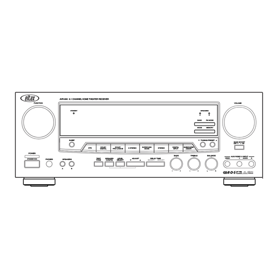
AVR-800
6.1 Channel
Home Theatre Receiver
SERVICE MANUAL
CONTENTS
Specifications .......................................................... 2
Measurements And Adjustments ............................ 3
Troubleshooting....................................................... 5
IC Internal Diagrams ............................................... 6
Electrical Parts List................................................ 27
Block Diagram ....................................................... 33
Wiring Diagram...................................................... 35
Schematic Diagrams ............................................. 37
Printed Circuit Boards ........................................... 45
Exploded View....................................................... 53
Advertisement

Related Manuals for Eltax AVR-800


Summary of Contents for Eltax AVR-800
-
Page 1: Table Of Contents
AVR-800 6.1 Channel Home Theatre Receiver SERVICE MANUAL CONTENTS Specifications ............2 Measurements And Adjustments ......3 Troubleshooting............5 IC Internal Diagrams ..........6 Electrical Parts List..........27 Block Diagram ............33 Wiring Diagram............35 Schematic Diagrams ..........37 Printed Circuit Boards ........... 45... -
Page 2: Specifications
SPECIFICATIONS Amplifier Section AM Tuner Section Output Power Tuning Range: Stereo Mode : 120W/CH 522 kHz – 1,620 kHz (9 kHz steps) Usable Sensitivity: 55 dB/m (1% THD 1KHz 8ohm DIN) Total Harmonic Distortion: 0.8% at 85 dB/m Surround Mode : 92W/CH Signal-to-Noise Ratio: 45 dB at 85 dB/m (1% THD 1KHz 8ohm DIN) Video Section... -
Page 3: Measurements And Adjustments
MEASUREMENTS AND ADJUSTMENTS ALIGNMENT INSTRUCTIONS EQUIPMENT NEEDED AM Signal Generator FM Signal Generator Oscilloscope VTVM(AC,DC) Test loop antenna(AM Adjustment) Dummy antenna(FM Adjustment) IMPORTANT 1.Check power-source voltage. 2.Set the function switch to band aligned. 3.Keep the signal input as low as possible to adjust accurately. 4.Modulation and modulation frequency. - Page 4 ■ FM/AM AUTO STOP LEVEL ADJUSTMENT FM Signal Generator ..Connect to FM ANT Jack (FM IN) through the dummy. AM Signal Generator ..Connect to AM ANT. Coil the through the Loop anten Signal Generator Adjust for Adjustment...
-
Page 5: Troubleshooting
TROUBLESHOOTING Problem Probable Cause Remedy Amplifier When listening to the music in stereo, Speakers are connected wrong. After checking, if needed, reconnect. left/right speakers sounds reversed. Low hum or buzzer sound. Power line of a fluorescent light is installed Place this product as far away as possible near this product. -
Page 6: Ic Internal Diagrams
IC INTERNAL DIAGRAMS TC9163AF (FUNCTION/INPUT) : IC51 BLOCK DIAGRAM TC9164AF (FUNCTION/INPUT) : IC53 BLOCK DIAGRAM L-COM R-COM L-COM R-COM L-COM R-COM DATA SHIFT REGISTER - 6 -... - Page 7 TC9162AF (FUNCTIOIC TC9162AF (FUNCTION/INPUT) : IC54 BLOCK DIAGRAM BLOCK DIAGRAM L-COM L-COM R-COM R-COM L-COM L-COM R-COM R-COM L-COM L-COM R-COM R-COM L-COM L-COM R-COM R-COM DATA DATA SHIFT REGISTER SHIFT REGISTER TC9459F(VOLUME) : IC55 BLOCK DIAGRAM - 7 -...
- Page 8 M62446FP(VOLUME) : IC56 BLOCK DIAGRAM PIN CONFIGRATION - 8 -...
- Page 9 AK5381 (A/D∑ CONVERTER) : IC57 AGND DGND MCLK Clock Divider ∆Σ Decimation AINL Modulator Filter LRCK SCLK ∆Σ Decimation AINR Modulator Filter Serial I/O SDTO Interface VCOM Voltage Reference CKS2 CKS1 CKS0 PIN / FUNCTION No. Pin Name Function AINR Rch Analog Input Pin AINL Lch Analog Input Pin...
- Page 10 AK4358 (D/A CONVERTER) : IC58 Audio LOUT1+ MCLK DATT LOUT1- LRCK BICK ROUT1+ SDTI1 DATT ROUT1- SDTI2 SDTI3 LOUT2+ SDTI4 DATT LOUT2- ROUT2+ Control 3-wire DATT ROUT2- Register or I2C LOUT3+ DATT DCLK LOUT3- DSDL1 ROUT3+ DSDR1 DATT DSDL2 ROUT3- DSDR2 LOUT4+ DSDL3...
- Page 11 PIN DESCRIPTION Pin Name Function LOUT1- DAC 1 Lch Negative Analog Output Pin LOUT1+ DAC 1 Lch Positive Analog Output Pin DZF3 Zero Input Detect 3 Pin DZF2 Zero Input Detect 2 Pin DZF1 Zero Input Detect 1 Pin CAD0 Chip Address 0 Pin Auto Setting Mode Disable Pin(Pull-down Pin) ACKSN...
- Page 12 AUDIO DSP (CS493264 - CLG) : IC59 PIN ASSIGNMENT.(CS493264) DGND1 MCLK AUDATA3, XMT958 SCLK WR,DS,EMWR,GPIO10 LRCLK RD,R/W,EMOE,GPIO11 AUDATA0 A1,SCDIN AUDATA1 A0,SCCLK AUDATA2 6 5 4 3 2 1 44 43 42 41 40 DATA7,EMAD7,GPIO7 DATA6,EMAD6,GPIO6 DATA5,EMAD5,GPIO5 RESET DATA4,EMAD4,GPIO4 AGND CS493XXX-CLG 44-pin PLCC Top View DGND2...
- Page 13 PIN DESCRIPTION.(CS493264) PIN No. Pin Name Function 1,12,23 +VD1 Digital Power supply. Normally +2.5v 2,13,24 DGND Digital Ground AUD3 SPDIF transmitter output/Digital audio output(N.C) Host write strobe pin(connected to GND with an external resistor) Host parallel output enable pin(pulled up with an external resistor) CS_DA SPI Serial data input pin CS_CK...
- Page 14 TC74HCU04(INVERTER) : IC60 - 14 -...
- Page 15 AK4114VQ(DIR) : IC66 TOP VIEW INT0 IPS0/RX4 AVSS OCKS0/CSN/CAD0 OCKS1/CCLK/SCL DIF0/RX5 CM1/CDTI/SDA TEST2 AK4114VQ DIF1/RX6 CM0/CDTO/CAD1 AVSS DIF2/RX7 Top View IPS1/IIC DAUX P/SN XTL0 MCKO2 BICK XTL1 SDTO BLOCK DIAGRAM AVSS AVDD X'tal Clock Oscillator 8 to 3 Recovery Clock MCKO1 Generator MCKO2...
- Page 16 DIR IC PIN FUNCTION PIN/FUNCTION Pin Name Function IPS0 Input Channel Select 0 Pin in Parallel Mode Receiver Channel 4 Pin in Serial Mode (Internal biased pin) No Connect NC(AVSS) No internal bonding. This pin should be connected to AVSS. DIF0 Audio Data Interface Format 0 Pin in Parallel Mode Receiver Channel 5 Pin in Serial Mode (Internal biased pin)
- Page 17 PIN/FUNCTION (Continued) Pin Name Function Power-Down Mode Pin When “L”, the AK4114 is powered-down and reset. Master Clock Operation Mode 0 Pin in Parallel Mode CDTO Control Data Output Pin in Serial Mode, IIC= “L”. CAD1 Chip Address 1 Pin in Serial Mode, IIC= “H”. Master Clock Operation Mode 1 Pin in Parallel Mode CDTI Control Data Input Pin in Serial Mode, IIC= “L”.
- Page 18 LA7952 (VIDEO SWITCH) : IC77,78 NJM2296M (VIDEO SWITCH) : IC79 BLOCK DIAGAM Vin1 Vin2 Vout1 6.2dB dirver Vin3 6.2dB Vout2 dirver Vin4 Vout3 6.2dB dirver Vin5 - 18 -...
- Page 19 MB90F476AFPG(FLASH U-COM) : IC91 BLOCK DIAGAM Clock control X0, X1 RSTX circuit X0, X1A core MC-16LX family Interrupt controller PPG0, 1 PPG2, 3 8-/16-bit PPG PPG4, 5 AIN0, 1 BIN0, 1 8-/16-bits UD counter Communication prescaler ZIN0, 1 EXTC SIN0 µPG MT00 UART...
- Page 20 TOP VIEW P 20/A16 P 21/A17 P22/A18 P57/CLK P23/A19 RSTX P24/A20/PPG0 P56/RDY P 25/A21/PPG1 P55/HAKX P26/A22/PPG2 P54/HRQ P27 /A23/PPG3 P53/WRHX P30 /A00/AIN0 P52/WRLX P 31/A01/BIN0 P51/RDX P50/ALE P32/A02/ZIN0 PA3/OUT3 P33 /A03/AIN1 PA2/OUT2 P 34/A04/BIN1 PA1/OUT1 Q F P - 1 0 0 P35/A05/ZIN1 PA0/OUT0 (TOP VIEW)
- Page 21 PIN FUNCTIONS PIN No. SYMBOL DESCRIPTION F-STB Function IC(TC9163/TC9164) STB Output Port F-DATA Function IC(TC9163/TC9164) DATA Output Port PLL-CE PLL IC(LC72131,on the Tuner Module) Chip Enable Control Port F-CLK Function IC(TC9163/TC9164) CLOCK Output Port PLL D/I PLL IC(LC72131,on the Tuner Module) Data Input Port TUNE Tuned Display Control Port(Active "L") STEREO...
- Page 22 PIN No. SYMBOL DESCRIPTION VFD-CS VFD Chip Selector Out Port VFD-BLK VFD BLK Out Port REMOTE-OUT Remote Control Data Output Port POWER-H Power ON/OFF Control Port(Active"H") SURR-H Surround ON/OFF Control Port(Active"H") 65,69,70,71,72 OPTION Option Control Port VOL-DOWN Master Volume Up/Down Control Port VOL-UP FUNC-DOWN Function UP/DOWN Control Port...
- Page 23 LC75725E (VFD DRIVER) : IC92 TOP VIEW BLOCK DIAGAM - 23 -...
- Page 24 PIN FUNCTIONS Pin No. Function Handling when unused 1, 13 Driver block power supply connection. (Both pins must be connected.) — — Logic block power supply connection. Provide a voltage between 4.5 and 5.5 V. — — Power supply connection. Connect to the ground. —...
- Page 25 RE5VT15CATZ(RESET) : IC96 BLOCK DIAGAMS - 25 -...
- Page 26 PRODUCT SAFETY NOTICE Many electical and mechanical parts in the appliance have special safety related characteristics. These are often not evident from visual inspection nor the protection afforded by them necessarily can be obtained by using replacement components rated for voltage, wattage, etc. replacement parts which have these special safety characteristics are identified in this Service Manual.
-
Page 27: Electrical Parts List
ELECTRICAL PARTS LIST REF. NO. PARTS NO. DESCRIPTION REMARKS FORONT PCB ASS'Y COP11598B PCB , FRONT ASS'Y CIP11598B PCB , FRONT AUTO ASS'Y CUP11598Y PCB , FRONT D901-905 HVD1SS133MT DIODE 1SS133T-77 D906 HVDMTZJ5.1BT DIODE , ZENER 5.1V 1/2W D907-909 HVD342VCTB7T089 L.E.D , RED SLR342VCTB7T089 D910... - Page 28 REF. NO. PARTS NO. DESCRIPTION REMARKS SW82 KSH2B003Z SW , PUSH(VERTICAL) VE81 HSR2A004Z VR , ENCODER EC16B243040HB VE91 HSR2A006Z VR , ENCODER EC16B1220408A VR91 CVV2W03M104Z RES , VARIABLE(100KMN) RK14K1260102 VR92,93 CVV2W04C104Z RES , VARIABLE(100KCX2) RK14K1260102 X901 HOX04194E120TF CRYSTAL , OSC HC-49/S(ATS) X902 HOX04332E200C...
- Page 29 REF. NO. PARTS NO. DESCRIPTION REMARKS Q126 HVTKTD600KGR T.R , BIAS KTD600KGR Q130 HVT2SC3856 T.R , POWER 2SC3856 Q131 HVT2SA1492 T.R , POWER 2SA1492 Q142 HVTKTD600KGR T.R , BIAS KTD600KGR Q146 HVT2SC4468 T.R , POWER 2SC4466 Q147 HVT2SA1695 T.R , POWER 2SA1695 Q158 HVTKTD600KGR...
- Page 30 REF. NO. PARTS NO. DESCRIPTION REMARKS Q193 HVTKTB1369Y T.R , DRIVE KTB1369Y RY11-13 HSL4A004ZU RELAY OSA-SS-212DM3 RY81 HSL4A011ZE RELAY OMI-SS-212L R137 CRF5EKR22HX2 RES , CEMENT 0.22OHM(*2), 5W R142 CRG1ANJ100H RES , METAL OXIDE FILM 10 OHM 1W R181 CRF5EKR22HX2 RES , CEMENT 0.22OHM(*2), 5W R186 CRG1ANJ100H...
- Page 31 REF. NO. PARTS NO. DESCRIPTION REMARKS JK41-43 CJJ4P014W JACK , IN/OUT JK44 CJJ4R019W TERMINAL , IN/OUT JK45 CJJ4N068Z JACK , BOARD JK46 HJS9L001Z MODULE, OPTICAL TOTX178 JK47,48 HJSTORX179 MODULE , OPTICAL TORX179 JK49 CJJ4R038Z JACK , BOARD L701,702 KLZ9H001Z BEAD , CORE L704,705 KLZ9H001Z BEAD , CORE...
- Page 32 REF. NO. PARTS NO. DESCRIPTION REMARKS C771 HCEA1EH331T CAP , ELECT 330UF 25V C774 HCEA1EH471E CAP , ELECT 470UF 25V C776 KCKDKS472ME CAP , CERAMIC 0.0047UF/2.5KV IC77 BVILA7952 I.C , VCR FUNC LA7952 IC78 BVILA7952 I.C , VCR FUNC LA7952 IC79 HVINJM2296M I.C , VIDEO SW...
Need help?
Do you have a question about the AVR-800 and is the answer not in the manual?
Questions and answers