Table of Contents
Advertisement
VOICE GUIDE & STORAGE UNIT
VGS-1
SERVICE MANUAL
Recording/Playback Operation .................................................................... 2
I/O Ports ......................................................................................................... 2
Beat Shift Circuit ........................................................................................... 3
Amateur Transceiver Identification ............................................................. 3
MCU : HD6433024D01TE (IC2) ...................................................................... 4
Reset IC : S-80930CNNBG80 (IC1) ................................................................ 5
Analog Switch : TC7W66FK (IC53, IC54) ...................................................... 5
Bus Switch with Level Shifting : TC7MBD3244AFK (IC57) ........................ 5
COMPONENTS DESCRIPTION ......................................................................... 6
PARTS LIST ........................................................................................................ 6
ACCESSORY UNIT (X42-3250-60) ................................................................ 8
SCHEMATIC DIAGRAM ..................................................................................... 9
TERMINAL FUNCTION .................................................................BACK COVER
CONTENTS
© 2003-11 PRINTED IN JAPAN
B51-8669-00 ( N ) 1011
Advertisement
Table of Contents

Related Manuals for Kenwood VGS-1


Summary of Contents for Kenwood VGS-1
-
Page 1: Table Of Contents
VOICE GUIDE & STORAGE UNIT VGS-1 SERVICE MANUAL © 2003-11 PRINTED IN JAPAN B51-8669-00 ( N ) 1011 CONTENTS CIRCUIT DESCRIPTION Recording/Playback Operation ..............2 I/O Ports ......................2 Beat Shift Circuit ................... 3 Amateur Transceiver Identification ............. 3 SEMICONDUCTOR DATA MCU : HD6433024D01TE (IC2) .............. -
Page 2: Circuit Description
IC54) and division resistors (R64, R66, R67, R71, R72). The signal attenuated by the attenuator circuit is con- The VGS-1 is a 3V system unit, but it can be adapted to verted to a low impedance by an output buffer (IC55), then both 3V and 5V systems for external connection devices with output from the AO pin (CN1 pin 11). -
Page 3: Beat Shift Circuit
When it is used as a Land Mobile Radio transceiver, inter- It is necessary to make setting so that no signals exceed- nal data in the VGS-1 is changed to suit the Land Mobile Ra- ing 100mVp-p are input. dio transceiver, so it cannot be used as an amateur trans- If the input level lowers, S/N decreases, so the maximum ceiver. -
Page 4: Semiconductor Data
VGS-1 SEMICONDUCTOR DATA MCU : HD6433024D01TE (IC2) Pin No. Port Name Function Remarks VCC1 3.3V BUSY Busy state output Hi : BUSY PLAY Playback state output Hi : PLAY Not used Not used Pull Down VSS1 Not used TXD1 Serial data output... -
Page 5: Reset Ic : S-80930Cnnbg80 (Ic1)
VGS-1 SEMICONDUCTOR DATA Pin No. Port Name Function Remarks A/D conversion (Voice input) 79~83 AN1~AN5 Not used Pull Down D/A conversion (Voice output) Not used AVSS Analog GND Enable input/Power save relese interruption Lo : Enable _CS3 Chip select output (IC5) -
Page 6: Components Description
VGS-1 COMPONENTS DESCRIPTION / PARTS LIST Accessory Unit (X42-3250-60) Ref.No. Use / Fnction Opration / Condition SW : 3V→5V Level Shifting When the beat shift is operating : ON Beat Shift Switch When the beat shift is operating : OFF... -
Page 7: Parts List
VGS-1 PARTS LIST ACCESSORY UNIT (X42-3250-60) Desti- Desti- Ref. No. Address Parts No. Description Ref. No. Address Parts No. Description parts nation parts nation CK73HB1C103K CHIP C 0.010UF RK73HB1J123J CHIP R 1/16W C92-0772-05 CHIP-TAN 10UF 6.3WV R74,75 RK73HB1J103J CHIP R... -
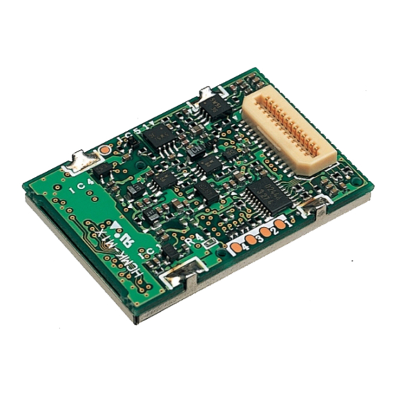
Page 8: Pc Board
VGS-1 PC BOARD ACCESSORY UNIT (X42-3250-60) Component side view (J72-0897-19) Ref. No. Address J72-0897-19 Component side Layer 1 Layer 2 Layer 3 Layer 4 Layer 5 Layer 6 Foil side ACCESSORY UNIT (X42-3250-60) Foil side view (J72-0897-19) Ref. No. Address... -
Page 9: Schematic Diagram
VGS-1 SCHEMATIC DIAGRAM... -
Page 10: Terminal Function
Leuvensesteenweg 248 J, 1800 Vilvoorde, Belgium KENWOOD ELECTRONICS FRANCE S.A. 13, Boulevard Ney, 75018 Paris, France KENWOOD ELECTRONICS U.K. LIMITED KENWOOD House, Dwight Road, Watford, Herts., WD18 9EB United Kingdom KENWOOD ELECTRONICS EUROPE B.V. Amsterdamseweg 37, 1422 AC Uithoorn, The Netherlands KENWOOD ELECTRONICS ITALIA S.p.A.
Need help?
Do you have a question about the VGS-1 and is the answer not in the manual?
Questions and answers