
Related Manuals for Z-World BL1800

Summary of Contents for Z-World BL1800
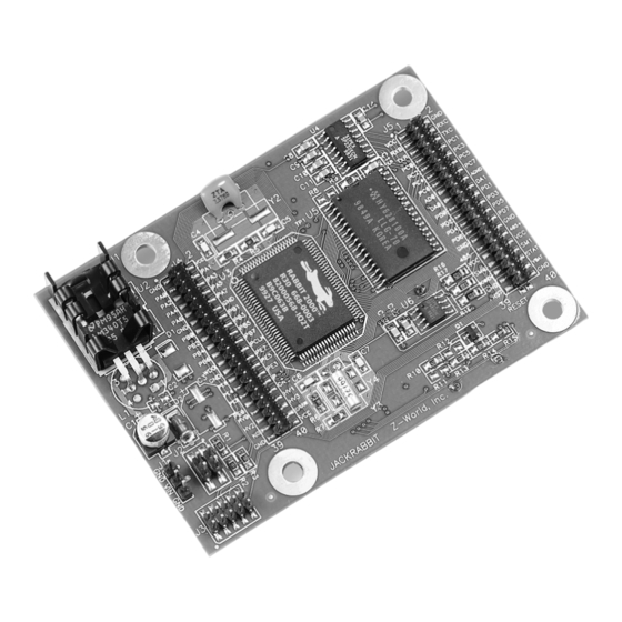
- Page 1 Jackrabbit (BL1800) C-Programmable Single-Board Computer User’s Manual 019–00067 • 030131–E...
- Page 2 Z-World reserves the right to make changes and improvements to its products without providing notice. Trademarks Rabbit 2000 is a trademark of Rabbit Semiconductor. Dynamic C is a registered trademark of Z-World Inc. Z-World, Inc. 2900 Spafford Street Davis, California 95616-6800...
-
Page 3: Table Of Contents
ABLE OF ONTENTS Chapter 1. Introduction 1.1 Features ..............................1 1.2 Development and Evaluation Tools......................2 1.3 How to Use This Manual ........................3 1.3.1 Additional Product Information ....................3 1.3.2 Online Documentation ........................3 1.4 CE Compliance .............................4 1.4.1 Design Guidelines .........................5 1.4.2 Interfacing the Jackrabbit to Other Devices..................5 Chapter 2. - Page 4 C.2 Batteries and External Battery Connections..................48 C.2.1 Battery Backup Circuit ......................49 C.2.2 Power to VRAM Switch ......................50 C.2.3 Reset Generator.......................... 50 C.3 Chip Select Circuit..........................51 Appendix D. Alternate Use of the Programming Port Notice to Users Index Schematics Jackrabbit (BL1800)
-
Page 5: Chapter 1. Introduction
1. I NTRODUCTION The Jackrabbit is a high-performance, C-programmable control- ler with a compact form factor. A Rabbit 2000™ microprocessor operating at 30 MHz provides fast data processing. 1.1 Features • 30 MHz clock • 24 CMOS-compatible I/O • 3 analog channels: 1 A/D input, 2 PWM D/A outputs •... -
Page 6: Development And Evaluation Tools
Jackrabbit. The Development Kit puts together the essentials you need to design an embedded microprocessor-based system rapidly and effi- ciently. See the Jackrabbit (BL1800) Getting Started Manual for complete information on the Development Kit. Jackrabbit (BL1800) -
Page 7: How To Use This Manual
Manual, which is also provided on the accompanying CD-ROM in both HTML and Adobe PDF format. We recommend that any users unfamiliar with Z-World products, or those who will be using the Prototyping Board for initial evaluation and development, begin with at least a read-through of the Getting Started manual. -
Page 8: Ce Compliance
CE qualified as they are sub-versions of the BL1800 single- board computer. Boards that are CE-compliant have the CE mark. NOTE: Earlier versions of the BL1800 sold before 2002 that do not have the CE mark are not CE-complaint. -
Page 9: Design Guidelines
Jackrabbit model BL1800, and must be turned on with at least one wait state in order for the BL1800 model to be CE-compliant. Section 2.7.3 provides further information about the spectrum spreader and its use, and includes information on how to add a wait state. - Page 10 Jackrabbit (BL1800)
-
Page 11: Chapter 2. Subsystems
Chapter 2 describes the principal subsystems and their use for the Jackrabbit. • Digital Inputs/Outputs • A/D Converter • D/A Converters • Serial Communication • Memory Figure 1 shows these Rabbit-based subsystems designed into the Jackrabbit. Digital BL1800 Inputs Programming Port Digital RS-232 15 MHz 32 kHz Outputs... -
Page 12: Jackrabbit Pinouts
485– 485+ IOBEN STAT VBAT +RAW /RST Figure 2. Pinout for Jackrabbit Headers J4 and J5 2.1.1 Headers Standard Jackrabbit models are equipped with two 2 × 20 IDC headers (J4 and J5) with a 2 mm pitch. Jackrabbit (BL1800) -
Page 13: Digital Inputs/Outputs
2.2 Digital Inputs/Outputs 2.2.1 Digital Inputs The Jackrabbit has six CMOS-level digital inputs, PB0–PB5, each of which is pulled up to +5 V as shown in Figure 3. The BL1820, which does not have RS-485, has one additional CMOS-level digital input, PC1. 47 kW Rabbit 2000 ™... -
Page 14: Digital Outputs
The K connection performs two functions. 1. K supplies power to the sinking/sourcing transistors used in the high-power circuits. 2. A diode-capacitor combination in the circuit “snubs” voltage transients when inductive loads such as relays and solenoids are driven. Jackrabbit (BL1800) - Page 15 Figure 5 are turned on. The maximum sourcing cur- rent is 100 mA (BL1810 and BL1820) or 500 mA (BL1800), and the maximum K is 30 V. This voltage limit on K arises because R51 and R52 at the base of Q28 can each dissipate 500 mW for a total of 1 W.
-
Page 16: Bidirectional I/O
/RST Figure 6. Changing HV3 to a Sinking Output 2.2.3 Bidirectional I/O The Jackrabbit has 14 CMOS-level bidirectional I/O: PA0–PA7, PD0, PD3, PD6–PD7, and PE4–PE5. The BL1820, which does not have RS-485, has one additional bidirectional I/O, PD5. Jackrabbit (BL1800) -
Page 17: A/D Converter
2.3 A/D Converter The analog-to-digital (A/D) converter, shown in Figure 7, compares the DA0 voltage to AD0, the voltage presented to the converter. DA0 therefore cannot be used for the digital- to-analog (D/A) converter when the A/D converter is being used. 51.1 kW 10 kW DA0 too low... - Page 18 The Jackrabbit is sold without this calibration sup- port. The algorithm provided to perform the conversion does a successive approximation search for the analog voltage. This takes an average of 150 ms, and a maximum of 165 ms, with a 14.7 MHz Jackrabbit. Jackrabbit (BL1800)
-
Page 19: D/A Converters
2.4 D/A Converters Two digital-to-analog (D/A) converter outputs, DA0 and DA1, are supplied on the Jack- rabbit. These are shown in Figure 8. The D/A converters have no reference voltage. Although they may be fairly accurate from one programmed voltage to the next, they do not have absolute accuracy. This is because Vcc can change ±5%, the PWM outputs might not achieve the full 0 V and 5 V rail out of the processor, and the gain resistors in the circuit have a 1% tolerance. -
Page 20: Da1
PWM for the D/A converters. The high limitation is simply the maximum voltage obtainable with the LM324 op amp used in the circuit. Anything outside the 12%–72% range gets output as Jackrabbit (BL1800) - Page 21 either a 0% or a 100% duty cycle. The duty cycle is programmed as the high-time count of 1024 total counts of the Rabbit 2000’s timer B. Thus, 256 counts would be 25% of 1024 counts, and corresponds to a 25% duty cycle. Table 2 lists typical DA1 voltages measured for various duty cycle values with a load larger than 1 MΩ.
-
Page 22: Da0
8 mV for a 3 V change in voltage). Seven time constants, 54 ms, will allow settling to within 99.91% (or to within about 3 mV for a 3 V change in voltage). The settling time is reduced somewhat by precharging capacitor C20 with pulse-width modulation from PD2. Jackrabbit (BL1800) - Page 23 The resolution of the DA0 output depends on the smallest increment of time to change the on/off time (the time between 5 V and 0 V). The Jackrabbit uses the Rabbit 2000’s Port D control registers to clock out the signal at a timer timeout. The timer used is timer B. Timer B has 10 bits of resolution so that the voltage can be varied in 1/1024 increments.
-
Page 24: Serial Communication
The half-duplex communication uses the Rabbit 2000’s PD5 pin to control the data enable on the communication line. The Jackrabbit can be used in an RS-485 multidrop network. Connect the RS-485+ to RS-485+ and RS-485– to RS-485– using single twisted-pair wires (nonstranded, tinned) as shown in Figure 9. Jackrabbit (BL1800) - Page 25 SRAM AGND Ground recommended Rabbit 2000 PCLK 485– 485+ IOBEN STAT +RAW VBAT RS-485 /RST RESET JACKRABBIT Z-World, Inc. SRAM AGND Rabbit 2000 PCLK 485– 485+ IOBEN STAT +RAW VBAT RS-485 /RST RESET JACKRABBIT Z-World, Inc. SRAM AGND Rabbit 2000 PCLK 485–...
-
Page 26: Programming Port
RS-485 /RST RESET JACKRABBIT Z-World, Inc. Figure 10. RS-485 Termination and Bias Resistors The load these bias and termination resistors present to the RS-485 transceiver (U6) limits the number of Jackrabbits in a multidrop network to one master and nine slaves, unless the bias and termination resistors are removed. -
Page 27: Memory
The Jackrabbit is also designed to accept 128K to 512K of flash EPROM packaged in a TSOP case. NOTE: Z-World recommends that any customer applications should not be constrained by the sector size of the flash memory since it may be necessary to change the sector size in the future. -
Page 28: Other Hardware
// Rabbit 2000: crystal <= 12.9024 MHz, // Rabbit 3000: crystal <= 26.7264 MHz, // or to 0 to always disable clock doubler to read as follows. #define CLOCK_DOUBLED 0 3. Save the change using File > Save Jackrabbit (BL1800) -
Page 29: Spectrum Spreader
Jackrabbit BL1800 models only, you will need at least one wait state for both the flash memory and the RAM. The strong spectrum-spreading setting is not needed for any Jackrabbit board. - Page 30 Jackrabbit (BL1800)
-
Page 31: Appendix A. Specifications
A. S PPENDIX PECIFICATIONS Appendix A provides the specifications for the Jackrabbit. User’s Manual... -
Page 32: Electrical And Mechanical Specifications
Table A-1 provides the pin 1 locations for the Jackrabbit headers. Table A-1. Jackrabbit Header Pin 1 Locations Pin 1 (x,y) Header Description Coordinates Power supply input (0.110, 0.700) External battery (0.415, 0.638) Programming port (0.145, 0.149) Jackrabbit subsystems (0.984, 2.023) Jackrabbit subsystems (3.184, 2.023) Jackrabbit (BL1800) - Page 33 Table A-2 lists the electrical, mechanical, and environmental specifications for the Jackrabbit boards. Table A-2. Jackrabbit Board Specifications Parameter BL1800 BL1810 BL1820 Microprocessor Rabbit 2000 @ 29.5 MHz Rabbit 2000 @ 14.7 MHz 256K 128K Flash EPROM (supports 128K–512K) (supports 128K–512K)
-
Page 34: Jumper Configurations
A.2 Jumper Configurations Figure A-2 shows the header and jumper locations used to configure the various Jackrabbit options. Top Side Bottom Side JACKRABBIT Z-World, Inc. Figure A-2. Location of Jackrabbit Configurable Positions Jackrabbit (BL1800) - Page 35 Table A-3 lists the configuration options. 0 Ω surface mount resistors are used for all the header positions. Table A-3. Jackrabbit Jumper Configurations Factory Header Description Pins Connected Default n.c. × SRAM Size 1–2 128K 2–3 512K × 1–2 128K/256K Flash Memory Size 2–3 512K ×...
-
Page 36: Conformal Coating
Any components in the conformally coated area may be replaced using standard soldering procedures for surface-mounted components. A new conformal coating should then be applied to offer continuing protection against the effects of moisture and contaminants. NOTE: For more information on conformal coatings, refer to Technical Note 303, Conformal Coatings. Jackrabbit (BL1800) -
Page 37: Use Of Rabbit 2000 Parallel Ports
RS-485 chip on BL1800 and BL1810 models), seven are inputs only (one of which is used by the RS-485 chip on BL1800 and BL1810 models), and five are outputs only (one of which is used by the RS-485 chip on BL1800 and BL1810 models), as shown in Figure A-4. - Page 38 Connected to RS-485 IC Input Rx output Connected to RS-232 IC Output Tx input Connected to RS-232 IC Input Rx output Connected to RS-232 IC Output Tx input Connected to RS-232 IC Input Rx output Output Connected to programming port Input Jackrabbit (BL1800)
- Page 39 Table A-4. Jackrabbit Pinout Configrations (continued) Rabbit 2000 Alternate Use Jackrabbit Use Factory Default Connected to control Connected to control Bitwise or parallel programmable I/O, can be driven or open- Connected to control ATXB output drain output Connected to RS-485 IC ARXB input data enable input ATXA output...
- Page 40 PCLK is as a peripheral clock or a peripheral clock ÷ 2, but PCLK can instead be used as a digital output. Similarly, IOBENB is an I/O buffer enable, but can instead be used as a digital output. STAT and WDO also have limited uses as digital outputs. Jackrabbit (BL1800)
-
Page 41: Appendix B. Prototyping Board
B. P PPENDIX ROTOTYPING OARD Appendix B describes the features and accessories of the Proto- typing Board, and explains the use of the Prototyping Board to demonstrate the Jackrabbit and to build prototypes of your own circuits. User’s Manual... -
Page 42: Mechanical Dimensions And Layout
B.1 Mechanical Dimensions and Layout Figure B-1 shows the mechanical dimensions and layout for the Jackrabbit Prototyping Board. Top Side Buzzer HV0 +RAW JACKRABBIT PROTOTYPING BOARD Z-World, Inc. 4.00 (102) Bottom Side Figure B-1. Jackrabbit Prototyping Board Jackrabbit (BL1800) -
Page 43: Using The Prototyping Board
Prototyping Board so that the initial setup is very straightforward. Once you have looked at the basic sample programs described in the Jackrabbit (BL1800) Getting Started Manual, solder the headers included in the bag of spare parts onto the Prototyping Board. -
Page 44: Demonstration Board
NOTE: If you do use the transformer supplied with the Development Kit for COIL(+), be aware that its voltage may be as high as 16 V at low current draws. This needs to be taken into consideration if you plan to use a 12 V relay in critical applications. Jackrabbit (BL1800) - Page 45 The thermistor has a nominal room-temperature resistance of about 10 kΩ, which drops to about 10 kW 6 kΩ at 40°C. Once you solder the thermistor onto Potentiometer Buzzer the RT1 pads (see Figure B-4) on the Prototyping Thermistor Board, the A/D readings on AD0 will change with HV0 +RAW temperature.
-
Page 46: Prototyping Board
PA6 to LED DS7 Header JP2 15–16 PA7 to LED DS8 Pins Description 17–18 PB2 to switch S1 1–2 PA0 to LED DS1 19–20 PB3 to switch S2 3–4 PA1 to LED DS2 21–22 PB4 to switch S3 Jackrabbit (BL1800) - Page 47 Once the LEDs, resistors, and switches are disconnected as described above, the user has a Jackrabbit board with connection points conveniently brought out to labeled points at headers J3 and J7 on the Prototyping Board. Small to medium circuits can be prototyped using point- to-point wiring with 20 to 30 AWG wire between the prototyping area and the holes at loca- tions J3 and J7.
- Page 48 Jackrabbit (BL1800)
-
Page 49: Appendix C. Power Management
C. P PPENDIX OWER ANAGEMENT C.1 Power Supplies Power is supplied to the Jackrabbit board from an external source through either header J1 or header J4. J1 is a 3-pin straight header with a pitch of 0.1". V is on pin 2 between ground on pins 1 and 3. - Page 50 105 mA when the programming cable is connected, and 95 mA when the programming cable is not connected. This means that DCIN can safely be from 7.5 V to 25 V. An addi- tional 50 mA is available for a daughterboard, but the voltage regulation would suffer slightly. Jackrabbit (BL1800)
- Page 51 8 V to 40 V. Figure C-3 shows typical power operating curves for both the linear regulator (BL1810 and BL1820) and the switching regulator (BL1800) for a nonloaded Jackrabbit operating at 14.7 MHz with the programming cable connected.
-
Page 52: Batteries And External Battery Connections
Figure C-4. External Battery Connections at Header J2 Alternatively, header J2 can be used to accommodate an external battery. In this case, be sure to cut out the soldered-in battery on the Jackrabbit to prevent discharging the external battery into a dead battery. Jackrabbit (BL1800) -
Page 53: Battery Backup Circuit
C.2.1 Battery Backup Circuit Figure C-5 shows the Jackrabbit battery backup circuitry. VRAM MMBT5088LT1 VBAT 4.3 MW 1.3 kW Figure C-5. Jackrabbit Battery Backup Circuit Resistor R12, shown in Figure C-5, is typically not stuffed on the Jackrabbit board. VRAM and Vcc are equal when power is supplied to the Jackrabbit. R13 prevents any cat- astrophic failure of Q1 from allowing unlimited current to enter the soldered-in battery. -
Page 54: Power To Vram Switch
Jackrabbit to reset. This input is available on headers J3 and J5, and also on pads directly below header J5. The two pads allow a screwdriver to be used to short the pads, forcing a reset. Jackrabbit (BL1800) -
Page 55: Chip Select Circuit
C.3 Chip Select Circuit Figure C-7 shows a schematic of the chip select circuit. VRAM /CSRAM /CS1 VRAM /RES Figure C-7. Chip Select Circuit The current drain on the battery in a battery-backed circuit must be kept at a minimum. When the Jackrabbit board is not powered, the battery keeps the SRAM memory contents and the real-time clock (RTC) going. - Page 56 R40. This small delay (about 160 µs) ensures that there is adequate time for the processor to write any last byte pending to the SRAM before the processor puts itself into a reset state. When coming out of reset, CS will be enabled very quickly because D20 conducts to charge capacitor C23. Jackrabbit (BL1800)
-
Page 57: Appendix D. Alternate Use Of The Programming Port
D. A PPENDIX LTERNATE SE OF THE ROGRAMMING Appendix D provides additional information for the program- ming port in association with the connectors DIAG PROG on the programming cable. The connector is used only PROG when the programming cable is attached to the programming connector (header J3) while a new application is being devel- oped. - Page 58 TXA to one of the SMODE pins and then test for the connection by raising PC6 (by configuring it as a general output bit) and reading the SMODE pin after the cold-boot mode has been disabled. The value of the SMODE pin is read from the SPCR register. Jackrabbit (BL1800)
-
Page 59: Notice To Users
Specifications are based on characterization of tested sample units rather than testing over temperature and voltage of each unit. Z-World products may qualify components to operate within a range of parameters that is different from the manufacturer’s recom- mended range. - Page 60 Jackrabbit (BL1800)
-
Page 61: Index
NDEX Prototyping Board ....37 adding additional headers . 39 A/D converter ....13, 14 features ........1 dimensions ......38 additional information flash memory ......23 how to disable demonstration Getting Started manual ..3 hardware ....... 42 online documentation ..3 installing relay .... - Page 62 Jackrabbit (BL1800)
-
Page 63: Schematics
CHEMATICS 090-0092 Jackrabbit Schematic www.zworld.com/documentation/schemat/090-0092.pdf 090-0088 Jackrabbit Prototyping Board Schematic www.zworld.com/documentation/schemat/090-0088.pdf 090-0128 Programming Cable Schematic www.zworld.com/documentation/schemat/090-0128.pdf The schematics included with the printed manual were the latest revisions available at the time the manual was last revised. The online versions of the manual contain links to the latest revised schematic on the Web site. - Page 64 Jackrabbit (BL1800)
Need help?
Do you have a question about the BL1800 and is the answer not in the manual?
Questions and answers