Motorola CP040 Detailed Service Manual
Hide thumbs
Also See for CP040:
- Basic user's manual (292 pages) ,
- Basic service manual (66 pages) ,
- Service information (46 pages)
Table of Contents
Advertisement
Quick Links
Advertisement
Table of Contents
Troubleshooting

Related Manuals for Motorola CP040


Summary of Contents for Motorola CP040
- Page 1 Commercial Series CP040 Radios Detailed Service Manual 6866549D19-B...
- Page 3 Commercial Series CP040 Radios Detailed Service Manual 6866549D19-B Contents Section 1 Service Maintainability Section 2 Power Distribution and Controller Service Information Section 3 VHF1 Service Information Section 4 VHF2 Service Information Section 5 UHF1 Service Information Section 6 UHF2 Service Information...
- Page 4 DOCUMENT HISTORY The following major changes have been implemented in this manual since the previous edition: Edition Description Date 6866549D19-O Initial edition Dec. 2003 6866549D19-A Added VHF 1 Band information. Oct. 2004 6866549D19-B - In the Service Maintainability Section: May 2008 Chapter 1, Updated Technical Support contact information.
- Page 5 Commercial Series CP040 Radios Service Maintainability Issue: May 2008...
- Page 6 Accordingly, any copyrighted Motorola computer programs contained in the Motorola products described in this manual may not be copied or reproduced in any manner without the express written permission of Motorola. Furthermore, the purchase of Motorola...
-
Page 7: Safety Information
Read this information before using the radio. PRODUCT SAFETY AND RF EXPOSURE FOR PORTABLE TWO-WAY RADIOS. This document provides information and instructions for the safe and efficient operation of Motorola Portable Two-Way Radios. The information provided in this document supersedes information contained in user guides published prior to February 2002. - Page 8 Compliance with RF Exposure Standards Your Motorola two-way radio is designed and tested to comply with a number of national and International standards and guidelines (listed below) for human exposure to radio frequency electromagnetic energy. This radio complies with the IEEE (FCC) and ICNIRP exposure limits for occupational/controlled RF exposure environments at operating duty factors of up to 50% talk- 50% listen and is authorized by the IEEE/ICNIRP for occupational use only.
- Page 9 - approved antennas, batteries and accessories may exceed IEEE/ICNIRP RF expo- sure guidelines. For a list of Motorola-approved antennas, batteries, and other accessories please see your dealer or local Motorola contact. Your nearest dealer can be found at the following web site: http://www.motorola.com/cgiss/emea/dealerlocator.html Additional Information For additional information on exposure requirements or other training information, visit http://www.motorola.com/rfhealth...
-
Page 10: Medical Devices
ELECTROMAGNETIC INTERFERENCE/COMPATIBILITY NOTE: Nearly every electronic device is susceptible to electromagnetic interference (EMI) if inadequately shielded, designed or otherwise configured for electromagnetic compatibility. Facilities To avoid electromagnetic interference and/or compatibility conflicts, turn off your radio in any facility where posted notices instruct you to do so. Hospitals or health care facilities may be using equipment that is sensitive to external RF energy. - Page 11 OPERATIONAL WARNINGS Vehicles with an air bag Refer to vehicle manufacturer's manual prior to installation of electronic equipment to avoid interference with air bag wiring. WARNING: Do not place a portable radio in the area over an air bag or in the air bag deployment area.
- Page 12 Warnings for Radios Approved as Intrinsically Safe Radios must ship from the Motorola manufacturing facility with the hazardous atmosphere capability and the intrinsic safety approval labelling (FM, UL, CSA, CENELEC or ATEX). Radios will not be upgraded to this capability and labeled once they have been shipped to the field.
- Page 13 The manual PN referenced on the Intrinsically Safe Approval Label identifies the approved Accessories and or options that can be used with that portable radio unit. Using a non Motorola intrinsically safe battery and or accessory with the Motorola approved radio unit will void the intrinsically safe approval of that radio unit.
- Page 14 THIS PAGE INTENTIONALLY LEFT BLANK...
-
Page 15: Table Of Contents
Table of Contents Chapter 1 INTRODUCTION 1.0 Scope of Manual ....................1-1 2.0 Warranty and Service Support................1-1 2.1 Warranty Period and Return Instructions ............1-1 2.2 After Warranty Period ..................1-1 2.3 European Radio Support Centre (ERSC)............1-2 2.4 Parts Identification and Ordering ..............1-2 2.5 EMEA Test Equipment Support..............1-2 2.6 Technical Support...................1-3 2.7 Related Documents ..................1-3... - Page 16 THIS PAGE INTENTIONALLY LEFT BLANK...
-
Page 17: Scope Of Manual
In instances where the product is covered under a "return for replacement" or "return for repair" warranty, a check of the product should be performed prior to shipping the unit back to Motorola. This is to ensure that the product has been correctly programmed or has not been subjected to damage outside the terms of the warranty. -
Page 18: European Radio Support Centre (Ersc)
Aftermarket and Accessory Division (AAD). If no part number is assigned, the part is not normally available from Motorola. If the part number is appended with an asterisk, the part is serviceable by Motorola Depot only. If a parts list is not included, this generally means that no user-serviceable parts are available for that kit or assembly. -
Page 19: Technical Support
Warranty and Service Support Technical Support Motorola Product Services is available to assist the dealer/distributors in resolving any malfunctions which may be encountered. North Europe - Stephen Woodrow Central and East Europe - Siggy Punzenberger Telephone: +44 (0) 1256 488 082... -
Page 20: Radio Model Information
INTRODUCTION Radio Model Information The model number and serial number are located on a label attached to the back of your radio. You can determine the RF output power, frequency band, protocols, and physical packages. The example below shows one mobile radio model number and its specific characteristics. Table 1-1 Radio Model Number (Example: MDH50KDC9AA2_N) Type of Model... -
Page 21: Introduction
Chapter 2 MAINTENANCE Introduction This chapter of the manual describes: ■ preventive maintenance ■ safe handling of CMOS devices ■ repair procedures and techniques Preventive Maintenance The radios do not require a scheduled preventive maintenance program; however, periodic visual inspection and cleaning is recommended. Inspection Check that the external surfaces of the radio are clean, and that all external controls and switches are functional. -
Page 22: Safe Handling Of Cmos And Ldmos
Equipment (WEEE) Directive 2002/96/EC and Restriction of Hazardous Subtances (ROHS) Directive 2002/95/EC). To maintain product compliance and reliability, use only the Motorola specified parts in this manual. For the identification of lead (Pb) free assemblies, all EPP products will carry the EPP Marking, shown below, on the printed circuit board (PCB). - Page 23 When damaged parts are replaced, identical parts should be used. If the identical replacement component is not locally available, check the parts list for the proper Motorola part number and order the component from the nearest Motorola Communications parts center listed in the “Piece Parts”...
- Page 24 MAINTENANCE Once solder wicks onto the new component, remove the heat from the solder. Heat the remaining pad with the soldering iron and apply solder until it wicks to the component. If necessary, touch up the first side. All solder joints should be smooth and shiny.
-
Page 25: Notes For All Schematics And Circuit Boards
(pF) or microfarads (µF), and inductance values are in nanohenries (nH) or microhenries (µH). DC voltages are measured from point indicated to chassis ground using a Motorola DC multimeter or equivalent. If the board has been removed from the chassis, the transmitter module mounting screws may be used for ground connection. - Page 26 MAINTENANCE Circuit Block Interconnection Legend: Name Description USWB+ Unswitched Battery Voltage (always on) 5 volts (regulated) 5 volts in RX mode only 5 volts in TX mode only RESET Low-line reset signal from U320 to uP D3_3V Digital 3.3 volts (regulated) Analog 3 volts (regulated) TX_ENA Transmit enable signal from uP to transmitter...
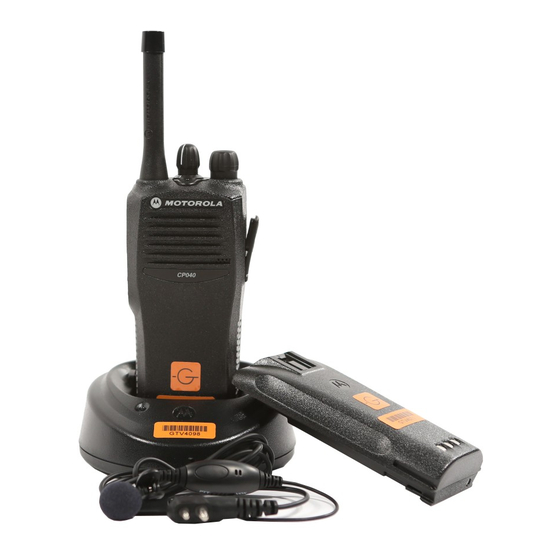
- Page 27 Speaker and Microphone Schematic MATES WITH J470 ON RADIO BOARD MATES WITH J491 ON RADIO BOARD Figure 1-2. Speaker and Microphone Schematic Speaker and Microphone Parts List Reference Motorola Part Description Designator 5080258E16 Microphone, electret 5005679X04 Speaker assembly with connector...
- Page 28 MAINTENANCE THIS PAGE INTENTIONALLY LEFT BLANK...
-
Page 29: Test Equipment
Table 3.2 lists the service aids recommended for working on the radio. While all of these items are available from Motorola, most are standard workshop equipment items, and any equivalent item capable of the same performance may be substituted for the item listed. - Page 30 SERVICE AIDS Table 3-2 Service Aids Motorola Part Description Application 5886564Z01 RF Adaptor Adapts radio’s antenna port to BNC cabling of test equipment. 0180305K08 Shop Battery Eliminator Interconnects radio to power supply. EPN4040 Wall-Mounted Power Supply Used to supply power to the RIB (UK).
- Page 31 Programming/Test Cable Table 3-2 Service Aids Motorola Part Description Application ChipMaster Nozzles: 6680332E83 PLCC-28* nozzle 6680332E82 PLCC-44* nozzle 6680332E94 PLCC-52 nozzle 6680332E96 PLCC-84 nozzle 6680334E67 QFP-160 nozzle Soldering and Un-soldering IC’s 6680333E46 SOL-18 nozzle 6680332E84 SOIC-20 nozzle 6680332E87 SOL-20J nozzle...
- Page 32 SERVICE AIDS 25 pin Male D Connector Components molded inside 2.5mm stereo and 3.5mm Orange 3.5mm Tip (Speaker +) Blue 3.5mm To Test Box Sleeve White 2.5mm Tip (Microphone) 1UF,16V 5% Spiral 2.5mm Yellow 2.5mm Center 25 pin Female D Connector To Test Box 3.5mm mono 2.5mm stereo...
- Page 33 Commercial Series CP040 Radios Power Distribution and Controller Service Information Issue: May 2008...
- Page 34 Accordingly, any copyrighted Motorola computer programs contained in the Motorola products described in this manual may not be copied or reproduced in any manner without the express written permission of Motorola. Furthermore, the purchase of Motorola...
- Page 35 Table of Contents Chapter 1 THEORY OF OPERATION 1.0 Overview......................1-1 2.0 Radio Power Distribution ..................1-1 3.0 Controller Circuits ....................1-3 3.1 General ......................1-3 3.2 Microprocessor Circuitry ................1-4 3.3 Audio Circuitry....................1-8 Chapter 2 TROUBLESHOOTING CHARTS 1.0 Troubleshooting Flow Chart for Board and IC Signals (includes Controller, DC Regulation and Audio) ..........
- Page 36 THIS PAGE INTENTIONALLY LEFT BLANK...
- Page 37 Chapter 1 THEORY OF OPERATION Overview This Chapter provides a detailed theory of operation for the controller circuits in the radio. The components of these circuits are contained on the Main Board. Refer to the RF sections of this manual for the component location details and the parts lists of the Controller Circuits. Radio Power Distribution Accessories 20 pin Connector...
- Page 38 THEORY OF OPERATION When the radio is turned on, SWB+ is present and is applied to: ■ transistor switch Q494 (pins 1 and 6) which turns on Q493 ■ RX audio power amplifier U490 ■ voltage divider R420/R421 and port PE0, a microprocessor A/D input which measures battery voltage and radio on/off status The output of FET switch Q493 is applied to the control pins of regulators U310, U320 and U330, turning them on.
-
Page 39: Controller Circuits
Controller Circuits Controller Circuits General The controller board is the central interface between the various subsystems of the radio. It provides the following functions: ■ interface with controls and indicators ■ serial bus control of major radio circuit blocks ■ encoding and/or decoding of selective signaling formats such as PL, DPL, MDC1200 and QuikCall II ■... - Page 40 THEORY OF OPERATION Microprocessor Circuitry The microprocessor circuitry includes microprocessor (U401) and associated EEPROM and Flash ROM memories. The following memory IC's are used: Table 1-2 Radio Memory Requirements Reference No. Description Type Size U402 Serial EEPROM AT25128 16K x 8 U403 Static RAM (not used)
- Page 41 PD5 (U401 pin 2) for the audio filter IC ■ port PH0 (U401 pin 47) for the synthesizer IC ■ port PH4 (U401 pin 43) for the option board/display enable (not used in CP040) ■ port PD6 (U401 pin 3) for the serial EEPROM 3.2.4...
- Page 42 THEORY OF OPERATION 3.2.6 Sensing of Externally-Connected Accessories Port PJ1 is used to detect the presence of externally connected accessories. Port PJ1 (U401 pin 72) is normally low, unless accessories (lapel speaker microphone, lightweight headset, etc.) are used with the radio. This port is used to detect an accessory PTT or auto sensing of a VOX accessory.
- Page 43 Controller Circuits 3.2.9 Microprocessor 7.3975 MHz Clock The 7.3975 MHz clock signal (uP_CLK) is provided from the ASFIC_CMP (U451 pin 28). Upon startup the 16.8MHz crystal provides the signal to the ASFIC_CMP, which sends out the uP_CLK at 3.8MHz until a steady-state condition is reached and the clock is increased to 7.3975MHz for the microprocessor.
- Page 44 (U510-1 and -2) for UHF models using low-side first injection. The gain of the buffer is 1.5 times or 3.5 dB. U480 and associated components are not used in CP040. Stage U480-1 is bypassed by jumper R487.
- Page 45 The Motorola RLN4460 Portable Test Set and PMKN4004 Programming Test Cable provide the proper interface between the radio's ungrounded audio output and ground-referenced test equipment.
- Page 46 1-10 THEORY OF OPERATION 3.3.6 Battery Charging Through Microphone Jack A wall-type charging power supply may be connected to the 2.5 mm microphone jack (part of accessory connector J451). The voltage present at the tip contact (pin 4) is applied to the center charging contact of the battery via diode D470.
- Page 47 Chapter 2 TROUBLESHOOTING TABLES Troubleshooting Tables for Board and IC Signals (includes Controller, DC Regulation and Audio) This section contains detailed troubleshooting tables. These tables should be used as a guide in determining the problem areas. They are not a substitute for knowledge of circuit operation and astute troubleshooting techniques.
- Page 48 TROUBLESHOOTING TABLES IC Designator Pin Function DC Voltage Comments (Condition) Inverter 1 input (25 kHz mode) BW Select Switch Inverter 2 output (25 kHz mode) Inverter 3 input (NU) Ground Inverter 3 output (NU) 4.96 Inverter 2 input 3.00 (25 kHz mode) Inverter 1 output 4.95 (25 kHz mode)
- Page 49 Troubleshooting Tables for Board and IC Signals (includes Controller, DC Regulation and Audio) IC Designator Pin Function DC Voltage Comments (Condition) U110 RF input (TX mode) RF Power Amp Vgg (gate bias) 2.65 (typ) (TX mode) (4.25V typ at VHF) 6.59 (TX mode) RF output...
- Page 50 TROUBLESHOOTING TABLES IC Designator Pin Function DC Voltage Comments (Condition) U201 Ref osc XTAL2 Freq Synthesizer Ref osc warp output 3.00 Superfilter cap 4.48 Superfilter base (NU) 3.76 Superfilter output 4.52 Superfilter input 4.96 Prescaler input 1.97 Prescaler ground Prescaler Vdd 2.99 Prescaler Vref (NU) 1.97...
- Page 51 Troubleshooting Tables for Board and IC Signals (includes Controller, DC Regulation and Audio) IC Designator Pin Function DC Voltage Comments (Condition) U251 Prescaler output 2.26 VCO / Buffer TX switch output (NU) 0.06 Vcc_BUFFERS 3.00 TX VCO emitter (RX mode) TX VCO base (RX mode) GND_LOGIC...
- Page 52 TROUBLESHOOTING TABLES IC Designator Pin Function DC Voltage Comments (Condition) U401 PD4_SCK serial clock input Microprocessor PD5_SS 3.23 ASFIC chip select PD6_VLIN 3.23 EEPROM chip select PG7_R_W 3.21 PG6_AS 3.23 PG0_XA13 3.23 PB7_ADDR15 0.026 PB6_ADDR14 0.028 PB3_ADDR11 3.06 PB1_ADDR9 3.05 PB2_ADDR10 0.16 3.23...
- Page 53 Troubleshooting Tables for Board and IC Signals (includes Controller, DC Regulation and Audio) IC Designator Pin Function DC Voltage Comments (Condition) U401 PH7_CSPROG 3.05 Microprocessor VDDL 3.23 VSSL PH6_CSGP2 3.23 PH5_CSGP1 3.23 PH4_CSIO PH3_PW4 3.21 On/off control output PH2_PW3 PH1_PW2 3.00 PH0_PW1 3.23...
- Page 54 TROUBLESHOOTING TABLES IC Designator Pin Function DC Voltage Comments (Condition) U401 3.23 Microprocessor 3.23 Bottom option button 3.23 Top option button PA0_IC3 PA1_IC2 1.57 PA2_IC1 3.00 PA3_IC4_OC5_OC1 3.00 PA4_OC4_OC1 Squelch detect input PA5_OC3_OC1 Channel activity input PA6_OC2_OC1 PA7_PA1_OC1 VSSR VDDR 3.23 ECLK (NU) 1.60...
- Page 55 Troubleshooting Tables for Board and IC Signals (includes Controller, DC Regulation and Audio) IC Designator Pin Function DC Voltage Comments (Condition) U404 3.06 Flash ROM 3.08 3.05 0.13 0.31 3.17 EN_WE 3.21 From U401-4 3.23 RESET 3.20 U404 3.17 Flash ROM 0.30 0.22 3.03...
- Page 56 2-10 TROUBLESHOOTING TABLES IC Designator Pin Function DC Voltage Comments (Condition) U451 VDD for analog circuits 3.00 ASFIC_CMP DISC audio input 1.34 From U510 Ground for analog circuits DACU output DACR output DACG output 2.38 (typ) Power set (TX mode) VOX peak detector output 2.91 PLCAP for DC integrator...
- Page 57 Troubleshooting Tables for Board and IC Signals (includes Controller, DC Regulation and Audio) 2-11 IC Designator Pin Function DC Voltage Comments (Condition) U451 GCB5 general purpose output ASFIC_CMP RX audio send to option 1.48 Modulation output 1.50 To U201-10 RX audio out to power amp 1.51 Flat TX audio return from option 0.20...
- Page 58 2-12 TROUBLESHOOTING TABLES THIS PAGE INTENTIONALLY LEFT BLANK...
- Page 59 Chapter 3 CONTROLLER SCHEMATICS Allocation of PCBs and Schematic Diagrams The Controller circuits are contained on the printed circuit board (PCB) containing the RF circuits. This Chapter shows the schematics for the Controller circuits only, refer to the relevant RF section for details of the related RF circuits, the PCB component layouts and the complete radio parts lists.
- Page 60 CONTROLLER SCHEMATICS PCBs : 8416847H01-A UHF3 (EPP) 8416847H02-B UHF3 (EPP) SCHEMATICS Controller Interconnect Schematic Page 3-17 Microprocessor Circuit Schematic Page 3-18 Audio Circuit Schematic (UHF3) Page 3-19 DC Regulation Schematic (UHF3) Page 3-20...
- Page 61 Controller Schematics Controller Schematics SW_B+ OPT_MIC OPT_TX_AUD_FLAT_RETURN OPT_TX_AUD_RETURN PWR_SET PWR_SET OPT_TX_AUD_SEND CNTL_PWR_SET DEMOD OPT_RX_AUD_SEND_DETECTOR DEMOD CNTL_DEMOD OPT_RX_AUD_SEND_UNMUTED AUDIO BW_SEL BW_SEL OPT_RX_AUD_RETURN CNTL_BW_SEL MOD_OUT MOD_OUT CNTL_MOD_OUT VS_AUDIO_SEL 16_8_MHZ 16_8_MHZ VS_GAIN_SEL CNTL_16_8_MHZ E500 BK1005HM471 C500 C501 1000pF D3_3V SW_B+ SPI_CLK CNTL_SPI_CLK SPI_DATA_OUT CNTL_SPI_DATA_OUT R502 SYNTH_CS...
- Page 62 Controller Schematics D3_3V R410 R416 R417 C418 0.1uF TP405 R411 D3_3V R419 4.7K TP402 C419 D3_3V 1000pF Q410 R412 C410 C411 C413 C412 100K 0.1uF 0.1uF 10uF TP401 1000pF LSIO HOLD CH_ACT U402 X25128-2.7 EEPROM SQ_DET HSIO SPI_DATA_IN OPT_DATA_READY SPI_DATA_OUT uP_CLK SPI_CLK D3_3V...
- Page 63 Controller Schematics 150 mV RMS (25 kHz) (Rx) R523 75 mv RMS (12.5 kHz) (Rx) R516 R522 100K C512 C514 6.8pF 16pF R512 R514 Q520-2 150K 100K IMX1 5V_A R511 100K Q520-1 DEMOD R513 R515 IMX1 C518 0.1uF OPT_RX_AUD_SEND_DETECTOR 5V_A C460 0.1uF R470...
- Page 64 Controller Schematics R516 R523 Audio C512 C514 R522 Q520 6.8pF 16pF IMX1 100K R512 150K R514 5V_A 100K U510-1 LM2904 Q520 IMX1 R511 C518 R513 DEMOD C460 R515 VR471 100K 0.1uF R470 OPT_RX_AUD_SEND_DETECTO R 5V_A U510-2 0.1uF C511 C513 2.2K LM2904 OPT_RX_AUD_RETURN 220pF...
- Page 65 Controller Schematics USWB+ U310 TK71750S 7.5 V VOUT CTRL F301 DATA BYPASS J301 C301 C313 C304 C311 C303 C310 C312 390pF D301 .01uF VR301 .01uF .01uF .018uF 33uF 10uF MMBZ5250B D3_3V BATT_CHARGE 5 V (Rx) Q311 0 V (Tx) R310 C314 1200pF 100K...
- Page 66 Controller Schematics DC Regulation USWB+ U310 TK71750S VR301 F301 J301 MMBZ5250B 1 VIN VOUT 4 CTRL D301 C304 C301 C303 BYPASS C311 C312 C313 DATA 47pF 33uF .01uF .018uF 10uF .01uF Q311 C310 .01uF D3_3V BATT_CHARGE VR302 C314 R310 MMBZ5250B 100K C302 C305...
- Page 67 Controller Schematics SW_B+ OPT_MIC OPT_TX_AUD_FLAT_RETURN OPT_TX_AUD_RETURN PWR_SET PWR_SET OPT_TX_AUD_SEND CNTL_PWR_SET OPT_RX_AUD_SEND_DETECTOR DEMOD DEMOD CNTL_DEMOD OPT_RX_AUD_SEND_UNMUTED AUDIO BW_SEL BW_SEL OPT_RX_AUD_RETURN CNTL_BW_SEL MOD_OUT MOD_OUT CNTL_MOD_OUT VS_AUDIO_SEL 16_8_MHZ 16_8_MHZ VS_GAIN_SEL CNTL_16_8_MHZ E500 BK1005HM471 C500 C501 1000pF D3_3V SW_B+ SPI_CLK CNTL_SPI_CLK SPI_DATA_OUT CNTL_SPI_DATA_OUT R502 SYNTH_CS CNTL_SYNTH_CS C503...
- Page 68 3-10 Controller Schematics D3_3V R410 R416 R417 C418 0.1uF TP405 R411 D3_3V R419 4.7K TP402 C419 D3_3V 1000pF Q410 R412 C410 C411 C413 C412 100K 0.1uF 0.1uF 10uF TP401 1000pF LSIO HOLD CH_ACT U402 X25128-2.7 EEPROM SQ_DET HSIO SPI_DATA_IN OPT_DATA_READY SPI_DATA_OUT uP_CLK SPI_CLK...
- Page 69 Controller Schematics 3-11 150 mV RMS (25 kHz) (Rx) R523 75 mv RMS (12.5 kHz) (Rx) R516 R522 100K C512 C514 6.8pF 16pF R512 R514 Q520-2 150K 100K IMX1 5V_A R511 100K Q520-1 DEMOD R513 IMX1 R515 C518 0.1uF OPT_RX_AUD_SEND_DETECTOR 5V_A C460 0.1uF...
- Page 70 3-12 Controller Schematics USWB+ U310 TK71750S 7.5 V VOUT CTRL F301 DATA BYPASS C301 J301 C313 C303 C304 C310 C311 C312 390pF D301 .01uF VR301 .01uF .01uF .018uF 33uF 10uF MMBZ5250B D3_3V BATT_CHARGE 5 V (Rx) Q311 0 V (Tx) R310 C314 1200pF...
- Page 71 Controller Schematics 3-13 SW_B+ OPT_MIC OPT_TX_AUD_FLAT_RETURN OPT_TX_AUD_RETURN PWR_SET PWR_SET OPT_TX_AUD_SEND CNTL_PWR_SET DEMOD OPT_RX_AUD_SEND_DETECTOR DEMOD CNTL_DEMOD OPT_RX_AUD_SEND_UNMUTED AUDIO BW_SEL BW_SEL OPT_RX_AUD_RETURN CNTL_BW_SEL MOD_OUT MOD_OUT CNTL_MOD_OUT VS_AUDIO_SEL 16_8_MHZ 16_8_MHZ VS_GAIN_SEL CNTL_16_8_MHZ E500 BK1005HM471 C500 C501 1000pF D3_3V SW_B+ SPI_CLK CNTL_SPI_CLK SPI_DATA_OUT CNTL_SPI_DATA_OUT R502 SYNTH_CS C503...
- Page 72 3-14 Controller Schematics D3_3V R410 R416 R417 C418 0.1uF $O,$V TP405 R411 D3_3V R419 4.7K TP402 C419 D3_3V 1000pF Q410 R412 C411 C413 C410 C412 100K 10uF 0.1uF 0.1uF TP401 1000pF LSIO HOLD CH_ACT U402 X25128-2.7 EEPROM SQ_DET HSIO SPI_DATA_IN OPT_DATA_READY SPI_DATA_OUT uP_CLK...
- Page 73 Controller Schematics 3-15 UHF1/2 (403-440MHz and 438-470MHz) Audio Circuitry Schematic Diagram (PCB 8416205H02-C/-D)
- Page 74 3-16 Controller Schematics USWB+ U310 TK71750S 7.5 V VOUT CTRL F301 DATA BYPASS C301 J301 C313 C304 C310 C311 C303 C312 390pF D301 .01uF .01uF .018uF VR301 33uF .01uF 10uF MMBZ5250B D3_3V 5 V (Rx) BATT_CHARGE 0 V (Tx) Q311 C314 R310 1200pF...
- Page 75 Controller Schematics 3-17 SW_B+ OPT_MIC OPT_TX_AUD_FLAT_RETURN OPT_TX_AUD_RETURN PWR_SET PWR_SET OPT_TX_AUD_SEND CNTL_PWR_SET DEMOD OPT_RX_AUD_SEND_DETECTOR DEMOD CNTL_DEMOD OPT_RX_AUD_SEND_UNMUTED AUDIO BW_SEL BW_SEL OPT_RX_AUD_RETURN CNTL_BW_SEL MOD_OUT MOD_OUT CNTL_MOD_OUT VS_AUDIO_SEL 16_8_MHZ 16_8_MHZ VS_GAIN_SEL CNTL_16_8_MHZ E500 BK1005HM471 C500 C501 1000pF D3_3V SW_B+ SPI_CLK CNTL_SPI_CLK SPI_DATA_OUT CNTL_SPI_DATA_OUT R502 SYNTH_CS C503...
- Page 76 3-18 Controller Schematics R410 R416 R417 C418 0.1uF D3_3 $O,$V TP405 R401 300K D3_3V D3_3V R419 4.7K C425 Q410 C411 C413 R408 C410 C412 100K 10uF 0.1uF 0.1uF 1000pF TP401 U425 LMC7101BI HOLD U402 X25128-2.7 EEPROM D3_3V R400 R418 100K C414 C417 0.1uF...
- Page 77 Controller Schematics 3-19 R523 100K R516 R522 100K C512 C514 6.8pF 16pF R512 R514 Q520-2 150K 100K IMX1 5V_A R511 100K Q520-1 DEMOD R513 IMX1 R515 C518 0.1uF OPT_RX_AUD_SEND_DETECTOR 5V_A C460 0.1uF R470 U510-1 OPT_RX_AUD_RETURN 2.2K LM2904 U510-2 VR471 C511 C513 LM2904 3V_A...
- Page 78 3-20 Controller Schematics USWB+ U310 TK71750S VOUT CTRL J301 F301 DATA BYPASS C301 C313 C304 C310 C311 C303 C312 390pF D301 .01uF .01uF .018uF VR301 33uF .01uF 10uF MMBZ5250B D3_3V BATT_CHARGE Q311 C314 R310 1200pF 100K C302 C305 C306 390pF VR302 R313 R312...
- Page 79 Commercial Series CP040 Radios VHF1 (136-162MHz) Service Information Issue: May 2008...
- Page 80 Accordingly, any copyrighted Motorola computer programs contained in the Motorola products described in this manual may not be copied or reproduced in any manner without the express written permission of Motorola. Furthermore, the purchase of Motorola...
- Page 81 Table of Contents Chapter 1 THEORY OF OPERATION 1.0 Introduction ......................1-1 2.0 VHF1 (136-162MHz) Receiver................1-1 2.1 Receiver Front-End ..................1-2 2.2 Receiver Back-End..................1-3 3.0 VHF1 (136-162MHz) Transmitter.................1-4 3.1 Transmitter Power Amplifier ................1-4 3.2 Antenna Switch....................1-4 3.3 Harmonic Filter ....................1-5 3.4 Antenna Matching Network ................1-5 3.5 Power Control....................1-5 4.0 VHF1 (136-162MHz) Frequency Generation Circuitry.........1-6 4.1 Fractional-N Synthesizer ................1-7...
- Page 82 THIS PAGE INTENTIONALLY LEFT BLANK...
- Page 83 Chapter 1 THEORY OF OPERATION Introduction This Chapter provides a detailed theory of operation for the VHF circuits in the radio. Schematic diagrams and board layout diagrams are included in Chapter 4 in this Section of the manual. VHF1 (136-162MHz) Receiver The VHF receiver covers the range of 136-162 MHz and provides switchable IF bandwidth for use with 20/25 kHz or 12.5 kHz channel spacing systems.
- Page 84 THEORY OF OPERATION Receiver Front End Incoming RF signals from the antenna are first routed through the harmonic filter and antenna switch, part of the transmitter circuitry, before being applied to the receiver front end. The receiver front end consists of a preselector filter, RF amplifier, an interstage filter, and a double-balanced first mixer.
- Page 85 VHF1 (136-162MHz) Receiver Receiver Back End The receiver back end is a dual conversion design. High IF selectivity is provided by FL51, a 4-pole fundamental mode 44.85 MHz crystal filter with a minimum 3 dB bandwidth of + 6.7 kHz, a maximum 20 dB bandwidth of ±12.5 kHz, and a maximum insertion loss of 3.5 dB.
-
Page 86: Vhf Transmitter
THEORY OF OPERATION VHF Transmitter The VHF transmitter covers the range of 136-162 MHz. Depending on model, the output power of the transmitter is either switchable on a per-channel basis between high power (5 watts) and low power (1 watt), or is factory preset to 2 watts. The transmitter is divided into four major blocks as shown in Figure 2-2. - Page 87 VHF Transmitter Harmonic Filter The harmonic filter consists of components C130-C136 and L130-L132. The harmonic filter is a seven-pole elliptical low-pass configuration, optimized for low insertion loss, with a 3 dB frequency of approximately 180 MHz and typically less than 0.8 dB insertion loss in the passband. Antenna Matching Network The harmonic filter presents a 50Ω...
- Page 88 THEORY OF OPERATION VHF Frequency Generation Circuitry The frequency generation system, shown in Figure 2-3, is composed of two circuit blocks, the Fractional-N synthesizer IC U201, the VCO/Buffer IC U251, and associated circuitry. Figure 2-4 shows the peripheral interconnect and support circuitry used in the synthesizer block, and Figure 2-5 details the internal circuitry of the VCOBIC and its interconnections to the surrounding components.
- Page 89 VHF Frequency Generation Circuitry Fractional-N Synthesizer The Fractional-N synthesizer, shown in Figure 2-4, uses a 16.8 MHz crystal (Y201) to provide the reference frequency for the system. External components C201-C203, R202 and D201 are also part of the temperature-compensated oscillator circuit. The dc voltage applied to varactor D201 from U201 pin 25 is determined by a temperature-compensation algorithm within U201, and is specific to each crystal Y201, based on a unique code assigned to the crystal that identifies its temperature characteristics.
- Page 90 THEORY OF OPERATION Voltage Controlled Oscillator (VCO) The VCOBIC (U251), shown in Figure 2-5, in conjunction with the Fractional-N synthesizer (U201) generates RF in both the receive and the transmit modes of operation. The TRB line (U251 pin 19) determines which oscillator and buffer are enabled. A sample of the RF signal from the enabled oscillator is routed from U251 pin 12 through a low pass filter, to the prescaler input of the synthesizer IC (U201 pin 32).
- Page 91 Chapter 2 TROUBLESHOOTING TABLES This section contains detailed troubleshooting tables. These tables should be used as a guide in determining the problem areas. They are not a substitute for knowledge of circuit operation and astute troubleshooting techniques. It is advisable to refer to the related detailed circuit descriptions in the theory of operation sections prior to troubleshooting a radio.
- Page 92 TROUBLESHOOTING TABLES Symptom Possible Causes Procedure Corrective Action No Audio 1. Synthesizer out of lock Verify U201-4 is at 3V dc. Troubleshoot synthesizer/VCO circuits. 2. Defective IFIC Verify audio is present at U51-8. Check Q70, Y70, U51. 3. RX audio buffer fault Verify audio is present at U451-2.
- Page 93 Troubleshooting Table for Synthesizer Troubleshooting Table for Synthesizer Symptom Possible Causes Procedure Corrective Action Synthesizer Out of 1. VCO fault Verify oscillator is working, check RF Check VCO tank components Lock (RX mode level at U251-10 per schematic. connected to U251-5 and 6. only) Check dc voltages at U251 pin 2 Check for shorts/opens, replace...
- Page 94 TROUBLESHOOTING TABLES Troubleshooting Table for Transmitter Symptom Possible Causes Procedure Corrective Action No Transmit (no 1. PTT switch defective. Verify U401-71 goes low when PTT Replace PTT switch S441. TX LED indication) is pressed. 2. EXT MIC PTT fault Verify U401-72 goes low when J471- Check/replace Q470, L471 etc.
- Page 95 Troubleshooting Table for Transmitter Symptom Possible Causes Procedure Corrective Action Poor TX range, 1. RF test jack defective Verify continuity of J140 pins 3 and 4 Replace J140. conducted power in RX mode only. 2. Antenna matching net- Visually inspect components C140- Repair/replace if necessary.
- Page 96 TROUBLESHOOTING TABLES Troubleshooting Table for Board and IC Signals IC Designator Pin Function DC Voltage Comments (Condition) RF input 44.85 MHz 1.20 IFIC RF input decoupling 1.20 2nd LO osc output 4.02 2nd LO osc input 4.60 RSSI output 0.74 (no received signal) 4.70 Audio feedback...
- Page 97 Troubleshooting Table for Board and IC Signals IC Designator Pin Function DC Voltage Comments (Condition) U110 RF input (TX mode) RF Power Amp Vgg (gate bias) 4.25V (typ) (TX mode) 6.59 (TX mode) RF output Do not measure Ground U150 Unit 1 output 5.8V (typ) (TX mode)
- Page 98 TROUBLESHOOTING TABLES IC Designator Pin Function DC Voltage Comments (Condition) U201 Ref osc XTAL2 Freq Synthesizer Ref osc warp output 3.00 Superfilter cap 4.48 Superfilter base (NU) 3.76 Superfilter output 4.52 Superfilter input 4.96 Prescaler input 1.97 Prescaler ground Prescaler Vdd 2.99 Prescaler Vref (NU) 1.97...
- Page 99 Troubleshooting Table for Board and IC Signals IC Designator Pin Function DC Voltage Comments (Condition) U251 Prescaler output 2.26 VCO / Buffer TX switch output (NU) 0.06 Vcc_BUFFERS 3.00 TX VCO emitter (RX mode) TX VCO base (RX mode) GND_LOGIC Vcc_LOGIC 3.00 TRB input...
- Page 100 2-10 TROUBLESHOOTING TABLES IC Designator Pin Function DC Voltage Comments (Condition) U401 PB1_ADDR9 3.05 Microprocessor PB2_ADDR10 0.16 3.23 PBO_ADDR8 3.05 PB5_ADDR13 0.13 PG1_XA14 0.20 PG4_XA17 3.17 PG5_XA18 PG3_XA16 3.21 PG2_XA15 0.30 PB4_ADDR12 0.22 PF7_ADDR7 3.03 PF6_ADDR6 3.08 PF5_ADDR5 3.06 PF4_ADDR4 0.16 PF3_ADDR3 0.26...
- Page 101 Troubleshooting Table for Board and IC Signals 2-11 IC Designator Pin Function DC Voltage Comments (Condition) U401 PH1_PW2 3.00 Microprocessor PH0_PW1 3.23 Synth chip select XIRQ 3.00 1.48 RX enable 0.01 TX enable 3.23 Green LED enable Red LED enable 2.98 Lock detect from U201-4 MODB_VSTBY...
- Page 102 2-12 TROUBLESHOOTING TABLES IC Designator Pin Function DC Voltage Comments (Condition) U401 PA3_IC4_OC5_OC1 3.00 Microprocessor PA4_OC4_OC1 Squelch detect input PA5_OC3_OC1 Channel activity input PA6_OC2_OC1 PA7_PA1_OC1 VSSR VDDR 3.23 ECLK (NU) 1.60 EXTAL 1.70 Clock from U451-28 XTAL 1.40 Not used VDDSYN XFC (NU) RESET...
- Page 103 Troubleshooting Table for Board and IC Signals 2-13 IC Designator Pin Function DC Voltage Comments (Condition) U404 3.17 Flash ROM 0.30 0.22 3.03 3.08 3.06 0.24 3.08 3.05 3.05 0.69 0.94 1.08 0.78 0.59 0.66 0.67 0.75 EN_CE 3.01 From U401-38 0.16 EN_OE From U401-86...
- Page 104 2-14 TROUBLESHOOTING TABLES IC Designator Pin Function DC Voltage Comments (Condition) U451 GCB1 general purpose output ASFIC_CMP GCB0 general purpose output 3.00 BW select (25 kHz mode) Squelch channel activity output To U401-84 Squelch detect digital output To U401-83 PL/low speed data I/O 1.50 High speed data I/O 3.00...
- Page 105 Troubleshooting Table for Board and IC Signals 2-15 IC Designator Pin Function DC Voltage Comments (Condition) U480 Unit 1 output 2.48 Dual Opamp Unit 1 (-) input 2.48 Unit 1 (+) input 2.46 Ground Unit 2 (+) input 0.28 Unit 2 (-) input 0.29 Unit 2 output 4.96...
- Page 106 2-16 TROUBLESHOOTING TABLES...
- Page 107 Chapter 3 VHF1 PCB/SCHEMATICS/PARTS LISTS Allocation of Schematics and Circuit Boards VHF1 (136-162MHz) The VHF circuits are contained on the printed circuit board (PCB) which also contains the Controller circuits. This Chapter shows the schematics for the VHF circuits, the Controller circuits are contained in Section 2 of this manual.
- Page 108 LAYER 6 (L6) SIDE 2 Speaker and Microphone Schematic MATES WITH J470 ON RADIO BOARD MATES WITH J491 ON RADIO BOARD 1.3.1 Speaker and Microphone Parts List Reference Motorola Part Description Designator 5080258E16 Microphone, electret 5005679X04 Speaker assembly with connector...
- Page 109 VHF1 PCB 8486769Z02-A Schematic Diagrams VHF1 PCB 8486769Z02-A Schematic Diagrams D301 R406 R480 C488 C465 C458 C454 U425 Q425 R408 R405 D425 Q426 C480 S444 R401 C513 R403 J471 R473 R470 R409 U451 FL54 R496 C470 L265 L255 C257 D262 C473 R481 R472...
- Page 110 VHF1 PCB 8486769Z02-A Schematic Diagrams SH200 C140 C206 R206 C52 C53 L120 C220 R416 C417 R411 U151 L130 L132 C222 R121 R434 R502 R433 L140 C221 FL51 R432 C131 C135 C223 R150 R501 R120 C224 C157 R151 D121 R154 R227 C228 C152 C123...
- Page 111 VHF1 PCB 8486769Z02-A Schematic Diagrams USWB+ USWB+ TX_ENA TX_ENA PWR_SET TX_VHF_R2 PWR_SET DEMOD DEMOD RX_BE RX_FE_VHF_R2 BW_SEL BW_SEL IF_IN IF_OUT RX_IN RX_OUT RSSI RSSI CONTROLLER MOD_OUT MOD_IN PRESC PRESC 16_8_MHZ 16_8_MHZ RX_INJ V_STEER V_STEER SYNTH_CS SYNTH_CS SYNTH_VHF_R2 VCO_VHF_R2 V_SF V_SF SPI_CLK SPI_CLK VCO_MOD...
- Page 112 VHF1 PCB 8486769Z02-A Schematic Diagrams 5.0V (Rx) 0V (Tx) FE_5R 6.8K 1000pF 3.95V (Rx) UMT1 500mV (RF) 3.95V (Rx) IF_OUT FE_IF_OUT 680nH 3.38V (Rx) 1000pF 2.0V (Rx) 100nH 1000pF 0.1uF 6.8K 3.9V (Rx) 150nH 82pF 700mV (RF) 68nH 10pF 30pF 68nH 24pF 27pF...
- Page 113 VHF1 PCB 8486769Z02-A Schematic Diagrams RX Back End (Overtone) U52-1 FL53 TC7W04F CFWC455E 0.1uF OUT 2 U52-2 100K TC7W04F IF_BAND_SEL 5V for 25kHz BW_SE L 0V for 12.5kHz 0.1uF FL54 CFWC455G 1 IN U52-3 47pF 3.3K SH50 SH52 TC7W04F SHIELD SHIELD U52-4 2.4K...
- Page 114 VHF1 PCB 8486769Z02-A Schematic Diagrams V_SF FN_V_SF 4.5V C231 C232 C233 1000pF 0.1uF 4.7uF R230 R247 200K 270K LOCK FN_LOCK LOCK: 3V UNLOCK: 0V WARP C204 INDMULT 470pF SFOUT ADAPTSW CCOMP LOCK C241 REFSEL IADAPT 1200pF V_STEER IOUT PRESC PREIN R245 FN_V_STEER 3.0V to 8.0V...
- Page 115 VHF1 PCB 8486769Z02-A Schematic Diagrams V_SF V_SF L270 4.5V VCO_VSF R273 560nH C292 1200pF C270 C274 C285 1200pF R270 0.1uF 0.1uF VCO_3V C272 0.1uF L282 R284 L292 47nH R272 68nH 9.1K C273 R271 8.2K .01uF 1200 mV (RF) R274 L271 C271 TX_INJ TX_IADJ...
- Page 116 VHF1 PCB 8486769Z02-A Schematic Diagrams 3-10 7.5 V USWB+ PA_USWB+ C170 0.1uF 0 V (Rx) 7.4 V (Rx) R171 0.15 V (Tx) Q171 TX_ENA MMBT3904 Q170 6.8K PA_TX_ENA EMB10 1.8V (Tx) R524 0 V (Rx) 7.25 V (Tx) C172 1500pF 0 V (Rx) C157 0.1uF...
- Page 117 VHF1 PCB 8486769Z02-A Schematic Diagrams 3-11 SW_B+ OPT_MIC OPT_TX_AUD_FLAT_RETURN OPT_TX_AUD_RETURN PWR_SET PWR_SET OPT_TX_AUD_SEND CNTL_PWR_SET DEMOD OPT_RX_AUD_SEND_DETECTOR DEMOD CNTL_DEMOD OPT_RX_AUD_SEND_UNMUTED AUDIO BW_SEL BW_SEL OPT_RX_AUD_RETURN CNTL_BW_SEL MOD_OUT MOD_OUT CNTL_MOD_OUT VS_AUDIO_SEL 16_8_MHZ 16_8_MHZ VS_GAIN_SEL CNTL_16_8_MHZ E500 BK1005HM471 C500 C501 1000pF D3_3V SW_B+ SPI_CLK CNTL_SPI_CLK SPI_DATA_OUT CNTL_SPI_DATA_OUT...
- Page 118 VHF1 PCB 8486769Z02-A Schematic Diagrams 3-12 D3_3V R410 R416 R417 C418 0.1uF TP405 R411 D3_3V R419 4.7K TP402 C419 D3_3V 1000pF Q410 R412 C411 C410 C413 C412 100K 0.1uF 0.1uF 10uF 1000pF TP401 LSIO HOLD CH_ACT U402 X25128-2.7 EEPROM SQ_DET HSIO SPI_DATA_IN OPT_DATA_READY...
- Page 119 VHF1 PCB 8486769Z02-A Schematic Diagrams 3-13 VHF1 (136-162 MHz) Audio Circuitry Schematic Diagram (8486769Z02-A)
- Page 120 VHF1 PCB 8486769Z02-A Schematic Diagrams 3-14 USWB+ U310 TK71750S 7.5 V VOUT CTRL F301 DATA BYPASS J301 C301 C313 C304 C310 C311 C303 C312 390pF D301 .01uF .01uF .018uF VR301 33uF .01uF 10uF MMBZ5250B D3_3V BATT_CHARGE 5 V (Rx) Q311 0 V (Tx) C314 R310...
- Page 121 VHF1 PCB 8486769Z02-A Parts List 3-15 VHF1 PCB 8486769Z02-A Circuit Motorola Circuit Motorola Circuit Motorola Description Description Description Parts List Part No. Part No. Part No. Circuit Motorola 2113743M24 CAP, 0.1uF C133 2113740F12 CAP, 2.4pF C225 2311049A57 CAP, 10uF Description Part No.
- Page 122 VHF1 PCB 8486769Z02-A Parts List 3-16 Circuit Motorola Circuit Motorola Circuit Motorola Circuit Motorola Description Description Description Description Part No. Part No. Part No. Part No. C301 2113743L07 CAP, 390pF C426 2311049A07 CAP, 1.0uF C484 Not_Placed CAP, .033uF D440 4805729G49...
- Page 123 VHF1 PCB 8486769Z02-A Parts List 3-17 Circuit Motorola Circuit Motorola Circuit Motorola Circuit Motorola Description Description Description Description Part No. Part No. Part No. Part No. L103 2409377M31 IDCTR, 30nH Q425 4809579E18 TSTR MOSFET P-CHAN 0662057M70 RES, 680 R253 0662057M42...
- Page 124 RES, 100K Y202 Not_Placed 45J68 U150 5113818A01 dual op amp, LM2904 R469 0662057M26 RES, 10 R514 0662057N23 RES, 100K * Motorola Depot Servicing only U151 2484657R01 bead, 57R01 R470 0662057M82 RES, 2.2K R515 Not_Placed RES, 0 U201* 5185963A27 frequency synthesizer, 63A27...
- Page 125 VHF1 PCB 8486769Z04-C/Z05-D Schematic Diagrams 3-19 VHF1 PCB 8486769Z04-C/Z05-D Schematic Diagrams D301 R406 R405 R480 C488 C454 C465 C458 U425 Q425 D425 C480 Q426 R408 S444 R401 C513 E500 R403 J471 R473 R470 R409 U451 FL54 R496 L265 L255 C470 C257 C473 R481...
- Page 126 VHF1 PCB 8486769Z04-C/Z05-D Schematic Diagrams 3-20 C206 R206 C52 C53 L120 C417 R416 C220 R411 C140 U151 L130 L132 R434 R121 R502 C222 R433 C131 L140 FL51 R432 C135 R150 R501 C221 C223 C224 R120 C157 R151 D121 R154 R227 C228 C152 C227...
- Page 127 VHF1 PCB 8486769Z04-C/Z05-D Schematic Diagrams 3-21 USWB+ USWB+ TX_ENA TX_ENA PWR_SET TX_VHF_R2 PWR_SET DEMOD DEMOD RX_BE RX_FE_VHF_R2 BW_SEL BW_SEL IF_IN IF_OUT RX_IN RX_OUT RSSI RSSI CONTROLLER MOD_OUT MOD_IN PRESC PRESC 16_8_MHZ 16_8_MHZ RX_INJ V_STEER V_STEER SYNTH_CS SYNTH_CS SYNTH_VHF_R2 VCO_VHF_R2 V_SF V_SF SPI_CLK SPI_CLK...
- Page 128 VHF1 PCB 8486769Z04-C/Z05-D Schematic Diagrams 3-22 5.0V (Rx) 0V (Tx) FE_5R 6.8K 1000pF 3.95V (Rx) UMT1 500mV (RF) 3.95V (Rx) IF_OUT FE_IF_OUT 680nH 3.38V (Rx) 1000pF 2.0V (Rx) 100nH 1000pF 0.1uF 6.8K 150nH 82pF 3.9V (Rx) 700mV (RF) 68nH 10pF 30pF 68nH 24pF...
- Page 129 VHF1 PCB 8486769Z04-C/Z05-D Schematic Diagrams 3-23 RX Back End (Overtone) U52-1 FL53 TC7W04F CFWC455E 0.1uF OUT 2 U52-2 100K TC7W04F IF_BAND_SEL 5V for 25kHz BW_SE L 0V for 12.5kHz 0.1uF FL54 CFWC455G 1 IN 47pF U52-3 3.3K SH50 SH52 TC7W04F SHIELD SHIELD U52-4...
- Page 130 VHF1 PCB 8486769Z04-C/Z05-D Schematic Diagrams 3-24 V_SF FN_V_SF 4.5V C231 C232 C233 1000pF 0.1uF 4.7uF R230 R247 200K 270K LOCK FN_LOCK LOCK: 3V UNLOCK: 0V WARP C204 INDMULT 470pF SFOUT ADAPTSW CCOMP LOCK C241 REFSEL IADAPT 1200pF V_STEER IOUT PRESC PREIN R245 FN_V_STEER...
- Page 131 VHF1 PCB 8486769Z04-C/Z05-D Schematic Diagrams 3-25 V_SF V_SF L270 4.5V VCO_VSF R273 560nH C292 1200pF C270 C274 C285 1200pF R270 0.1uF 0.1uF VCO_3V C272 0.1uF L282 R284 L292 47nH R272 68nH 9.1K C273 R271 8.2K .01uF 1200 mV (RF) R274 L271 C271 TX_INJ...
- Page 132 VHF1 PCB 8486769Z04-C/Z05-D Schematic Diagrams 3-26 7.5 V USWB+ PA_USWB+ C170 0.1uF 0 V (Rx) 7.4 V (Rx) R171 0.15 V (Tx) Q171 TX_ENA MMBT3904 Q170 6.8K PA_TX_ENA EMB10 1.8V (Tx) R524 0 V (Rx) 7.25 V (Tx) C172 1500pF 0 V (Rx) C157 0.1uF...
- Page 133 VHF1 PCB 8486769Z04-C/Z05-D Schematic Diagrams 3-27 SW_B+ OPT_MIC OPT_TX_AUD_FLAT_RETURN OPT_TX_AUD_RETURN PWR_SET PWR_SET OPT_TX_AUD_SEND CNTL_PWR_SET OPT_RX_AUD_SEND_DETECTOR DEMOD DEMOD CNTL_DEMOD OPT_RX_AUD_SEND_UNMUTED AUDIO BW_SEL BW_SEL OPT_RX_AUD_RETURN CNTL_BW_SEL MOD_OUT MOD_OUT CNTL_MOD_OUT VS_AUDIO_SEL 16_8_MHZ 16_8_MHZ VS_GAIN_SEL CNTL_16_8_MHZ E500 BK1005HM471 C500 C501 1000pF D3_3V SW_B+ SPI_CLK CNTL_SPI_CLK SPI_DATA_OUT CNTL_SPI_DATA_OUT...
- Page 134 VHF1 PCB 8486769Z04-C/Z05-D Schematic Diagrams 3-28 D3_3V R410 R416 R417 C418 0.1uF TP405 R411 D3_3V R419 4.7K TP402 C419 D3_3V 1000pF Q410 R412 C411 C410 C413 C412 100K 0.1uF 0.1uF 10uF 1000pF TP401 LSIO HOLD CH_ACT U402 X25128-2.7 EEPROM SQ_DET HSIO SPI_DATA_IN OPT_DATA_READY...
- Page 135 VHF1 PCB 8486769Z04-C/Z05-D Schematic Diagrams 3-29 VHF (136-162 MHz) Audio Circuitry Schematic Diagram (8486769Z04-C/Z05-D)
- Page 136 VHF1 PCB 8486769Z04-C/Z05-D Schematic Diagrams 3-30 USWB+ U310 TK71750S 7.5 V VOUT CTRL F301 DATA BYPASS J301 C301 C313 C304 C310 C311 C303 C312 390pF D301 .01uF .01uF .018uF VR301 33uF .01uF 10uF MMBZ5250B D3_3V BATT_CHARGE 5 V (Rx) Q311 0 V (Tx) C314 R310...
- Page 137 VHF1 PCB 8486769Z04-C/Z05-D Parts List 3-31 VHF1 PCB 8486769Z04-C/Z05-D Circuit Motorola Circuit Motorola Circuit Motorola Description Description Description Parts List Part No. Part No. Part No. Circuit Motorola 2113946K02 CAP, 100000pF C133 2113944C15 CAP, 2.4pF C225 2313960D07 CAP, 10uF Description Part No.
- Page 138 VHF1 PCB 8486769Z04-C/Z05-D Parts List 3-32 Circuit Motorola Circuit Motorola Circuit Motorola Circuit Motorola Description Description Description Description Part No. Part No. Part No. Part No. C301 2113945A04 CAP, 390pF C426 2313960B01 CAP, 1uF C484 Not_Placed D471 4809924D29 Diode High Voltage...
- Page 139 VHF1 PCB 8486769Z04-C/Z05-D Parts List 3-33 Circuit Motorola Circuit Motorola Circuit Motorola Circuit Motorola Description Description Description Description Part No. Part No. Part No. Part No. L211 2414017K32 INDCTR, 560nH Q490 4815066H01 Transistor R106 0613952Q89 RES, 4700 R275 0613952R66 RES, 0...
- Page 140 4880114R06 Crystal 16.8MHZ R487 0613952R66 RES, 0 SH40 2686419Z02 Shield Y202 Not_Placed R488 0613952R37 RES, 330K SH50 2686423Z02 Shield * Motorola Depot Servicing only R489 Not_Placed SH52 2686424Z02 Shield R490 Not_Placed SH100 2686418Z02 Shield R491 0613952R66 RES, 0 SH200 2686424Z02...
- Page 141 Commercial Series CP040 Radios VHF2 (146-174MHz) Service Information Issue: May 2008...
- Page 142 Accordingly, any copyrighted Motorola computer programs contained in the Motorola products described in this manual may not be copied or reproduced in any manner without the express written permission of Motorola. Furthermore, the purchase of Motorola...
- Page 143 Table of Contents Chapter 1 THEORY OF OPERATION 1.0 Introduction ......................1-1 2.0 VHF2 (146-174MHz) Receiver................1-1 2.1 Receiver Front-End ..................1-2 2.2 Receiver Back-End..................1-3 3.0 VHF2 (146-174MHz) Transmitter.................1-4 3.1 Transmitter Power Amplifier ................1-4 3.2 Antenna Switch....................1-4 3.3 Harmonic Filter ....................1-5 3.4 Antenna Matching Network ................1-5 3.5 Power Control....................1-5 4.0 VHF2 (146-174MHz) Frequency Generation Circuitry.........1-6 4.1 Fractional-N Synthesizer ................1-7...
- Page 144 THIS PAGE INTENTIONALLY LEFT BLANK...
- Page 145 Chapter 1 THEORY OF OPERATION Introduction This Chapter provides a detailed theory of operation for the VHF circuits in the radio. Schematic diagrams and board layout diagrams are included in Chapter 4 in this Section of the manual. VHF2 (146-174MHz) Receiver The VHF receiver covers the range of 146-174 MHz and provides switchable IF bandwidth for use with 20/25/30 kHz or 12.5 kHz channel spacing systems.
- Page 146 THEORY OF OPERATION Receiver Front End Incoming RF signals from the antenna are first routed through the harmonic filter and antenna switch, part of the transmitter circuitry, before being applied to the receiver front end. The receiver front end consists of a preselector filter, RF amplifier, an interstage filter, and a double-balanced first mixer.
- Page 147 VHF2 (146-174MHz) Receiver Receiver Back End The receiver back end is a dual conversion design. High IF selectivity is provided by FL51, a 4-pole fundamental mode 44.85 MHz crystal filter with a minimum 3 dB bandwidth of + 6.7 kHz, a maximum 20 dB bandwidth of ±12.5 kHz, and a maximum insertion loss of 3.5 dB.
- Page 148 THEORY OF OPERATION VHF2 Transmitter The VHF transmitter covers the range of 146-174 MHz. Depending on model, the output power of the transmitter is either switchable on a per-channel basis between high power (5 watts) and low power (1 watt), or is factory preset to 2 watts. The transmitter is divided into four major blocks as shown in Figure 2-2.
- Page 149 VHF2 Transmitter Harmonic Filter The harmonic filter consists of components C130-C136 and L130-L132. The harmonic filter is a seven-pole elliptical low-pass configuration, optimized for low insertion loss, with a 3 dB frequency of approximately 210 MHz and typically less than 0.8 dB insertion loss in the passband. Antenna Matching Network The harmonic filter presents a 50Ω...
- Page 150 THEORY OF OPERATION VHF2 Frequency Generation Circuitry The frequency generation system, shown in Figure 2-3, is composed of two circuit blocks, the Fractional-N synthesizer IC U201, the VCO/Buffer IC U251, and associated circuitry. Figure 2-4 shows the peripheral interconnect and support circuitry used in the synthesizer block, and Figure 2-5 details the internal circuitry of the VCOBIC and its interconnections to the surrounding components.
- Page 151 VHF2 Frequency Generation Circuitry Fractional-N Synthesizer The Fractional-N synthesizer, shown in Figure 2-4, uses a 16.8 MHz crystal (Y201) to provide the reference frequency for the system. External components C201-C203, R202 and D201 are also part of the temperature-compensated oscillator circuit. The dc voltage applied to varactor D201 from U201 pin 25 is determined by a temperature-compensation algorithm within U201, and is specific to each crystal Y201, based on a unique code assigned to the crystal that identifies its temperature characteristics.
- Page 152 THEORY OF OPERATION Voltage Controlled Oscillator (VCO) The VCOBIC (U251), shown in Figure 2-5, in conjunction with the Fractional-N synthesizer (U201) generates RF in both the receive and the transmit modes of operation. The TRB line (U251 pin 19) determines which oscillator and buffer are enabled. A sample of the RF signal from the enabled oscillator is routed from U251 pin 12 through a low pass filter, to the prescaler input of the synthesizer IC (U201 pin 32).
- Page 153 Chapter 2 TROUBLESHOOTING TABLES This section contains detailed troubleshooting tables. These tables should be used as a guide in determining the problem areas. They are not a substitute for knowledge of circuit operation and astute troubleshooting techniques. It is advisable to refer to the related detailed circuit descriptions in the theory of operation sections prior to troubleshooting a radio.
- Page 154 TROUBLESHOOTING TABLES Symptom Possible Causes Procedure Corrective Action No Audio 1. Synthesizer out of lock Verify U201-4 is at 3V dc. Troubleshoot synthesizer/VCO circuits. 2. Defective IFIC Verify audio is present at U51-8. Check Q70, Y70, U51. 3. RX audio buffer fault Verify audio is present at U451-2.
- Page 155 Troubleshooting Table for Synthesizer Troubleshooting Table for Synthesizer Symptom Possible Causes Procedure Corrective Action Synthesizer Out of 1. VCO fault Verify oscillator is working, check RF Check VCO tank components Lock (RX mode level at U251-10 per schematic. connected to U251-5 and 6. only) Check dc voltages at U251 pin 2 Check for shorts/opens, replace...
- Page 156 TROUBLESHOOTING TABLES Troubleshooting Table for Transmitter Symptom Possible Causes Procedure Corrective Action No Transmit (no 1. PTT switch defective. Verify U401-71 goes low when PTT Replace PTT switch S441. TX LED indication) is pressed. 2. EXT MIC PTT fault Verify U401-72 goes low when J471- Check/replace Q470, L471 etc.
- Page 157 Troubleshooting Table for Transmitter Symptom Possible Causes Procedure Corrective Action Poor TX range, 1. RF test jack defective Verify continuity of J140 pins 3 and 4 Replace J140. conducted power in RX mode only. 2. Antenna matching net- Visually inspect components C140- Repair/replace if necessary.
- Page 158 TROUBLESHOOTING TABLES Troubleshooting Table for Board and IC Signals IC Designator Pin Function DC Voltage Comments (Condition) RF input 44.85 MHz 1.20 IFIC RF input decoupling 1.20 2nd LO osc output 4.02 2nd LO osc input 4.60 RSSI output 0.74 (no received signal) 4.70 Audio feedback...
- Page 159 Troubleshooting Table for Board and IC Signals IC Designator Pin Function DC Voltage Comments (Condition) U110 RF input (TX mode) RF Power Amp Vgg (gate bias) 4.25V (typ) (TX mode) 6.59 (TX mode) RF output Do not measure Ground U150 Unit 1 output 5.8V (typ) (TX mode)
- Page 160 TROUBLESHOOTING TABLES IC Designator Pin Function DC Voltage Comments (Condition) U201 Ref osc XTAL2 Freq Synthesizer Ref osc warp output 3.00 Superfilter cap 4.48 Superfilter base (NU) 3.76 Superfilter output 4.52 Superfilter input 4.96 Prescaler input 1.97 Prescaler ground Prescaler Vdd 2.99 Prescaler Vref (NU) 1.97...
- Page 161 Troubleshooting Table for Board and IC Signals IC Designator Pin Function DC Voltage Comments (Condition) U251 Prescaler output 2.26 VCO / Buffer TX switch output (NU) 0.06 Vcc_BUFFERS 3.00 TX VCO emitter (RX mode) TX VCO base (RX mode) GND_LOGIC Vcc_LOGIC 3.00 TRB input...
- Page 162 2-10 TROUBLESHOOTING TABLES IC Designator Pin Function DC Voltage Comments (Condition) U401 PB1_ADDR9 3.05 Microprocessor PB2_ADDR10 0.16 3.23 PBO_ADDR8 3.05 PB5_ADDR13 0.13 PG1_XA14 0.20 PG4_XA17 3.17 PG5_XA18 PG3_XA16 3.21 PG2_XA15 0.30 PB4_ADDR12 0.22 PF7_ADDR7 3.03 PF6_ADDR6 3.08 PF5_ADDR5 3.06 PF4_ADDR4 0.16 PF3_ADDR3 0.26...
- Page 163 Troubleshooting Table for Board and IC Signals 2-11 IC Designator Pin Function DC Voltage Comments (Condition) U401 PH1_PW2 3.00 Microprocessor PH0_PW1 3.23 Synth chip select XIRQ 3.00 1.48 RX enable 0.01 TX enable 3.23 Green LED enable Red LED enable 2.98 Lock detect from U201-4 MODB_VSTBY...
- Page 164 2-12 TROUBLESHOOTING TABLES IC Designator Pin Function DC Voltage Comments (Condition) U401 PA3_IC4_OC5_OC1 3.00 Microprocessor PA4_OC4_OC1 Squelch detect input PA5_OC3_OC1 Channel activity input PA6_OC2_OC1 PA7_PA1_OC1 VSSR VDDR 3.23 ECLK (NU) 1.60 EXTAL 1.70 Clock from U451-28 XTAL 1.40 Not used VDDSYN XFC (NU) RESET...
- Page 165 Troubleshooting Table for Board and IC Signals 2-13 IC Designator Pin Function DC Voltage Comments (Condition) U404 3.17 Flash ROM 0.30 0.22 3.03 3.08 3.06 0.24 3.08 3.05 3.05 0.69 0.94 1.08 0.78 0.59 0.66 0.67 0.75 EN_CE 3.01 From U401-38 0.16 EN_OE From U401-86...
- Page 166 2-14 TROUBLESHOOTING TABLES IC Designator Pin Function DC Voltage Comments (Condition) U451 GCB1 general purpose output ASFIC_CMP GCB0 general purpose output 3.00 BW select (25 kHz mode) Squelch channel activity output To U401-84 Squelch detect digital output To U401-83 PL/low speed data I/O 1.50 High speed data I/O 3.00...
- Page 167 Troubleshooting Table for Board and IC Signals 2-15 IC Designator Pin Function DC Voltage Comments (Condition) U480 Unit 1 output 2.48 Dual Opamp Unit 1 (-) input 2.48 Unit 1 (+) input 2.46 Ground Unit 2 (+) input 0.28 Unit 2 (-) input 0.29 Unit 2 output 4.96...
- Page 168 2-16 TROUBLESHOOTING TABLES THIS PAGE INTENTIONALLY LEFT BLANK...
- Page 169 Chapter 3 VHF2 PCB/SCHEMATICS/PARTS LISTS Allocation of Schematics and Circuit Boards VHF2 (146-174MHz) The VHF circuits are contained on the printed circuit board (PCB) which also contains the Controller circuits. This Chapter shows the schematics for the VHF circuits, the Controller circuits are contained in Section 2 of this manual.
- Page 170 VHF2 PCB/SCHEMATICS/PARTS LISTS Table 3-3 VHF2 Diagrams and Parts Lists PCB : 8486342Z09-A Main Board Top Side (EPP) Page 3-37 8486342Z09-A Main Board Bottom Side (EPP) Page 3-38 SCHEMATICS Radio Circuit Block Diagram Page 3-39 Receiver Front End Page 3-40 Receiver Back End Page 3-41 Synthesiser...
- Page 171 LAYER 6 (L6) SIDE 2 Speaker and Microphone Schematic MATES WITH J470 ON RADIO BOARD MATES WITH J491 ON RADIO BOARD 1.3.1 Speaker and Microphone Parts List Reference Motorola Part Description Designator 5080258E16 Microphone, electret 5005679X04 Speaker assembly with connector...
- Page 172 VHF2 PCB/SCHEMATICS/PARTS LISTS THIS PAGE INTENTIONALLY LEFT BLANK...
- Page 173 VHF2 PCB 8486342Z13-C Schematic Diagrams VHF2 PCB 8486342Z13-C Schematic Diagrams D301 C488 R480 C465 C458 C454 C513 S444 C480 J471 R470 R473 U451 FL54 R496 C470 L265 L255 C267 D262 C257 C473 R481 C302 R472 C489 C482 R522 F301 R471 C255 C455 C265...
- Page 174 VHF2 PCB 8486342Z13-C Schematic Diagrams R206 C140 C206 C52 C53 L120 C220 C417 R416 U151 L130 L132 R411 C222 R121 R434 R502 R433 L140 C131 C135 C221 FL51 R432 C223 R150 R501 C224 R120 C157 R151 SH200 R154 D121 C152 R227 C123 C228...
- Page 175 VHF2 PCB 8486342Z13-C Schematic Diagrams USWB+ USWB+ TX_ENA TX_ENA PWR_SET TX_VHF_R2 PWR_SET DEMOD DEMOD RX_BE RX_FE_VHF_R2 BW_SEL BW_SEL IF_IN IF_OUT RX_IN RX_OUT RSSI RSSI CONTROLLER MOD_OUT MOD_IN PRESC PRESC 16_8_MHZ 16_8_MHZ RX_INJ V_STEER V_STEER SYNTH_CS SYNTH_CS SYNTH_VHF_R2 VCO_VHF_R2 V_SF V_SF SPI_CLK SPI_CLK VCO_MOD...
- Page 176 VHF2 PCB 8486342Z13-C Schematic Diagrams 5.0V (Rx) 0V (Tx) FE_5R 6.8K 1000pF 3.95V (Rx) UMT1 500mV (RF) 3.95V (Rx) IF_OUT FE_IF_OUT 680nH 3.38V (Rx) 1000pF 100nH 2.0V (Rx) 1000pF 0.1uF 6.8K 150nH 82pF 3.9V (Rx) 700mV (RF) 68nH 10pF 30pF 68nH 24pF 27pF...
- Page 177 VHF2 PCB 8486342Z13-C Schematic Diagrams 5 V (12.5 KHz) 0 V (12.5 KHz) 0 V (25KHz) 5V (25KHz) U52-1 TC7W04F FL53 0.1uF CFWC455E OUT 2 0 V (12.5 KHz) 0 V (12.5 KHz) 2.8V (25KHz) 1V (25KHz) U52-3 TC7W04F 100K U52-4 PWR_GND BW_SEL...
- Page 178 VHF2 PCB 8486342Z13-C Schematic Diagrams 3-10 V_SF FN_V_SF 4.5V C231 C232 C233 1000pF 0.1uF 4.7uF R230 R247 200K 270K LOCK FN_LOCK LOCK: 3V UNLOCK: 0V WARP C204 470pF INDMULT SFOUT ADAPTSW CCOMP LOCK C241 REFSEL IADAPT 1200pF V_STEER IOUT PRESC PREIN R245 FN_V_STEER...
- Page 179 VHF2 PCB 8486342Z13-C Schematic Diagrams 3-11 V_SF V_SF L270 4.5V VCO_VSF R273 560nH C292 1200pF C270 C274 C285 1200pF R270 0.1uF 0.1uF VCO_3V C272 0.1uF L282 R284 L292 47nH R272 68nH 9.1K C273 R271 8.2K .01uF 1200 mV (RF) R274 L271 C271 TX_INJ...
- Page 180 VHF2 PCB 8486342Z13-C Schematic Diagrams 3-12 7.5 V 0.15 V (Tx) 7.5 V USWB+ PA_USWB+ C170 0.1uF 0 V (Rx) 7.4 V (Rx) R171 0.15 V (Tx) TX_ENA Q171 MMBT3904 Q170 6.8K PA_TX_ENA EMB10 1.8V (Tx) R524 0 V (Rx) 7.25 V (Tx) C172 1500pF...
- Page 181 VHF2 PCB 8486342Z13-C Schematic Diagrams 3-13 SW_B+ OPT_MIC OPT_TX_AUD_FLAT_RETURN OPT_TX_AUD_RETURN PWR_SET PWR_SET OPT_TX_AUD_SEND CNTL_PWR_SET OPT_RX_AUD_SEND_DETECTOR DEMOD DEMOD CNTL_DEMOD OPT_RX_AUD_SEND_UNMUTED AUDIO BW_SEL BW_SEL OPT_RX_AUD_RETURN CNTL_BW_SEL MOD_OUT MOD_OUT CNTL_MOD_OUT VS_AUDIO_SEL 16_8_MHZ 16_8_MHZ VS_GAIN_SEL CNTL_16_8_MHZ E500 BK1005HM471 C500 C501 1000pF D3_3V SW_B+ SPI_CLK CNTL_SPI_CLK SPI_DATA_OUT CNTL_SPI_DATA_OUT...
- Page 182 VHF2 PCB 8486342Z13-C Schematic Diagrams 3-14 D3_3V R410 R416 R417 C418 0.1uF TP405 R411 D3_3V R419 4.7K TP402 C419 D3_3V 1000pF Q410 R412 C411 C413 C410 C412 100K 10uF 0.1uF 0.1uF TP401 1000pF LSIO HOLD CH_ACT U402 X25128-2.7 EEPROM SQ_DET HSIO SPI_DATA_IN OPT_DATA_READY...
- Page 183 VHF2 PCB 8486342Z13-C Schematic Diagrams 3-15 150 mV RMS (25 kHz) (Rx) R523 75 mv RMS (12.5 kHz) (Rx) R516 R522 100K C512 C514 6.8pF 16pF R512 R514 Q520-2 150K 100K IMX1 5V_A R511 100K Q520-1 DEMOD R513 IMX1 R515 C518 0.1uF OPT_RX_AUD_SEND_DETECTOR...
- Page 184 VHF2 PCB 8486342Z13-C Schematic Diagrams 3-16 USWB+ U310 TK71750S 7.5 V VOUT CTRL F301 DATA BYPASS J301 C301 C313 C304 C310 C311 C303 C312 390pF D301 .01uF .01uF .018uF VR301 33uF .01uF 10uF MMBZ5250B D3_3V BATT_CHARGE 5 V (Rx) Q311 0 V (Tx) C314 R310...
- Page 185 VHF2 PCB 8486342Z13-C Parts List 3-17 VHF2 PCB 8486342Z13-C Circuit Motorola Circuit Motorola Circuit Motorola Description Description Description Parts List Part No. Part No. Part No. 2113743M24 CAP, 0.1uF C157 2113743M24 CAP, 0.1uF C265 2109445U37 CAP, 15pF Circuit Motorola Description...
- Page 186 VHF2 PCB 8486342Z13-C Parts List 3-18 Circuit Motorola Circuit Motorola Circuit Motorola Circuit Motorola Description Description Description Description Part No. Part No. Part No. Part No. C409 2113743L17 CAP, 1000pF C478 2113743N54 CAP, 150pF D471 4809924D18 Schottky, RB520S-30 L251 2413926K32...
- Page 187 VHF2 PCB 8486342Z13-C Parts List 3-19 Circuit Motorola Circuit Motorola Circuit Motorola Circuit Motorola Description Description Description Description Part No. Part No. Part No. Part No. 0662057M74 RES, 1K R205 0662057M50 RES, 100 R419 0662057M90 RES, 4.7K R497 Not_Placed RES, 1MEG...
- Page 188 Y201* 4880114R06 crystal, 16.8 MHz, 14R06 2580541Z02 transformer, balun Y202 Not_Placed 45J68 2580541Z02 transformer, balun * Motorola Depot Servicing only 5186144B01 receiver system (IFIC), SA616 5109522E10 triple inverter, TC7W04F U110 0186438Z01 transmitter PA module, RA07M1317M_VHF U150 5113818A01...
- Page 189 VHF2 PCB 8486769Z04-C/Z05-D Schematic Diagrams 3-21 VHF2 PCB 8486769Z04-C/Z05-D Schematic Diagrams D301 R406 R405 R480 C488 C454 C465 C458 U425 Q425 D425 C480 Q426 R408 S444 R401 C513 E500 R403 J471 R473 R470 R409 U451 FL54 R496 L265 L255 C470 C257 C473 R481...
- Page 190 VHF2 PCB 8486769Z04-C/Z05-D Schematic Diagrams 3-22 C206 R206 C52 C53 L120 C417 R416 C220 R411 C140 U151 L130 L132 R434 R121 R502 C222 R433 C131 L140 FL51 R432 C135 R150 R501 C221 C223 C224 R120 C157 R151 D121 R154 R227 C228 C152 C227...
- Page 191 VHF2 PCB 8486769Z04-C/Z05-D Schematic Diagrams 3-23 USWB+ USWB+ TX_ENA TX_ENA PWR_SET TX_VHF_R2 PWR_SET DEMOD DEMOD RX_BE RX_FE_VHF_R2 BW_SEL BW_SEL IF_IN IF_OUT RX_IN RX_OUT RSSI RSSI CONTROLLER MOD_OUT MOD_IN PRESC PRESC 16_8_MHZ 16_8_MHZ RX_INJ V_STEER V_STEER SYNTH_CS SYNTH_CS SYNTH_VHF_R2 VCO_VHF_R2 V_SF V_SF SPI_CLK SPI_CLK...
- Page 192 VHF2 PCB 8486769Z04-C/Z05-D Schematic Diagrams 3-24 5.0V (Rx) 0V (Tx) FE_5R 6.8K 1000pF 3.95V (Rx) UMT1 500mV (RF) 3.95V (Rx) IF_OUT FE_IF_OUT 680nH 3.38V (Rx) 1000pF 2.0V (Rx) 100nH 1000pF 0.1uF 6.8K 150nH 82pF 3.9V (Rx) 700mV (RF) 68nH 10pF 30pF 68nH 24pF...
- Page 193 VHF2 PCB 8486769Z04-C/Z05-D Schematic Diagrams 3-25 RX Back End (Overtone) U52-1 FL53 TC7W04F CFWC455E 0.1uF OUT 2 U52-2 100K TC7W04F IF_BAND_SEL 5V for 25kHz BW_SE L 0V for 12.5kHz 0.1uF FL54 CFWC455G 1 IN 47pF U52-3 3.3K SH50 SH52 TC7W04F SHIELD SHIELD U52-4...
- Page 194 VHF2 PCB 8486769Z04-C/Z05-D Schematic Diagrams 3-26 V_SF FN_V_SF 4.5V C231 C232 C233 1000pF 0.1uF 4.7uF R230 R247 200K 270K LOCK FN_LOCK LOCK: 3V UNLOCK: 0V WARP C204 INDMULT 470pF SFOUT ADAPTSW CCOMP LOCK C241 REFSEL IADAPT 1200pF V_STEER IOUT PRESC PREIN R245 FN_V_STEER...
- Page 195 VHF2 PCB 8486769Z04-C/Z05-D Schematic Diagrams 3-27 V_SF V_SF L270 4.5V VCO_VSF R273 560nH C292 1200pF C270 C274 C285 1200pF R270 0.1uF 0.1uF VCO_3V C272 0.1uF L282 R284 L292 47nH R272 68nH 9.1K C273 R271 8.2K .01uF 1200 mV (RF) R274 L271 C271 TX_INJ...
- Page 196 VHF2 PCB 8486769Z04-C/Z05-D Schematic Diagrams 3-28 7.5 V USWB+ PA_USWB+ C170 0.1uF 0 V (Rx) 7.4 V (Rx) R171 0.15 V (Tx) TX_ENA Q171 Q170 MMBT3904 PA_TX_ENA 6.8K EMB10 1.8V (Tx) R524 0 V (Rx) 7.25 V (Tx) C172 1500pF 0 V (Rx) C157 0.1uF...
- Page 197 VHF2 PCB 8486769Z04-C/Z05-D Schematic Diagrams 3-29 SW_B+ OPT_MIC OPT_TX_AUD_FLAT_RETURN OPT_TX_AUD_RETURN PWR_SET PWR_SET OPT_TX_AUD_SEND CNTL_PWR_SET OPT_RX_AUD_SEND_DETECTOR DEMOD DEMOD CNTL_DEMOD OPT_RX_AUD_SEND_UNMUTED AUDIO BW_SEL BW_SEL OPT_RX_AUD_RETURN CNTL_BW_SEL MOD_OUT MOD_OUT CNTL_MOD_OUT VS_AUDIO_SEL 16_8_MHZ 16_8_MHZ VS_GAIN_SEL CNTL_16_8_MHZ E500 BK1005HM471 C500 C501 1000pF D3_3V SW_B+ SPI_CLK CNTL_SPI_CLK SPI_DATA_OUT CNTL_SPI_DATA_OUT...
- Page 198 VHF2 PCB 8486769Z04-C/Z05-D Schematic Diagrams 3-30 D3_3V R410 R416 R417 C418 0.1uF TP405 R411 D3_3V R419 4.7K TP402 C419 D3_3V 1000pF Q410 R412 C411 C413 C410 C412 100K 10uF 0.1uF 0.1uF TP401 1000pF LSIO HOLD CH_ACT U402 X25128-2.7 EEPROM SQ_DET HSIO SPI_DATA_IN OPT_DATA_READY...
- Page 199 VHF2 PCB 8486769Z04-C/Z05-D Schematic Diagrams 3-31 150 mV RMS (25 kHz) (Rx) R523 75 mv RMS (12.5 kHz) (Rx) R516 R522 100K C512 C514 6.8pF 16pF R512 R514 Q520-2 150K 100K IMX1 5V_A R511 100K Q520-1 DEMOD R513 R515 IMX1 C518 0.1uF OPT_RX_AUD_SEND_DETECTOR...
- Page 200 VHF2 PCB 8486769Z04-C/Z05-D Schematic Diagrams 3-32 USWB+ U310 TK71750S 7.5 V VOUT CTRL F301 DATA BYPASS J301 C301 C313 C304 C310 C311 C303 C312 390pF D301 .01uF .01uF .018uF VR301 33uF .01uF 10uF MMBZ5250B D3_3V BATT_CHARGE 5 V (Rx) Q311 0 V (Tx) C314 R310...
- Page 201 VHF2 PCB 8486769Z04-C/Z05-D Parts List 3-33 VHF2 PCB 8486769Z04-C/Z05-D Circuit Motorola Circuit Motorola Circuit Motorola Description Description Description Parts List Part No. Part No. Part No. Circuit Motorola 2113946K02 CAP, 100000pF C133 2113944C15 CAP, 2.4pF C225 2313960D07 CAP, 10uF Description Part No.
- Page 202 VHF2 PCB 8486769Z04-C/Z05-D Parts List 3-34 Circuit Motorola Circuit Motorola Circuit Motorola Circuit Motorola Description Description Description Description Part No. Part No. Part No. Part No. C301 2113945A04 CAP, 390pF C426 2313960B01 CAP, 1uF C484 Not_Placed D471 4809924D29 Diode High Voltage...
- Page 203 VHF2 PCB 8486769Z04-C/Z05-D Parts List 3-35 Circuit Motorola Circuit Motorola Circuit Motorola Circuit Motorola Description Description Description Description Part No. Part No. Part No. Part No. L211 2414017K32 INDCTR, 560nH Q490 4815066H01 Transistor R106 0613952Q89 RES, 4700 R275 0613952R66 RES, 0...
- Page 204 4880114R06 Crystal 16.8MHZ R487 0613952R66 RES, 0 SH40 2686419Z02 Shield Y202 Not_Placed R488 0613952R37 RES, 330K SH50 2686423Z02 Shield * Motorola Depot Servicing only R489 Not_Placed SH52 2686424Z02 Shield R490 Not_Placed SH100 2686418Z02 Shield R491 0613952R66 RES, 0 SH200 2686424Z02...
- Page 205 3-37 VHF2 PCB 8486342Z09-A Schematic Diagrams D301 R480 C465 C458 C454 S444 C513 J471 R473 R470 U451 FL54 C470 L265 L255 C473 R481 C267 C302 C257 C482 R472 C489 F301 R521 L264 L254 R471 C455 U480 C263 C253 Q171 L263 L253 VR475 VR302...
- Page 206 3-38 C206 R206 C52 C53 C220 C417 R416 R411 C140 U151 L130 L132 R434 R502 C222 R433 L140 C131 FL51 R432 C135 C221 R150 R501 C223 R120 C157 C224 R151 D121 R154 R227 C123 C228 C152 C116 C227 R155 CR41 C115 C203 R153...
- Page 207 VHF 146-174 MHz Schematic Diagrams, Overlays, and Parts Lists (8486342Z09-A) 3-39 Chapter 5 VHF 146-174 MHz Schematic Diagrams, Overlays, and Parts Lists (8486342Z09-A) USWB+ USWB+ TX_ENA TX_ENA PWR_SET TX_VHF_R2 PWR_SET DEMOD DEMOD RX_BE RX_FE_VHF_R2 BW_SEL BW_SEL IF_IN IF_OUT RX_IN RX_OUT RSSI RSSI CONTROLLER...
- Page 208 3-40 VHF 146-174 MHz Schematic Diagrams, Overlays, and Parts Lists (8486342Z09-A) 5.0 V (RX) 0 V (TX) FE_5R 6.8K 3.95 V (RX) 1000pF UMT1 500 mV (RF) 3.95 V (RX) IF_OUT 560nH 3.38 V (RX) 100nH 1000pF 2.0 V (RX) 1000pF 0.1uF 6.8K...
- Page 209 VHF 146-174 MHz Schematic Diagrams, Overlays, and Parts Lists (8486342Z09-A) 3-41 0 V (25 kHz) 5 V (12.5 kHz) 5 V (25 kHz) 0 V (12.5 kHz) U52-1 TC7W04F FL53 CFWC455E 0.1uF OUT 2 2.8 V (25 kHz) 1 V (25 kHz) 0 V (12.5 kHz) 0 V (12.5 kHz) U52-3...
- Page 210 3-42 VHF 146-174 MHz Schematic Diagrams, Overlays, and Parts Lists (8486342Z09-A) 4.5V V_SF C231 C232 C233 1000pF 0.1uF 4.7uF R230 R247 200K LOCK: 3V 270K UNLOCK: 0V LOCK WARP C204 470pF INDMULT SFOUT ADAPTSW CCOMP LOCK C241 REFSEL IADAPT 3.0V to 9.0V 1200pF V_STEER IOUT...
- Page 211 VHF 146-174 MHz Schematic Diagrams, Overlays, and Parts Lists (8486342Z09-A) 3-43 V_SF 4.5V V_SF L270 R273 560nH C292 1200pF C270 C274 C285 1200pF R270 0.1uF 0.1uF C272 0.1uF L282 R284 L292 R272 47nH 68nH 9.1K C273 R271 8.2K .01uF R274 L271 1220 mV (RF) C271...
- Page 212 3-44 VHF 146-174 MHz Schematic Diagrams, Overlays, and Parts Lists (8486342Z09-A) 7.5 V USWB+ R170 100K 7.5 V (RX) 0 V (TX) 0 V (RX) 3.3 V (TX) Q170 TX_ENA R171 TP0101T 0 V (RX) C170 Q171 1500pF 6.78 V (TX) DTC144EKA C157 0.1uF...
- Page 213 VHF 146-174 MHz Schematic Diagrams, Overlays, and Parts Lists (8486342Z09-A) 3-45 SW_B+ OPT_MIC OPT_TX_AUD_FLAT_RETURN OPT_TX_AUD_RETURN PWR_SET PWR_SET OPT_TX_AUD_SEND OPT_RX_AUD_SEND_DETECTOR DEMOD DEMOD OPT_RX_AUD_SEND_UNMUTED AUDIO BW_SEL BW_SEL OPT_RX_AUD_RETURN MOD_OUT MOD_OUT VS_AUDIO_SEL 16_8_MHZ 16_8_MHZ VS_GAIN_SEL VS_RAC E500 BK1005HM471 C500 C501 1000pF SPI_CLK D3_3V SPI_DATA_OUT R502 SYNTH_CS...
- Page 214 3-46 VHF 146-174 MHz Schematic Diagrams, Overlays, and Parts Lists (8486342Z09-A) D3_3V R410 R416 R417 C418 0.1uF TP405 R411 R419 4.7K TP402 C419 1000pF Q410 D3_3V D3_3V TP401 R412 C411 C413 LSIO C410 C412 100K 0.1uF 0.1uF 10uF 1000pF CH_ACT HOLD SQ_DET U402...
- Page 215 VHF 146-174 MHz Schematic Diagrams, Overlays, and Parts Lists (8486342Z09-A) 3-47 150 mV RMS (25 kHz) (RX) 75 mV RMS (12.5 kHz) (RX) R516 C512 C514 6.8pF 16pF R512 R514 150K 100K 5V_A R511 100K R513 DEMOD R515 C518 Q520 0.1uF 5V_A OPT_RX_AUD_SEND_DETECTOR...
- Page 216 3-48 VHF 146-174 MHz Schematic Diagrams, Overlays, and Parts Lists (8486342Z09-A) USWB+ U310 TK71750S 7.5 V VOUT CTRL F301 DATA BYPASS J301 C301 C313 C304 C310 C311 C303 C312 390pF D301 .01uF VR301 .01uF .01uF .018uF 10uF 10uF MMBZ5250B D3_3V 5 V (RX) BATT_CHARGE 0 V (TX)
- Page 217 VHF 146-174 MHz Schematic Diagrams, Overlays, and Parts Lists (8486342Z09-A) 3-49 VHF (146-174 MHz) Radio Parts Circuit Motorola Circuit Motorola Circuit Motorola Description Description Description List PCB No. 8486342Z09-A Part No. Part No. Part No. 2113743L33 4700 pF C158 2113743L21...
- Page 218 3-50 VHF 146-174 MHz Schematic Diagrams, Overlays, and Parts Lists (8486342Z09-A) Circuit Motorola Circuit Motorola Circuit Motorola Circuit Motorola Description Description Description Description Part No. Part No. Part No. Part No. C421 2113743L41 .01 uF C498 2113743F16 1 uF 2413923C09...
- Page 219 VHF 146-174 MHz Schematic Diagrams, Overlays, and Parts Lists (8486342Z09-A) 3-51 Circuit Motorola Circuit Motorola Circuit Motorola Circuit Motorola Description Description Description Description Part No. Part No. Part No. Part No. not used R270 0662057M32 R471 0662057M82 2.2K S441 4070354A01...
- Page 220 MMBZ5226B VR473 4813830A33 zener diode, 20V, MMBZ5250B VR474 4813830A33 zener diode, 20V, MMBZ5250B VR475 4880140L20 zener diode, 15V, MMBZ5245B 4880606B09 crystal, 44.395 MHz 9186145B02 ceramic discriminator, 455 Y201* 4880114R06 crystal, 16.8 MHz Y202 not used * Motorola Depot Servicing only...
- Page 221 Commercial Series CP040 Radios UHF1 (403-440MHz) Service Information Issue: May 2008...
- Page 222 Accordingly, any copyrighted Motorola computer programs contained in the Motorola products described in this manual may not be copied or reproduced in any manner without the express written permission of Motorola. Furthermore, the purchase of Motorola...
- Page 223 Table of Contents Chapter 1 THEORY OF OPERATION 1.0 Introduction ......................1-1 2.0 UHF1 (403-440MHz) Receiver ................1-1 2.1 Receiver Front-End ..................1-2 2.2 Receiver Back-End..................1-3 3.0 UHF1 (403-440MHz) Transmitter.................1-4 3.1 Transmitter Power Amplifier ................1-4 3.2 Antenna Switch....................1-4 3.3 Harmonic Filter ....................1-5 3.4 Antenna Matching Network ................1-5 3.5 Power Control....................1-5 4.0 UHF1 (403-440MHz) Frequency Generation Circuitry........1-6 4.1 Fractional-N Synthesizer ................1-7...
- Page 224 THIS PAGE INTENTIONALLY LEFT BLANK...
- Page 225 Chapter 1 THEORY OF OPERATION Introduction This Chapter provides a detailed theory of operation for the UHF1 circuits in the radio. Schematic diagrams and board layout diagrams are included in Chapter 4 in this Section of the manual. UHF1 (403-440MHz) Receiver The UHF receiver covers the range of 403-440 MHz and provides switchable IF bandwidth for use with 20/25 kHz or 12.5 kHz channel spacing systems.
- Page 226 THEORY OF OPERATION Receiver Front End Incoming RF signals from the antenna are first routed through the harmonic filter and antenna switch, part of the transmitter circuitry, before being applied to the receiver front end. The receiver front end consists of a preselector filter, RF amplifier, an interstage filter, and a double-balanced first mixer.
- Page 227 UHF1 (403-440MHz) Receiver Receiver Back End The receiver back end is a dual conversion design. High IF selectivity is provided by FL51, a 4-pole fundamental mode 44.85 MHz crystal filter with a minimum 3 dB bandwidth of ±6.7 kHz, a maximum 20 dB bandwidth of + 12.5 kHz, and a maximum insertion loss of 3.5 dB.
- Page 228 THEORY OF OPERATION UHF1 Transmitter The UHF transmitter covers the range of 403-440 MHz. Depending on model, the output power of the transmitter is either switchable on a per-channel basis between high power (4 watts) and low power (1 watt), or is factory preset to 2 watts. The transmitter is divided into four major blocks as shown in Figure 2-2.
- Page 229 UHF1 Transmitter Harmonic Filter The harmonic filter consists of components C122 and L130-L132. The harmonic filter is a seven- pole Chebychev low-pass configuration, optimized for low insertion loss, with a 3 dB frequency of approximately 600 MHz and typically less than 0.8 dB insertion loss in the passband. Antenna Matching Network The harmonic filter presents a 50Ω...
- Page 230 THEORY OF OPERATION UHF1 Frequency Generation Circuitry The frequency generation system, shown in Figure 2-3, is composed of two circuit blocks, the Fractional-N synthesizer IC U201, the VCO/Buffer IC U251, and associated circuitry. Figure 2-4 shows the peripheral interconnect and support circuitry used in the synthesizer block, and Figure 2-5 details the internal circuitry of the VCOBIC and its interconnections to the surrounding components.
- Page 231 UHF1 Frequency Generation Circuitry Fractional-N Synthesizer The Fractional-N synthesizer, shown in Figure 2-4, uses a 16.8 MHz crystal (Y201) to provide the reference frequency for the system. External components C201-C203, R202 and D201 are also part of the temperature-compensated oscillator circuit. The dc voltage applied to varactor D201 from U201 pin 25 is determined by a temperature-compensation algorithm within U201, and is specific to each crystal Y201, based on a unique code assigned to the crystal that identifies its temperature characteristics.
- Page 232 THEORY OF OPERATION Voltage Controlled Oscillator (VCO) The VCOBIC (U251), shown in Figure 2-5, in conjunction with the Fractional-N synthesizer (U201) generates RF in both the receive and the transmit modes of operation. The TRB line (U251 pin 19) determines which oscillator and buffer are enabled. A sample of the RF signal from the enabled oscillator is routed from U251 pin 12 through a low pass filter, to the prescaler input of the synthesizer IC (U201 pin 32).
- Page 233 Chapter 2 TROUBLESHOOTING TABLES This section contains detailed troubleshooting tables. These tables should be used as a guide in determining the problem areas. They are not a substitute for knowledge of circuit operation and astute troubleshooting techniques. It is advisable to refer to the related detailed circuit descriptions in the theory of operation sections prior to troubleshooting a radio.
- Page 234 TROUBLESHOOTING TABLES Symptom Possible Causes Procedure Corrective Action No Audio 1. Synthesizer out of lock Verify U201-4 is at 3V dc. Troubleshoot synthesizer/VCO circuits. 2. Defective IFIC Verify audio is present at U51-8. Check Q70, Y70, U51. 3. RX audio buffer fault Verify audio is present at U451-2.
- Page 235 Troubleshooting Table for Synthesizer Troubleshooting Table for Synthesizer Symptom Possible Causes Procedure Corrective Action Synthesizer Out of 1. VCO fault Verify oscillator is working, check RF Check VCO tank components Lock (RX mode level at U251-10 per schematic. connected to U251-5 and 6. only) Check dc voltages at U251 pin 2 Check for shorts/opens, replace...
- Page 236 TROUBLESHOOTING TABLES Troubleshooting Table for Transmitter Symptom Possible Causes Procedure Corrective Action No Transmit (no 1. PTT switch defective. Verify U401-71 goes low when PTT Replace PTT switch S441. TX LED indication) is pressed. 2. EXT MIC PTT fault Verify U401-72 goes low when J471- Check/replace Q470, L471 etc.
- Page 237 Troubleshooting Table for Transmitter Symptom Possible Causes Procedure Corrective Action Poor TX range, 1. RF test jack defective Verify continuity of J140 pins 3 and 4 Replace J140. conducted power in RX mode only. 2. Antenna matching net- Visually inspect components C140- Repair/replace if necessary.
- Page 238 TROUBLESHOOTING TABLES Troubleshooting Table for Board and IC Signals IC Designator Pin Function DC Voltage Comments (Condition) RF input 44.85 MHz 1.20 IFIC RF input decoupling 1.20 2nd LO osc output 4.02 2nd LO osc input 4.60 RSSI output 0.74 (no received signal) 4.70 Audio feedback...
- Page 239 Troubleshooting Table for Board and IC Signals IC Designator Pin Function DC Voltage Comments (Condition) U110 RF input (TX mode) RF Power Amp Vgg (gate bias) 2.65 (typ) (TX mode) 6.59 (TX mode) RF output Do not measure Ground U150 Unit 1 output 4.20 (typ) (TX mode)
- Page 240 TROUBLESHOOTING TABLES IC Designator Pin Function DC Voltage Comments (Condition) U201 Ref osc XTAL2 Freq Synthesizer Ref osc warp output 3.00 Superfilter cap 4.48 Superfilter base (NU) 3.76 Superfilter output 4.52 Superfilter input 4.96 Prescaler input 1.97 Prescaler ground Prescaler Vdd 2.99 Prescaler Vref (NU) 1.97...
- Page 241 Troubleshooting Table for Board and IC Signals IC Designator Pin Function DC Voltage Comments (Condition) U251 Prescaler output 2.26 VCO / Buffer TX switch output (NU) 0.06 Vcc_BUFFERS 3.00 TX VCO emitter (RX mode) TX VCO base (RX mode) GND_LOGIC Vcc_LOGIC 3.00 TRB input...
- Page 242 2-10 TROUBLESHOOTING TABLES IC Designator Pin Function DC Voltage Comments (Condition) U401 PB1_ADDR9 3.05 Microprocessor PB2_ADDR10 0.16 3.23 PBO_ADDR8 3.05 PB5_ADDR13 0.13 PG1_XA14 0.20 PG4_XA17 3.17 PG5_XA18 PG3_XA16 3.21 PG2_XA15 0.30 PB4_ADDR12 0.22 PF7_ADDR7 3.03 PF6_ADDR6 3.08 PF5_ADDR5 3.06 PF4_ADDR4 0.16 PF3_ADDR3 0.26...
- Page 243 Troubleshooting Table for Board and IC Signals 2-11 IC Designator Pin Function DC Voltage Comments (Condition) U401 PH1_PW2 3.00 Microprocessor PH0_PW1 3.23 Synth chip select XIRQ 3.00 1.48 RX enable 0.01 TX enable 3.23 Green LED enable Red LED enable 2.98 Lock detect from U201-4 MODB_VSTBY...
- Page 244 2-12 TROUBLESHOOTING TABLES IC Designator Pin Function DC Voltage Comments (Condition) U401 PA3_IC4_OC5_OC1 3.00 Microprocessor PA4_OC4_OC1 Squelch detect input PA5_OC3_OC1 Channel activity input PA6_OC2_OC1 PA7_PA1_OC1 VSSR VDDR 3.23 ECLK (NU) 1.60 EXTAL 1.70 Clock from U451-28 XTAL 1.40 Not used VDDSYN XFC (NU) RESET...
- Page 245 Troubleshooting Table for Board and IC Signals 2-13 IC Designator Pin Function DC Voltage Comments (Condition) U404 3.17 Flash ROM 0.30 0.22 3.03 3.08 3.06 0.24 3.08 3.05 3.05 0.69 0.94 1.08 0.78 0.59 0.66 0.67 0.75 EN_CE 3.01 From U401-38 0.16 EN_OE From U401-86...
- Page 246 2-14 TROUBLESHOOTING TABLES IC Designator Pin Function DC Voltage Comments (Condition) U451 GCB1 general purpose output ASFIC_CMP GCB0 general purpose output 3.00 BW select (25 kHz mode) Squelch channel activity output To U401-84 Squelch detect digital output To U401-83 PL/low speed data I/O 1.50 High speed data I/O 3.00...
- Page 247 Troubleshooting Table for Board and IC Signals 2-15 IC Designator Pin Function DC Voltage Comments (Condition) U480 Unit 1 output 2.48 Dual Opamp Unit 1 (-) input 2.48 Unit 1 (+) input 2.46 Ground Unit 2 (+) input 0.28 Unit 2 (-) input 0.29 Unit 2 output 4.96...
- Page 248 2-16 TROUBLESHOOTING TABLES THIS PAGE INTENTIONALLY LEFT BLANK...
- Page 249 Chapter 3 UHF1 PCB/SCHEMATICS/PARTS LISTS Allocation of Schematics and Circuit Boards UHF1 (403-440MHz) The UHF1 circuits are contained on the printed circuit board (PCB) which also contains the Controller circuits. This Chapter shows the schematics for the UHF circuits, the Controller circuits are contained in Section 2 of this manual.
- Page 250 LAYER 6 (L6) SIDE 2 Speaker and Microphone Schematic MATES WITH J470 ON RADIO BOARD MATES WITH J491 ON RADIO BOARD 1.3.1 Speaker and Microphone Parts List Reference Motorola Part Description Designator 5080258E16 Microphone, electret 5005679X04 Speaker assembly with connector...
- Page 251 UHF1 PCB 8486635Z03-O Schematic Diagrams UHF1 PCB 8486635Z03-O Schematic Diagrams D301 C488 C465 R480 C458 C454 S444 C513 C480 J471 R470 R473 R264 U451 R254 FL54 R496 L265 L255 C470 R253 C267 C473 R472 C256 R481 C257 C302 C489 C482 R522 C455 L264...
- Page 252 UHF1 PCB 8486635Z03-O Schematic Diagrams C206 R206 C52 C53 C220 C417 R416 R411 D121 U151 C222 R434 L140 R502 R433 R432 C221 FL51 C122 R150 R501 C223 C157 L132 L141 C224 C132 R151 C159 SH200 R154 C158 L130 C152 R227 C227 C228 C115...
- Page 253 UHF1 PCB 8486635Z03-O Schematic Diagrams UHF R1 USWB + USWB+ USWB+ USWB TX_EN A TX_ENA PWR_SET TX_UHF_R1 PWR_SET RX_BE RX_FE_UHF_R1 DEMOD DEMOD CONTROLLER BW_SEL BW_SEL IF_IN IF_OUT RX_IN RX_OUT RSSI RSSI TX_INJ RX_INJ MOD_OUT MOD_IN PRESC PRESC 16_8_MHZ 16_8_MHZ VCO_UHF_R1 RX_INJ SYNTH_UHF_R1 V_STEER...
- Page 254 UHF1 PCB 8486635Z03-O Schematic Diagrams FE_5R 5.6K 390pF UMT1 UHF R1 Front End SH40 SHIELD SHIELD 390pF 390pF 18nH 0.1uF 5.6K C523 0.55pF C521 4.2V 5.5% FE_IF_OUT 1.2K 390pF 3.3pF C522 IF_OUT 3.0% 680nH 1.8pF 1.8pF 18pF 20pF 390pF 2.2pF 0.79V RX_IN 4.5%...
- Page 255 UHF1 PCB 8486635Z03-O Schematic Diagrams RX Back End (Overtone) U52-1 FL53 CFWC455E TC7W04F 0.1uF OUT 2 U52-2 100K TC7W04F IF_BAND_SEL 5V for 25kHz BW_SE L 0V for 12.5kHz 0.1uF FL54 CFWC455G 1 IN U52-3 47pF 3.3K SH50 SH52 TC7W04F SHIELD SHIELD U52-4 2.4K...
- Page 256 UHF1 PCB 8486635Z03-O Schematic Diagrams UHF R1 Synthesizer FN_V_SF 4.5V V_SF SH200 SH201 C231 C232 C233 SHIELD SHIELD R230 R247 LOCK: 3V 1000pF 0.1uF 4.7uF UNLOCK: 0V FN_LOCK LOCK C204 31 NC3 WARP 470pF 29 NC2 INDMULT 17 NC1 SFOUT ADAPTSW 42 CCOMP LOCK...
- Page 257 UHF1 PCB 8486635Z03-O Schematic Diagrams UHF R1 VCO V_SF VCO_VSF L270 R273 R277 4.5V V_SF 220nH C285 C270 C274 C292 VCO_3V 390pF 0.1uF 390pF 0.1uF L272 220nH SH250 SH251 SH253 C272 SHIELD SHIELD SHIELD L292 0.1uF L282 R284 15nH 15nH C273 R272 R271...
- Page 258 UHF1 PCB 8486635Z03-O Schematic Diagrams 3-10 UHF R1 Tx PA_USWB+ USWB+ Q171 PA_TX_ENA TX_ENA C170 390pF Q170 EMB10 C525 C172 390pF R120 C157 390pF C154 390pF 0.1uF R152 R121 100K R158 R159 R153 C151 U151 100K 390pF 5.1K U150-2 C150 C156 LM2904 57R01...
- Page 259 UHF1 PCB 8486635Z03-O Schematic Diagrams 3-11 Controller SW_B +3 V VS_AUDIO_SEL CNTL_PWR_SET OPT_MI C PWR_SET PWR_SET OPT_TX_AUD_FLAT_RETURN CNTL_DEMO D DEMO D DEMOD OPT_TX_AUD_RETURN CNTL_BW_SEL OPT_TX_AUD_SEN D BW_SEL BW_SEL AUDI O OPT_RX_AUD_SEND_DETECTO R MOD_OUT OPT_RX_AUD_SEND_UNMUTED MOD_OUT CNTL_16_8_MHZ OPT_RX_AUD_RETURN 16_8_MHZ 16_8_MHZ VS_GAIN_SEL E500 D3_3 V BK1005HM47...
- Page 260 UHF1 PCB 8486635Z03-O Schematic Diagrams 3-12 D3_3V D3_3V D3_3V R406 Q425 R401 220K 300K D3_3V D3_3V C425 Q426 D3_3 V 100K R407 D3_3V R402 R408 D3_3 V 100K C418 R410 R416 R417 U425 D3_3V LMC7101BI 0.1uF R403 Q427 Q410 C410 C411 C412 C413...
- Page 261 UHF1 PCB 8486635Z03-O Schematic Diagrams 3-13 150 mV RMS (25 kHz) (RX) 75 mV RMS (12.5 kHz) (RX) R516 C512 C514 6.8pF 16pF R512 R514 150K 100K 5V_A R511 100K R513 DEMOD R515 C518 Q520 100k 0.1uF 5V_A OPT_RX_AUD_SEND_DETECTOR U510-1 LM2904 U510-2 C460...
- Page 262 UHF1 PCB 8486635Z03-O Schematic Diagrams 3-14 DC Regulation USWB+ U310 TK71750S F301 VR301 J301 MMBZ5250B 1 VIN VOUT 4 CTRL D301 C301 C303 C304 C311 C312 C313 DATA BYPASS 390pF .01uF .018uF .01uF 33uF 10uF Q311 C310 .01uF D3_3V BATT_CHARGE C314 VR302 R310...
- Page 263 UHF1 PCB No. 8486635Z03-O Parts List 3-15 UHF1 PCB No. 8486635Z03-O Circuit Motorola Circuit Motorola Circuit Motorola Description Description Description Parts List Part No. Part No. Part No. Circuit Motorola Not_Placed CAP, 10pF C107 2113743N13 CAP, 3pF C210 2113743L09 CAP, 470pF Description Part No.
- Page 264 UHF1 PCB No. 8486635Z03-O Parts List 3-16 Circuit Motorola Circuit Motorola Circuit Motorola Circuit Motorola Description Description Description Description Part No. Part No. Part No. Part No. C270 2113743L07 CAP, 390pF C405 2113743N50 CAP, 150pF C462 2113743E20 CAP, 0.1uF C513...
- Page 265 UHF1 PCB No. 8486635Z03-O Parts List 3-17 Circuit Motorola Circuit Motorola Circuit Motorola Circuit Motorola Description Description Description Description Part No. Part No. Part No. Part No. J470 0985818A01 CONN_J L272 2413926N28 IDCTR, 220nH 0662057M43 RES, 51 R153 0662057V27 RES, 100K...
- Page 266 SH52 2686424Z01 SHIELD Y202 Not_Placed 45J68 R424 0662057V35 RES, 200K R492 0662057N08 RES, 24K SH100 2686418Z01 SHIELD * Motorola Depot Servicing only R425 0662057V27 RES, 100K R493 0662057N35 RES, 330K SH200 2686424Z01 SHIELD R430 0662057N23 RES, 100K R494 0662057V43 RES, 330K...
- Page 267 UHF1 PCB 8416205H02-C/-D Schematic Diagrams 3-19 UHF1 PCB 8416205H02-C/-D Schematic Diagrams S442 S443 S441 C201 C205 C218 C413 R417 C214 C202 R410 C32 C34 C410 R419 C432 C406 C523 C521 C522 C418 R504 C231 C117 C433 C232 D122 C505 C216 C503 C217 C113...
- Page 268 UHF1 PCB 8416205H02-C/-D Schematic Diagrams 3-20 C494 R506 C316 C315 R322 C493 Q313 Q311 C514 R510 Q482 C497 C312 C518 Q494 C484 C321 R255 R484 R313 E451 D414 R487 C310 C462 C466 R507 Q481 Q493 R479 C451 U510 C271 L271 3 Q471 R495 C499...
- Page 269 UHF1 PCB 8416205H02-C/-D Schematic Diagrams 3-21 USWB+ USWB+ TX_ENA TX_ENA PWR_SET TX_UHF_R2 PWR_SET DEMOD DEMOD RX_BE RX_FE_UHF_R2 BW_SEL BW_SEL IF_IN IF_OUT RX_IN RX_OUT RSSI RSSI CONTROLLER MOD_OUT MOD_IN PRESC PRESC 16_8_MHZ 16_8_MHZ RX_INJ V_STEER V_STEER SYNTH_CS SYNTH_CS VCO_UHF_R2 SYNTH_UHF_R2 V_SF V_SF SPI_CLK SPI_CLK...
- Page 270 UHF1 PCB 8416205H02-C/-D Schematic Diagrams 3-22 0 V (Tx) FE_5R 5.6K 390pF 4.2 V (Rx) UMT1 3.66 V (Rx) 4.2 V (Rx) 390pF 390pF 22nH 4.2 V (Rx) 0.1uF C523 363 mV (RF) 0.45pF 5.6K C521 4.2 V (Rx) 6.7% 5.1pF 1.5K -7.5 dBm...
- Page 271 UHF1 PCB 8416205H02-C/-D Schematic Diagrams 3-23 0 V for 25 kHz 5 V (25 kHz) 5 V for 12.5 kHz 0 V (12.5 kHz) U52-1 TC7W04F FL53 CFWC455E 0.1uF OUT 2 2.8 V (25 kHz) 1 V (25 kHz) 0 V (12.5 kHz) 0 V (12.5 kHz) U52-3 TC7W04F...
- Page 272 UHF1 PCB 8416205H02-C/-D Schematic Diagrams 3-24 V_SF FN_V_SF 4.5 V R230 R247 C231 C232 C233 1000pF 0.1uF 4.7uF LOCK FN_LOCK LOCK: 3 V UNLOCK: 0 V WARP C204 470pF INDMULT SFOUT ADAPTSW R245 CCOMP LOCK 1.5K C241 REFSEL IADAPT 100pF V_STEER IOUT PRESC...
- Page 273 UHF1 PCB 8416205H02-C/-D Schematic Diagrams 3-25 V_SF V_SF L270 R277 VCO_VSF R273 220nH 4.5 V C292 390pF C270 C274 C285 390pF 0.1uF 0.1uF L272 VCO_3V 220nH C272 0.1uF L292 L282 R284 15nH 15nH +11.7 dBm C273 R271 R272 5.1K .01uF 5.6K C290 276 mV RF (Rx)
- Page 274 UHF1 PCB 8416205H02-C/-D Schematic Diagrams 3-26 7.5 V USWB+ 0 V (Rx) PA_USWB+ C170 3.3 V (Tx) 390pF TX_ENA 7.5 V (Rx) PA_TX_ENA 0 V (Tx) Q170 EMB10 Q171 0 V (Rx) 6.8 V (Tx) C171 390pF C157 0.1uF C154 R159 390pF R152...
- Page 275 UHF1 PCB 8416205H02-C/-D Schematic Diagrams 3-27 SW_B+ OPT_MIC OPT_TX_AUD_FLAT_RETURN OPT_TX_AUD_RETURN PWR_SET PWR_SET OPT_TX_AUD_SEND CNTL_PWR_SET OPT_RX_AUD_SEND_DETECTOR DEMOD DEMOD CNTL_DEMOD OPT_RX_AUD_SEND_UNMUTED AUDIO BW_SEL BW_SEL OPT_RX_AUD_RETURN CNTL_BW_SEL MOD_OUT MOD_OUT CNTL_MOD_OUT VS_AUDIO_SEL 16_8_MHZ 16_8_MHZ VS_GAIN_SEL CNTL_16_8_MHZ E500 BK1005HM471 C500 C501 1000pF D3_3V SW_B+ SPI_CLK CNTL_SPI_CLK SPI_DATA_OUT CNTL_SPI_DATA_OUT...
- Page 276 UHF1 PCB 8416205H02-C/-D Schematic Diagrams 3-28 D3_3V R410 R416 R417 C418 0.1uF $O,$V TP405 R411 D3_3V R419 4.7K TP402 C419 D3_3V 1000pF Q410 R412 C411 C413 C410 C412 100K 10uF 0.1uF 0.1uF TP401 1000pF LSIO HOLD CH_ACT U402 X25128-2.7 EEPROM SQ_DET HSIO SPI_DATA_IN...
- Page 277 UHF1 PCB 8416205H02-C/-D Schematic Diagrams 3-29 UHF1 (403-440MHz) Audio Circuitry Schematic Diagram PCB No. 8416205H02-C/-D...
- Page 278 UHF1 PCB 8416205H02-C/-D Schematic Diagrams 3-30 USWB+ U310 TK71750S 7.5 V VOUT CTRL F301 DATA BYPASS C301 J301 C313 C304 C310 C311 C303 C312 390pF D301 .01uF .01uF .018uF VR301 33uF .01uF 10uF MMBZ5250B D3_3V 5 V (Rx) BATT_CHARGE 0 V (Tx) Q311 C314 R310...
- Page 279 UHF1 PCB 8416205H02-C/-D (EPP) Parts List 3-31 UHF1 PCB 8416205H02-C/-D Circuit Motorola Circuit Motorola Circuit Motorola Description Description Description (EPP) Parts List Part No. Part No. Part No. Circuit Motorola 2113944A38 CAP,82.0PF 50V C114 2113945A04 CAP, 390PF 50V C214 2113945A09...
- Page 280 UHF1 PCB 8416205H02-C/-D (EPP) Parts List 3-32 Circuit Motorola Circuit Motorola Circuit Motorola Circuit Motorola Description Description Description Description Part No. Part No. Part No. Part No. C281 2113945A04 CAP, 390PF 50V C414 2113946K02 CAP, 0.10UF 16V C474 2113944A42 CAP,150.0PF 50V...
- Page 281 UHF1 PCB 8416205H02-C/-D (EPP) Parts List 3-33 Circuit Motorola Circuit Motorola Circuit Motorola Circuit Motorola Description Description Description Description Part No. Part No. Part No. Part No. 2414017N26 IND, 150.0 NH Q171 4813973A42 XSTR,BIP GP SS,NPN 0613952Q75 RES 1200 OHM...
- Page 282 LABEL BARCODE R420 0613952P30 RES 200K OHM R491 0613952R66 RES 0.0 OHM SH201 2686423Z02 SHIELD, 19 X 19 X 3.03 MM * Motorola Depot Servicing only R421 0613952P01 RES, 100K OHM R492 0613952R10 RES 24K OHM SH250 2686425Z02 SHIELD R422...
- Page 283 Commercial Series CP040 Radios UHF2 (438-470MHz) Service Information Issue: May 2008...
- Page 284 Accordingly, any copyrighted Motorola computer programs contained in the Motorola products described in this manual may not be copied or reproduced in any manner without the express written permission of Motorola. Furthermore, the purchase of Motorola...
- Page 285 Table of Contents Chapter 1 THEORY OF OPERATION 1.0 Introduction ......................1-1 2.0 UHF2 (438-470MHz) Receiver ................1-1 2.1 Receiver Front-End ..................1-2 2.2 Receiver Back-End..................1-3 3.0 UHF2 (438-470MHz) Transmitter.................1-4 3.1 Transmitter Power Amplifier ................1-4 3.2 Antenna Switch....................1-4 3.3 Harmonic Filter ....................1-5 3.4 Antenna Matching Network ................1-5 3.5 Power Control....................1-5 4.0 UHF2 (438-470MHz) Frequency Generation Circuitry........1-6 4.1 Fractional-N Synthesizer ................1-7...
- Page 286 THIS PAGE INTENTIONALLY LEFT BLANK...
- Page 287 Chapter 1 THEORY OF OPERATION Introduction This Chapter provides a detailed theory of operation for the UHF circuits in the radio. Schematic diagrams and board layout diagrams are included in Chapter 4 in this Section of the manual. UHF (438-470MHz) Receiver The UHF receiver covers the range of 438-470 MHz and provides switchable IF bandwidth for use with 20/25 kHz or 12.5 kHz channel spacing systems.
- Page 288 THEORY OF OPERATION Receiver Front End Incoming RF signals from the antenna are first routed through the harmonic filter and antenna switch, part of the transmitter circuitry, before being applied to the receiver front end. The receiver front end consists of a preselector filter, RF amplifier, an interstage filter, and a double-balanced first mixer.
- Page 289 UHF (438-470MHz) Receiver Receiver Back End The receiver back end is a dual conversion design. High IF selectivity is provided by FL51, a 4-pole fundamental mode 44.85 MHz crystal filter with a minimum 3 dB bandwidth of ±6.7 kHz, a maximum 20 dB bandwidth of + 12.5 kHz, and a maximum insertion loss of 3.5 dB.
- Page 290 THEORY OF OPERATION UHF2 Transmitter The UHF transmitter covers the range of 438-470 MHz. Depending on model, the output power of the transmitter is either switchable on a per-channel basis between high power (4 watts) and low power (1 watt), or is factory preset to 2 watts. The transmitter is divided into four major blocks as shown in Figure 2-2.
- Page 291 UHF2 Transmitter Harmonic Filter The harmonic filter consists of components C130-C136 and L130-L132. The harmonic filter is a seven-pole Chebychev low-pass configuration, optimized for low insertion loss, with a 3 dB frequency of approximately 600 MHz and typically less than 0.8 dB insertion loss in the passband. Antenna Matching Network The harmonic filter presents a 50Ω...
- Page 292 THEORY OF OPERATION UHF2 Frequency Generation Circuitry The frequency generation system, shown in Figure 2-3, is composed of two circuit blocks, the Fractional-N synthesizer IC U201, the VCO/Buffer IC U251, and associated circuitry. Figure 2-4 shows the peripheral interconnect and support circuitry used in the synthesizer block, and Figure 2-5 details the internal circuitry of the VCOBIC and its interconnections to the surrounding components.
- Page 293 UHF2 Frequency Generation Circuitry Fractional-N Synthesizer The Fractional-N synthesizer, shown in Figure 2-4, uses a 16.8 MHz crystal (Y201) to provide the reference frequency for the system. External components C201-C203, R202 and D201 are also part of the temperature-compensated oscillator circuit. The dc voltage applied to varactor D201 from U201 pin 25 is determined by a temperature-compensation algorithm within U201, and is specific to each crystal Y201, based on a unique code assigned to the crystal that identifies its temperature characteristics.
- Page 294 THEORY OF OPERATION Voltage Controlled Oscillator (VCO) The VCOBIC (U251), shown in Figure 2-5, in conjunction with the Fractional-N synthesizer (U201) generates RF in both the receive and the transmit modes of operation. The TRB line (U251 pin 19) determines which oscillator and buffer are enabled. A sample of the RF signal from the enabled oscillator is routed from U251 pin 12 through a low pass filter, to the prescaler input of the synthesizer IC (U201 pin 32).
- Page 295 Chapter 2 TROUBLESHOOTING TABLES This section contains detailed troubleshooting tables. These tables should be used as a guide in determining the problem areas. They are not a substitute for knowledge of circuit operation and astute troubleshooting techniques. It is advisable to refer to the related detailed circuit descriptions in the theory of operation sections prior to troubleshooting a radio.
- Page 296 TROUBLESHOOTING TABLES Symptom Possible Causes Procedure Corrective Action No Audio 1. Synthesizer out of lock Verify U201-4 is at 3V dc. Troubleshoot synthesizer/VCO circuits. 2. Defective IFIC Verify audio is present at U51-8. Check Q70, Y70, U51. 3. RX audio buffer fault Verify audio is present at U451-2.
- Page 297 Troubleshooting Table for Synthesizer Troubleshooting Table for Synthesizer Symptom Possible Causes Procedure Corrective Action Synthesizer Out of 1. VCO fault Verify oscillator is working, check RF Check VCO tank components Lock (RX mode level at U251-10 per schematic. connected to U251-5 and 6. only) Check dc voltages at U251 pin 2 Check for shorts/opens, replace...
- Page 298 TROUBLESHOOTING TABLES Troubleshooting Table for Transmitter Symptom Possible Causes Procedure Corrective Action No Transmit (no 1. PTT switch defective. Verify U401-71 goes low when PTT Replace PTT switch S441. TX LED indication) is pressed. 2. EXT MIC PTT fault Verify U401-72 goes low when J471- Check/replace Q470, L471 etc.
- Page 299 Troubleshooting Table for Transmitter Symptom Possible Causes Procedure Corrective Action Poor TX range, 1. RF test jack defective Verify continuity of J140 pins 3 and 4 Replace J140. conducted power in RX mode only. 2. Antenna matching net- Visually inspect components C140- Repair/replace if necessary.
- Page 300 TROUBLESHOOTING TABLES Troubleshooting Table for Board and IC Signals IC Designator Pin Function DC Voltage Comments (Condition) RF input 44.85 MHz 1.20 IFIC RF input decoupling 1.20 2nd LO osc output 4.02 2nd LO osc input 4.60 RSSI output 0.74 (no received signal) 4.70 Audio feedback...
- Page 301 Troubleshooting Table for Board and IC Signals IC Designator Pin Function DC Voltage Comments (Condition) U110 RF input (TX mode) RF Power Amp Vgg (gate bias) 2.65 (typ) (TX mode) 6.59 (TX mode) RF output Do not measure Ground U150 Unit 1 output 4.20 (typ) (TX mode)
- Page 302 TROUBLESHOOTING TABLES IC Designator Pin Function DC Voltage Comments (Condition) U201 Ref osc XTAL2 Freq Synthesizer Ref osc warp output 3.00 Superfilter cap 4.48 Superfilter base (NU) 3.76 Superfilter output 4.52 Superfilter input 4.96 Prescaler input 1.97 Prescaler ground Prescaler Vdd 2.99 Prescaler Vref (NU) 1.97...
- Page 303 Troubleshooting Table for Board and IC Signals IC Designator Pin Function DC Voltage Comments (Condition) U251 Prescaler output 2.26 VCO / Buffer TX switch output (NU) 0.06 Vcc_BUFFERS 3.00 TX VCO emitter (RX mode) TX VCO base (RX mode) GND_LOGIC Vcc_LOGIC 3.00 TRB input...
- Page 304 2-10 TROUBLESHOOTING TABLES IC Designator Pin Function DC Voltage Comments (Condition) U401 PB1_ADDR9 3.05 Microprocessor PB2_ADDR10 0.16 3.23 PBO_ADDR8 3.05 PB5_ADDR13 0.13 PG1_XA14 0.20 PG4_XA17 3.17 PG5_XA18 PG3_XA16 3.21 PG2_XA15 0.30 PB4_ADDR12 0.22 PF7_ADDR7 3.03 PF6_ADDR6 3.08 PF5_ADDR5 3.06 PF4_ADDR4 0.16 PF3_ADDR3 0.26...
- Page 305 Troubleshooting Table for Board and IC Signals 2-11 IC Designator Pin Function DC Voltage Comments (Condition) U401 PH1_PW2 3.00 Microprocessor PH0_PW1 3.23 Synth chip select XIRQ 3.00 1.48 RX enable 0.01 TX enable 3.23 Green LED enable Red LED enable 2.98 Lock detect from U201-4 MODB_VSTBY...
- Page 306 2-12 TROUBLESHOOTING TABLES IC Designator Pin Function DC Voltage Comments (Condition) U401 PA3_IC4_OC5_OC1 3.00 Microprocessor PA4_OC4_OC1 Squelch detect input PA5_OC3_OC1 Channel activity input PA6_OC2_OC1 PA7_PA1_OC1 VSSR VDDR 3.23 ECLK (NU) 1.60 EXTAL 1.70 Clock from U451-28 XTAL 1.40 Not used VDDSYN XFC (NU) RESET...
- Page 307 Troubleshooting Table for Board and IC Signals 2-13 IC Designator Pin Function DC Voltage Comments (Condition) U404 3.17 Flash ROM 0.30 0.22 3.03 3.08 3.06 0.24 3.08 3.05 3.05 0.69 0.94 1.08 0.78 0.59 0.66 0.67 0.75 EN_CE 3.01 From U401-38 0.16 EN_OE From U401-86...
- Page 308 2-14 TROUBLESHOOTING TABLES IC Designator Pin Function DC Voltage Comments (Condition) U451 GCB1 general purpose output ASFIC_CMP GCB0 general purpose output 3.00 BW select (25 kHz mode) Squelch channel activity output To U401-84 Squelch detect digital output To U401-83 PL/low speed data I/O 1.50 High speed data I/O 3.00...
- Page 309 Troubleshooting Table for Board and IC Signals 2-15 IC Designator Pin Function DC Voltage Comments (Condition) U480 Unit 1 output 2.48 Dual Opamp Unit 1 (-) input 2.48 Unit 1 (+) input 2.46 Ground Unit 2 (+) input 0.28 Unit 2 (-) input 0.29 Unit 2 output 4.96...
- Page 310 2-16 TROUBLESHOOTING TABLES...
- Page 311 Chapter 3 UHF2 PCB/SCHEMATICS/PARTS LISTS Allocation of Schematics and Circuit Boards UHF2 (438-470MHz) The UHF circuits are contained on the printed circuit board (PCB) which also contains the Controller circuits. This Chapter shows the schematics for the UHF circuits, the Controller circuits are contained in Section 2 of this manual.
- Page 312 UHF2 PCB/SCHEMATICS/PARTS LISTS Table 3-3 UHF2 Diagrams and Parts Lists PCB : 8486348Z09-A Main Board Top Side Page 3-37 8486348Z09-A Main Board Bottom Side Page 3-38 SCHEMATICS Radio Circuit Block Diagram Page 3-39 Receiver Front End Page 3-40 Receiver Back End Page 3-41 Synthesiser Page 3-42...
- Page 313 LAYER 6 (L6) SIDE 2 Speaker and Microphone Schematic MATES WITH J470 ON RADIO BOARD MATES WITH J491 ON RADIO BOARD 1.3.1 Speaker and Microphone Parts List Reference Motorola Part Description Designator 5080258E16 Microphone, electret 5005679X04 Speaker assembly with connector...
- Page 314 UHF2 PCB/SCHEMATICS/PARTS LISTS THIS PAGE INTENTIONALLY LEFT BLANK...
- Page 315 UHF2 PCB 8486348Z13-C Schematic Diagrams UHF2 PCB 8486348Z13-C Schematic Diagrams D301 C488 C465 R480 C458 C454 C513 S444 C480 J471 R473 R470 R264 U451 R254 FL54 R496 L265 L255 C470 R253 C473 C267 R481 R472 C256 C257 C302 C489 C482 R522 L264 F301...
- Page 316 UHF2 PCB 8486348Z13-C Schematic Diagrams C124 C121 C206 R206 C52 C53 C220 D121 C417 R416 R411 C136 U151 L121 C222 C123 C134 R434 L140 R502 C122 R433 R432 C135 C221 FL51 C223 R150 R501 L141 L132 C131 C224 C157 C158 R151 R154 L130...
- Page 317 UHF2 PCB 8486348Z13-C Schematic Diagrams USWB+ USWB+ TX_ENA TX_ENA PWR_SET TX_UHF_R2 PWR_SET DEMOD DEMOD RX_BE RX_FE_UHF_R2 BW_SEL BW_SEL IF_IN IF_OUT RX_IN RX_OUT RSSI RSSI CONTROLLER MOD_OUT MOD_IN PRESC PRESC 16_8_MHZ 16_8_MHZ RX_INJ V_STEER V_STEER SYNTH_CS SYNTH_CS VCO_UHF_R2 SYNTH_UHF_R2 V_SF V_SF SPI_CLK SPI_CLK VCO_MOD...
- Page 318 UHF2 PCB 8486348Z13-C Schematic Diagrams 5 V (Rx) 0 V (Tx) FE_5R 5.6K 390pF 4.2 V (Rx) UMT1 3.66 V (Rx) 4.2 V (Rx) 390pF 390pF 22nH 4.2 V (Rx) 0.1uF C523 363 mV (RF) 0.45pF 5.6K C521 4.2 V (Rx) 6.7% 5.1pF 1.5K...
- Page 319 UHF2 PCB 8486348Z13-C Schematic Diagrams RX Back End (Overtone) U52-1 FL53 TC7W04F CFWC455E 0.1uF OUT 2 U52-2 100K TC7W04F IF_BAND_SEL 5V for 25kHz BW_SE L 0V for 12.5kHz 0.1uF FL54 CFWC455G 1 IN 47pF U52-3 3.3K SH50 SH52 TC7W04F SHIELD SHIELD U52-4 2.4K...
- Page 320 UHF2 PCB 8486348Z13-C Schematic Diagrams 3-10 UHF R2 Synthesizer FN_V_SF 4.5V V_SF SH200 SH201 SHIELD SHIELD C232 C233 C231 R230 R247 1000pF 0.1uF 4.7uF FN_LOCK LOCK WARP 25 LOCK: 3V C204 INDMULT 16 UNLOCK: 0V SFOUT 28 470pF ADAPTSW 46 LOCK CCOMP IADAPT 45...
- Page 321 UHF2 PCB 8486348Z13-C Schematic Diagrams 3-11 UHF R2 VCO V_SF VCO_VSF R273 L270 R277 4.5V V_S F 220nH C292 C274 C270 C285 R284 L282 390pF 0.1uF VCO_3V 15nH 390pF 0.1uF L272 220nH SH250 SH251 SH253 SHIELD SHIELD SHIELD C272 L292 0.1uF 15nH C273...
- Page 322 UHF2 PCB 8486348Z13-C Schematic Diagrams 3-12 7.5 V USWB+ 0 V (Rx) PA_USWB+ C170 3.3 V (Tx) 390pF TX_ENA 7.5 V (Rx) PA_TX_ENA 0 V (Tx) Q170 EMB10 Q171 0 V (Rx) 6.8 V (Tx) C171 390pF C157 0.1uF C154 C155 390pF R152...
- Page 323 UHF2 PCB 8486348Z13-C Schematic Diagrams 3-13 SW_B+ OPT_MIC OPT_TX_AUD_FLAT_RETURN OPT_TX_AUD_RETURN PWR_SET PWR_SET OPT_TX_AUD_SEND CNTL_PWR_SET DEMOD OPT_RX_AUD_SEND_DETECTOR DEMOD CNTL_DEMOD OPT_RX_AUD_SEND_UNMUTED AUDIO BW_SEL BW_SEL OPT_RX_AUD_RETURN CNTL_BW_SEL MOD_OUT MOD_OUT CNTL_MOD_OUT VS_AUDIO_SEL 16_8_MHZ 16_8_MHZ VS_GAIN_SEL CNTL_16_8_MHZ E500 BK1005HM471 C500 C501 1000pF D3_3V SW_B+ SPI_CLK CNTL_SPI_CLK SPI_DATA_OUT CNTL_SPI_DATA_OUT...
- Page 324 UHF2 PCB 8486348Z13-C Schematic Diagrams 3-14 D3_3V R410 R416 R417 C418 0.1uF TP405 R411 D3_3V R419 4.7K TP402 C419 D3_3V 1000pF Q410 R412 C411 C413 C410 C412 100K 10uF 0.1uF 0.1uF TP401 1000pF LSIO HOLD CH_ACT U402 X25128-2.7 EEPROM SQ_DET HSIO SPI_DATA_IN OPT_DATA_READY...
- Page 325 UHF2 PCB 8486348Z13-C Schematic Diagrams 3-15 R516 R523 Audio C512 C514 R522 Q520 6.8pF 16pF IMX1 100K R512 150K R514 5V_A 100K U510-1 LM2904 Q520 IMX1 R511 C518 R513 DEMOD C460 R515 VR471 100K 0.1uF R470 OPT_RX_AUD_SEND_DETECTOR 5V_A U510-2 0.1uF C511 C513 2.2K...
- Page 326 UHF2 PCB 8486348Z13-C Schematic Diagrams 3-16 USWB+ U310 TK71750S 7.5 V VOUT CTRL F301 DATA BYPASS J301 C301 C313 C304 C310 C311 C303 C312 390pF D301 .01uF .01uF VR301 .01uF .018uF 33uF 10uF MMBZ5250B D3_3V 5 V (Rx) BATT_CHARGE 0 V (Tx) Q311 C314 R310...
- Page 327 UHF2 PCB No. 8486348Z13-C Parts List 3-17 UHF2 PCB No. 8486348Z13-C Circuit Motorola Circuit Motorola Circuit Motorola Description Description Description Parts List Part No. Part No. Part No. Circuit Motorola 0662057M01 RES, 0 C109 2113743M24 CAP, 0.1uF C207 2113743L09 CAP, 470pF Description Part No.
- Page 328 UHF2 PCB No. 8486348Z13-C Parts List 3-18 Circuit Motorola Circuit Motorola Circuit Motorola Circuit Motorola Description Description Description Description Part No. Part No. Part No. Part No. C267 2109445U24 CAP, 7.5pF C404 2113743L17 CAP, 1000pF C462 2113743E20 CAP, 0.1uF C514...
- Page 329 UHF2 PCB No. 8486348Z13-C Parts List 3-19 Circuit Motorola Circuit Motorola Circuit Motorola Circuit Motorola Description Description Description Description Part No. Part No. Part No. Part No. J460 Not_Placed CONN_J L272 2413926N28 IDCTR, 220nH 0662057N01 RES, 12K R155 0662057V27 RES, 100K...
- Page 330 RES, 100 Y202 Not_Placed 45J68 5186144B01 receiver system (IFIC), SA616 R460 0662057N08 RES, 24K R508 0662057N23 RES, 100K * Motorola Depot Servicing only 5109522E10 triple inverter, TC7W04F R462 0662057N08 RES, 24K R509 0662057N23 RES, 100K U110 0186438Z02 transmitter PA module,...
- Page 331 UHF2 PCB 8416205H02-C/-D Schematic Diagrams 3-21 UHF2 PCB 8416205H02-C/-D Schematic Diagrams S442 S443 S441 C201 C205 C218 C413 R417 C214 C202 R410 C32 C34 C410 R419 C432 C406 C523 C521 C522 C418 R504 C231 C117 C433 C232 D122 C505 C216 C503 C217 C113...
- Page 332 UHF2 PCB 8416205H02-C/-D Schematic Diagrams 3-22 C494 R506 C316 C315 R322 C493 Q313 Q311 C514 R510 Q482 C497 C312 C518 Q494 C484 C321 R255 R484 R313 E451 D414 R487 C310 C462 C466 R507 Q481 Q493 R479 C451 U510 C271 L271 3 Q471 R495 C499...
- Page 333 UHF2 PCB 8416205H02-C/-D Schematic Diagrams 3-23 USWB+ USWB+ TX_ENA TX_ENA PWR_SET TX_UHF_R2 PWR_SET DEMOD DEMOD RX_BE RX_FE_UHF_R2 BW_SEL BW_SEL IF_IN IF_OUT RX_IN RX_OUT RSSI RSSI CONTROLLER MOD_OUT MOD_IN PRESC PRESC 16_8_MHZ 16_8_MHZ RX_INJ V_STEER V_STEER SYNTH_CS SYNTH_CS VCO_UHF_R2 SYNTH_UHF_R2 V_SF V_SF SPI_CLK SPI_CLK...
- Page 334 UHF2 PCB 8416205H02-C/-D Schematic Diagrams 3-24 0 V (Tx) FE_5R 5.6K 390pF 4.2 V (Rx) UMT1 3.66 V (Rx) 4.2 V (Rx) 390pF 390pF 22nH 4.2 V (Rx) 0.1uF C523 363 mV (RF) 0.45pF 5.6K C521 4.2 V (Rx) 6.7% 5.1pF 1.5K -7.5 dBm...
- Page 335 UHF2 PCB 8416205H02-C/-D Schematic Diagrams 3-25 0 V for 25 kHz 5 V (25 kHz) 5 V for 12.5 kHz 0 V (12.5 kHz) U52-1 TC7W04F FL53 0.1uF CFWC455E OUT 2 2.8 V (25 kHz) 1 V (25 kHz) 0 V (12.5 kHz) 0 V (12.5 kHz) U52-3 TC7W04F...
- Page 336 UHF2 PCB 8416205H02-C/-D Schematic Diagrams 3-26 V_SF FN_V_SF 4.5 V R230 R247 C231 C232 C233 1000pF 0.1uF 4.7uF LOCK FN_LOCK LOCK: 3 V UNLOCK: 0 V WARP C204 470pF INDMULT SFOUT ADAPTSW R245 CCOMP LOCK 1.5K C241 REFSEL IADAPT 100pF V_STEER IOUT PRESC...
- Page 337 UHF2 PCB 8416205H02-C/-D Schematic Diagrams 3-27 V_SF V_SF L270 R277 VCO_VSF R273 220nH 4.5 V C292 390pF C270 C274 C285 390pF 0.1uF 0.1uF L272 VCO_3V 220nH C272 0.1uF L292 L282 R284 15nH 15nH +11.7 dBm C273 R271 R272 5.1K .01uF 5.6K C290 276 mV RF (Rx)
- Page 338 UHF2 PCB 8416205H02-C/-D Schematic Diagrams 3-28 7.5 V USWB+ 0 V (Rx) PA_USWB+ C170 3.3 V (Tx) 390pF TX_ENA 7.5 V (Rx) PA_TX_ENA 0 V (Tx) Q170 EMB10 Q171 0 V (Rx) 6.8 V (Tx) C171 390pF C157 0.1uF C154 R159 390pF R152...
- Page 339 UHF2 PCB 8416205H02-C/-D Schematic Diagrams 3-29 SW_B+ OPT_MIC OPT_TX_AUD_FLAT_RETURN OPT_TX_AUD_RETURN PWR_SET PWR_SET OPT_TX_AUD_SEND CNTL_PWR_SET OPT_RX_AUD_SEND_DETECTOR DEMOD DEMOD CNTL_DEMOD OPT_RX_AUD_SEND_UNMUTED AUDIO BW_SEL BW_SEL OPT_RX_AUD_RETURN CNTL_BW_SEL MOD_OUT MOD_OUT CNTL_MOD_OUT VS_AUDIO_SEL 16_8_MHZ 16_8_MHZ VS_GAIN_SEL CNTL_16_8_MHZ E500 BK1005HM471 C500 C501 1000pF D3_3V SW_B+ SPI_CLK CNTL_SPI_CLK SPI_DATA_OUT CNTL_SPI_DATA_OUT...
- Page 340 UHF2 PCB 8416205H02-C/-D Schematic Diagrams 3-30 D3_3V R410 R416 R417 C418 0.1uF $O,$V TP405 R411 D3_3V R419 4.7K TP402 C419 D3_3V 1000pF Q410 R412 C410 C411 C413 C412 100K 0.1uF 0.1uF 10uF TP401 1000pF LSIO HOLD CH_ACT U402 X25128-2.7 EEPROM SQ_DET HSIO SPI_DATA_IN...
- Page 341 UHF2 PCB 8416205H02-C/-D Schematic Diagrams 3-31 UHF2 (438-470 MHz) Audio Circuitry Schematic Diagram PCB No. 8416205H02-C/-D...
- Page 342 UHF2 PCB 8416205H02-C/-D Schematic Diagrams 3-32 USWB+ U310 TK71750S 7.5 V VOUT CTRL F301 DATA BYPASS C301 J301 C313 C304 C310 C311 C303 C312 390pF D301 .01uF .01uF .018uF VR301 33uF .01uF 10uF MMBZ5250B D3_3V 5 V (Rx) BATT_CHARGE 0 V (Tx) Q311 C314 R310...
- Page 343 UHF2 PCB No. 8416205H02-C/-D Parts List 3-33 UHF2 PCB No. 8416205H02-C/-D Circuit Motorola Circuit Motorola Circuit Motorola Description Description Description Parts List Part No. Part No. Part No. Circuit Motorola 2115153H39 CAP, 18.0pF 50V C116 2113946K02 CAP, 0.10UF 16V C217...
- Page 344 UHF2 PCB No. 8416205H02-C/-D Parts List 3-34 Circuit Motorola Circuit Motorola Circuit Motorola Circuit Motorola Description Description Description Description Part No. Part No. Part No. Part No. C285 2113945C31 CAP, 0.1UF 50V C418 2113946K02 CAP, 0.10UF 16V C478 2113944A42 CAP,150.0PF 50V...
- Page 345 UHF2 PCB No. 8416205H02-C/-D Parts List 3-35 Circuit Motorola Circuit Motorola Circuit Motorola Circuit Motorola Description Description Description Description Part No. Part No. Part No. Part No. 2414017N15 IND, 18.0 NH Q313 4815066H01 XSTR, UMG5NFTR 0613952Q69 RES 680 OHM R254...
- Page 346 LABEL BARCODE R420 0613952P30 RES 200K OHM R491 0613952R66 RES 0.0 OHM SH201 2686423Z02 SHIELD, 19 X 19 X 3.03 MM * Motorola Depot Servicing only R421 0613952P01 RES, 100K OHM R492 0613952R10 RES 24K OHM SH250 2686425Z02 SHIELD R422...
- Page 347 3-37 UHF2 PCB 8486348Z09-A Schematic Diagrams D301 R480 C465 C458 C454 S444 C513 J471 R473 R470 R264 U451 R254 FL54 L265 L255 R253 C267 C256 C473 C470 R481 C257 C302 R472 C489 C482 C455 L264 R521 R171 R471 L254 F301 C265 U480 R261...
- Page 348 3-38 C121 C124 D121 C52 C53 C206 R206 C136 C220 C417 R416 R411 U151 L121 R434 C122 C123 R502 C134 C222 R433 R432 L140 FL51 C135 C223 C221 R150 R501 C157 L141 L132 C224 C131 C158 C159 R151 SH200 L130 R227 R154 C228...
- Page 349 UHF (438-470 MHz) Schematic Diagrams, Overlays, and Parts Lists (8486348Z09-A) 3-39 Chapter 5 UHF (438-470 MHz) Schematic Diagrams, Overlays, and Parts Lists (8486348Z09-A) USWB+ USWB+ TX_ENA TX_ENA PWR_SET TX_UHF_R2 PWR_SET DEMOD DEMOD RX_BE RX_FE_UHF_R2 BW_SEL BW_SEL IF_IN IF_OUT RX_IN RX_OUT RSSI RSSI CONTROLLER...
- Page 350 3-40 UHF (438-470 MHz) Schematic Diagrams, Overlays, and Parts Lists (8486348Z09-A) 5 V (RX) 0 V (TX) FE_5R 5.6K 4.2 V (RX) 390pF UMT1 3.66 V (RX) 4.2 V (RX) 390pF 390pF 18nH 1.93 V (RX) 0.1uF +7.5 dBm C523 363 mV (RF) 0.2pF 5.6K...
- Page 351 UHF (438-470 MHz) Schematic Diagrams, Overlays, and Parts Lists (8486348Z09-A) 3-41 0 V (25 kHz) 5 V (12.5 kHz) 5 V (25 kHz) 0 V (12.5 kHz) U52-1 TC7W04F FL53 CFWC455E 0.1uF 1 IN 2.8 V (25 kHz) 1 V (25 kHz) 0 V (12.5 kHz) 0 V (12.5 kHz) U52-3...
- Page 352 3-42 UHF (438-470 MHz) Schematic Diagrams, Overlays, and Parts Lists (8486348Z09-A) 4.5V V_SF R230 R247 C231 C232 C233 100K 1000pF 0.1uF 4.7uF LOCK: 3V UNLOCK: 0V LOCK WARP C204 INDMULT 470pF SFOUT ADAPTSW R245 CCOMP LOCK 3.5V to 10V 1.5K C241 REFSEL IADAPT...
- Page 353 UHF (438-470 MHz) Schematic Diagrams, Overlays, and Parts Lists (8486348Z09-A) 3-43 V_SF R273 4.5V R277 V_SF L270 220nH C292 390pF C270 C274 C285 390pF 0.1uF 0.1uF L272 220nH C272 0.1uF L282 R284 L292 15nH 15nH C273 R271 R272 5.1K 5.6K .01uF C290 +11.7 dBm...
- Page 354 3-44 UHF (438-470 MHz) Schematic Diagrams, Overlays, and Parts Lists (8486348Z09-A) 7.5V USWB+ R170 100K 7.5 V (RX) 0 V (RX) 0 V (TX) 3.3 V (TX) TX_ENA Q170 R171 0 V (RX) C170 6.8 V (TX) Q171 390pF C157 0.1uF C154 390pF...
- Page 355 UHF (438-470 MHz) Schematic Diagrams, Overlays, and Parts Lists (8486348Z09-A) 3-45 SW_B+ OPT_MIC OPT_TX_AUD_FLAT_RETURN OPT_TX_AUD_RETURN PWR_SET PWR_SET OPT_TX_AUD_SEND DEMOD OPT_RX_AUD_SEND_DETECTOR DEMOD OPT_RX_AUD_SEND_UNMUTED AUDIO BW_SEL BW_SEL OPT_RX_AUD_RETURN MOD_OUT MOD_OUT VS_AUDIO_SEL 16_8_MHZ 16_8_MHZ VS_GAIN_SEL VS_RAC E500 BK1005HM471 C500 C501 1000pF SPI_CLK D3_3V SPI_DATA_OUT R502 SYNTH_CS...
- Page 356 3-46 UHF (438-470 MHz) Schematic Diagrams, Overlays, and Parts Lists (8486348Z09-A) D3_3V R410 R416 R417 C418 0.1uF TP405 R411 R419 4.7K TP402 C419 1000pF Q410 D3_3V D3_3V TP401 R412 C411 LSIO C410 C413 C412 100K 10uF 0.1uF 0.1uF 1000pF CH_ACT SQ_DET HOLD U402...
- Page 357 UHF (438-470 MHz) Schematic Diagrams, Overlays, and Parts Lists (8486348Z09-A) 3-47 150 mV RMS (25 kHz) (RX) 75 mV RMS (12.5 kHz) (RX) R516 C512 C514 6.8pF 16pF R512 R514 150K 100K 5V_A R511 100K R513 DEMOD R515 C518 0.1uF Q520 100k 5V_A...
- Page 358 3-48 UHF (438-470 MHz) Schematic Diagrams, Overlays, and Parts Lists (8486348Z09-A) USWB+ U310 TK71750S 7.5 V VOUT CTRL F301 DATA BYPASS C301 J301 C313 C304 C310 C311 C303 C312 390pF D301 .01uF .01uF .018uF VR301 10uF .01uF 10uF MMBZ5250B D3_3V 5 V (RX) BATT_CHARGE 0 V (TX)
- Page 359 UHF (438-470 MHz) Schematic Diagrams, Overlays, and Parts Lists (8486348Z09-A) 5-49 UHF2 (438-470 MHz) Radio Parts Circuit Motorola Circuit Motorola Circuit Motorola Description Description Description List PCB No. 8486348Z09-A Part No. Part No. Part No. 2113743M24 0.1 uF C150 2113743L07...
- Page 360 5-50 UHF (438-470 MHz) Schematic Diagrams, Overlays, and Parts Lists (8486348Z09-A) Circuit Motorola Circuit Motorola Circuit Motorola Circuit Motorola Description Description Description Description Part No. Part No. Part No. Part No. C414 2113743M24 0.1 uF C489 2113743L09 470 pF FL53...
- Page 361 UHF (438-470 MHz) Schematic Diagrams, Overlays, and Parts Lists (8486348Z09-A) 5-51 Circuit Motorola Circuit Motorola Circuit Motorola Circuit Motorola Description Description Description Description Part No. Part No. Part No. Part No. 0662057N06 R246 0662057N23 100K R441 0662057M90 4.7K R516 not used...
- Page 362 MMBZ5226B VR473 4813830A33 zener diode, 20V, MMBZ5250B VR474 4813830A33 zener diode, 20V, MMBZ5250B VR475 4880140L20 zener diode, 15V, MMBZ5245B 4880606B09 crystal, 44.395 MHz 9186145B02 ceramic discriminator, 455 Y201* 4880114R06 crystal, 16.8 MHz Y202 not used * Motorola Depot Servicing only...
- Page 363 Commercial Series CP040 Radios UHF3 (465-495MHz) Service Information Issue: May 2008...
- Page 364 Accordingly, any copyrighted Motorola computer programs contained in the Motorola products described in this manual may not be copied or reproduced in any manner without the express written permission of Motorola. Furthermore, the purchase of Motorola...
- Page 365 Table of Contents Chapter 1 THEORY OF OPERATION 1.0 Introduction ......................1-1 2.0 UHF3 (465-495MHz) Receiver ................1-1 2.1 Receiver Front-End ..................1-2 2.2 Receiver Back-End..................1-3 3.0 UHF3 (465-495MHz) Transmitter.................1-4 3.1 Transmitter Power Amplifier ................1-4 3.2 Antenna Switch....................1-4 3.3 Harmonic Filter ....................1-5 3.4 Antenna Matching Network ................1-5 3.5 Power Control....................1-5 4.0 UHF3 (465-495MHz) Frequency Generation Circuitry........1-6 4.1 Fractional-N Synthesizer ................1-7...
- Page 366 THIS PAGE INTENTIONALLY LEFT BLANK...
- Page 367 Chapter 1 THEORY OF OPERATION Introduction This Chapter provides a detailed theory of operation for the UHF circuits in the radio. Schematic diagrams and board layout diagrams are included in Chapter 4 in this Section of the manual. UHF3 (465-495MHz) Receiver The UHF receiver covers the range of 465-495 MHz and provides switchable IF bandwidth for use with 20/25 kHz or 12.5 kHz channel spacing systems.
- Page 368 THEORY OF OPERATION Receiver Front End Incoming RF signals from the antenna are first routed through the harmonic filter and antenna switch, part of the transmitter circuitry, before being applied to the receiver front end. The receiver front end consists of a preselector filter, RF amplifier, an interstage filter, and a double-balanced first mixer.
- Page 369 UHF3 (465-495MHz) Receiver Receiver Back End The receiver back end is a dual conversion design. High IF selectivity is provided by FL51, a 4-pole fundamental mode 44.85 MHz crystal filter with a minimum 3 dB bandwidth of ±6.7 kHz, a maximum 20 dB bandwidth of + 12.5 kHz, and a maximum insertion loss of 3.5 dB.
- Page 370 THEORY OF OPERATION UHF3 Transmitter The UHF transmitter covers the range of 465-495 MHz. Depending on model, the output power of the transmitter is either switchable on a per-channel basis between high power (4 watts) and low power (1 watt), or is factory preset to 2 watts. The transmitter is divided into four major blocks as shown in Figure 2-2.
- Page 371 UHF3 Transmitter Harmonic Filter The harmonic filter consists of components C130-C136 and L130-L132. The harmonic filter is a seven-pole Chebychev low-pass configuration, optimized for low insertion loss, with a 3 dB frequency of approximately 600 MHz and typically less than 0.8 dB insertion loss in the passband. Antenna Matching Network The harmonic filter presents a 50Ω...
- Page 372 THEORY OF OPERATION UHF3 Frequency Generation Circuitry The frequency generation system, shown in Figure 2-3, is composed of two circuit blocks, the Fractional-N synthesizer IC U201, the VCO/Buffer IC U251, and associated circuitry. Figure 2-4 shows the peripheral interconnect and support circuitry used in the synthesizer block, and Figure 2-5 details the internal circuitry of the VCOBIC and its interconnections to the surrounding components.
- Page 373 UHF3 Frequency Generation Circuitry Fractional-N Synthesizer The Fractional-N synthesizer, shown in Figure 2-4, uses a 16.8 MHz crystal (Y201) to provide the reference frequency for the system. External components C201-C203, R202 and D201 are also part of the temperature-compensated oscillator circuit. The dc voltage applied to varactor D201 from U201 pin 25 is determined by a temperature-compensation algorithm within U201, and is specific to each crystal Y201, based on a unique code assigned to the crystal that identifies its temperature characteristics.
- Page 374 THEORY OF OPERATION Voltage Controlled Oscillator (VCO) The VCOBIC (U251), shown in Figure 2-5, in conjunction with the Fractional-N synthesizer (U201) generates RF in both the receive and the transmit modes of operation. The TRB line (U251 pin 19) determines which oscillator and buffer are enabled. A sample of the RF signal from the enabled oscillator is routed from U251 pin 12 through a low pass filter, to the prescaler input of the synthesizer IC (U201 pin 32).
- Page 375 Chapter 2 TROUBLESHOOTING TABLES This section contains detailed troubleshooting tables. These tables should be used as a guide in determining the problem areas. They are not a substitute for knowledge of circuit operation and astute troubleshooting techniques. It is advisable to refer to the related detailed circuit descriptions in the theory of operation sections prior to troubleshooting a radio.
- Page 376 TROUBLESHOOTING TABLES Symptom Possible Causes Procedure Corrective Action No Audio 1. Synthesizer out of lock Verify U201-4 is at 3V dc. Troubleshoot synthesizer/VCO circuits. 2. Defective IFIC Verify audio is present at U51-8. Check Q70, Y70, U51. 3. RX audio buffer fault Verify audio is present at U451-2.
- Page 377 Troubleshooting Table for Synthesizer Troubleshooting Table for Synthesizer Symptom Possible Causes Procedure Corrective Action Synthesizer Out of 1. VCO fault Verify oscillator is working, check RF Check VCO tank components Lock (RX mode level at U251-10 per schematic. connected to U251-5 and 6. only) Check dc voltages at U251 pin 2 Check for shorts/opens, replace...
- Page 378 TROUBLESHOOTING TABLES Troubleshooting Table for Transmitter Symptom Possible Causes Procedure Corrective Action No Transmit (no 1. PTT switch defective. Verify U401-71 goes low when PTT Replace PTT switch S441. TX LED indication) is pressed. 2. EXT MIC PTT fault Verify U401-72 goes low when J471- Check/replace Q470, L471 etc.
- Page 379 Troubleshooting Table for Transmitter Symptom Possible Causes Procedure Corrective Action Poor TX range, 1. RF test jack defective Verify continuity of J140 pins 3 and 4 Replace J140. conducted power in RX mode only. 2. Antenna matching net- Visually inspect components C140- Repair/replace if necessary.
- Page 380 TROUBLESHOOTING TABLES Troubleshooting Table for Board and IC Signals IC Designator Pin Function DC Voltage Comments (Condition) RF input 44.85 MHz 1.20 IFIC RF input decoupling 1.20 2nd LO osc output 4.02 2nd LO osc input 4.60 RSSI output 0.74 (no received signal) 4.70 Audio feedback...
- Page 381 Troubleshooting Table for Board and IC Signals IC Designator Pin Function DC Voltage Comments (Condition) U110 RF input (TX mode) RF Power Amp Vgg (gate bias) 2.65 (typ) (TX mode) 6.59 (TX mode) RF output Do not measure Ground U150 Unit 1 output 4.20 (typ) (TX mode)
- Page 382 TROUBLESHOOTING TABLES IC Designator Pin Function DC Voltage Comments (Condition) U201 Ref osc XTAL2 Freq Synthesizer Ref osc warp output 3.00 Superfilter cap 4.48 Superfilter base (NU) 3.76 Superfilter output 4.52 Superfilter input 4.96 Prescaler input 1.97 Prescaler ground Prescaler Vdd 2.99 Prescaler Vref (NU) 1.97...
- Page 383 Troubleshooting Table for Board and IC Signals IC Designator Pin Function DC Voltage Comments (Condition) U251 Prescaler output 2.26 VCO / Buffer TX switch output (NU) 0.06 Vcc_BUFFERS 3.00 TX VCO emitter (RX mode) TX VCO base (RX mode) GND_LOGIC Vcc_LOGIC 3.00 TRB input...
- Page 384 2-10 TROUBLESHOOTING TABLES IC Designator Pin Function DC Voltage Comments (Condition) U401 PB1_ADDR9 3.05 Microprocessor PB2_ADDR10 0.16 3.23 PBO_ADDR8 3.05 PB5_ADDR13 0.13 PG1_XA14 0.20 PG4_XA17 3.17 PG5_XA18 PG3_XA16 3.21 PG2_XA15 0.30 PB4_ADDR12 0.22 PF7_ADDR7 3.03 PF6_ADDR6 3.08 PF5_ADDR5 3.06 PF4_ADDR4 0.16 PF3_ADDR3 0.26...
- Page 385 Troubleshooting Table for Board and IC Signals 2-11 IC Designator Pin Function DC Voltage Comments (Condition) U401 PH1_PW2 3.00 Microprocessor PH0_PW1 3.23 Synth chip select XIRQ 3.00 1.48 RX enable 0.01 TX enable 3.23 Green LED enable Red LED enable 2.98 Lock detect from U201-4 MODB_VSTBY...
- Page 386 2-12 TROUBLESHOOTING TABLES IC Designator Pin Function DC Voltage Comments (Condition) U401 PA3_IC4_OC5_OC1 3.00 Microprocessor PA4_OC4_OC1 Squelch detect input PA5_OC3_OC1 Channel activity input PA6_OC2_OC1 PA7_PA1_OC1 VSSR VDDR 3.23 ECLK (NU) 1.60 EXTAL 1.70 Clock from U451-28 XTAL 1.40 Not used VDDSYN XFC (NU) RESET...
- Page 387 Troubleshooting Table for Board and IC Signals 2-13 IC Designator Pin Function DC Voltage Comments (Condition) U404 3.17 Flash ROM 0.30 0.22 3.03 3.08 3.06 0.24 3.08 3.05 3.05 0.69 0.94 1.08 0.78 0.59 0.66 0.67 0.75 EN_CE 3.01 From U401-38 0.16 EN_OE From U401-86...
- Page 388 2-14 TROUBLESHOOTING TABLES IC Designator Pin Function DC Voltage Comments (Condition) U451 GCB1 general purpose output ASFIC_CMP GCB0 general purpose output 3.00 BW select (25 kHz mode) Squelch channel activity output To U401-84 Squelch detect digital output To U401-83 PL/low speed data I/O 1.50 High speed data I/O 3.00...
- Page 389 Troubleshooting Table for Board and IC Signals 2-15 IC Designator Pin Function DC Voltage Comments (Condition) U480 Unit 1 output 2.48 Dual Opamp Unit 1 (-) input 2.48 Unit 1 (+) input 2.46 Ground Unit 2 (+) input 0.28 Unit 2 (-) input 0.29 Unit 2 output 4.96...
- Page 390 2-16 TROUBLESHOOTING TABLES...
- Page 391 Chapter 3 UHF3 PCB/SCHEMATICS/PARTS LISTS Allocation of Schematics and Circuit Boards UHF3 (465-495MHz) The UHF circuits are contained on the printed circuit board (PCB) which also contains the Controller circuits. This Chapter shows the schematics for the UHF circuits, the Controller circuits are contained in Section 2 of this manual.
- Page 392 UHF3 PCB/SCHEMATICS/PARTS LISTS PCB : 8486768Z02-A Main Board Top Side Page 3-37 8486768Z02-A Main Board Bottom Side Page 3-38 SCHEMATICS Radio Circuit Block Diagram Page 3-39 Receiver Front End Page 3-40 Receiver Back End Page 3-41 Synthesiser Page 3-42 Page 3-43 Transmit and Power Control Cct Page 3-44 Controller Interconnect Schematic Diagram...
- Page 393 LAYER 6 (L6) SIDE 2 Speaker and Microphone Schematic MATES WITH J470 ON RADIO BOARD MATES WITH J491 ON RADIO BOARD 1.3.1 Speaker and Microphone Parts List Reference Motorola Part Description Designator 5080258E16 Microphone, electret 5005679X04 Speaker assembly with connector...
- Page 394 UHF3 PCB/SCHEMATICS/PARTS LISTS THIS PAGE INTENTIONALLY LEFT BLANK...
- Page 395 UHF3 PCB 8486634Z02-O Schematic Diagrams UHF3 PCB 8486634Z02-O Schematic Diagrams D301 C488 C465 R480 C458 C454 C513 S444 C480 J471 R470 R473 R264 U451 R254 FL54 R496 L255 L265 C470 R253 C267 C473 R481 R472 C256 C257 C302 C489 C482 R522 L264 F301...
- Page 396 UHF3 PCB 8486634Z02-O Schematic Diagrams C121 C124 R206 C206 C52 C53 R416 C220 D121 C417 C136 U151 R411 L121 C222 C134 R434 C123 R502 R433 C122 R432 C135 C141 C221 FL51 R150 R501 C223 C157 L132 L141 C131 C224 C158 C159 R151 SH200...
- Page 397 UHF3 PCB 8486634Z02-O Schematic Diagrams USWB + USWB + USWB+ USWB TX_ENA TX_ENA PWR_SET PWR_SET DEMOD DEMOD RX_BE CONTROLLER BW_SEL BW_SEL IF_IN IF_OUT RX_FE RX_IN RX_OUT TX_INJ RSSI RSSI RX_INJ MOD_OUT MOD_IN PRESC PRESC 16_8_MHZ 16_8_MHZ RX_INJ V_STEER V_STEER SYNTH_CS SYNTH_CS V_SF V_SF...
- Page 398 UHF3 PCB 8486634Z02-O Schematic Diagrams UHF R3 Front End FE_5R 5.6K 390pF SH40 SHIELD SHIELD UMT1 390pF 390pF 22nH 0.1uF 5.6K C521 4.2V C523 3.7% 1.2K 390pF 2.7pF C522 0.5pF IF 1 0.5pF 0.79V RX_IN 1.1% 1.25% 1.3% 2.3% 1.6% 4.3pF 6.2pF 390pF...
- Page 399 UHF3 PCB 8486634Z02-O Schematic Diagrams RX Back End (Overtone) U52-1 FL53 TC7W04F CFWC455E 0.1uF OUT 2 U52-2 100K TC7W04F IF_BAND_SEL 5V for 25kHz BW_SE L 0V for 12.5kHz 0.1uF FL54 CFWC455G 1 IN 47pF U52-3 3.3K SH50 SH52 TC7W04F SHIELD SHIELD U52-4 2.4K...
- Page 400 UHF3 PCB 8486634Z02-O Schematic Diagrams 3-10 UHF R3 Synthesizer FN_V_SF 4.5V V_SF C231 C232 C233 R230 R247 1000pF 0.1uF 4.7uF SH201 SH200 SHIELD SHIELD FN_LOCK LOCK LOCK: 3V C204 31 NC3 UNLOCK: 0V WARP 470pF 29 NC2 INDMULT 17 NC1 SFOUT ADAPTSW 42 CCOMP...
- Page 401 UHF3 PCB 8486634Z02-O Schematic Diagrams 3-11 UHF R3 VCO V_SF VCO_VSF L270 R273 R277 4.5V V_S F 220nH C274 C292 C270 VCO_3V 390pF 0.1uF 390pF C285 L272 C272 0.1uF 220nH SH253 SH250 SH251 0.1uF SHIELD SHIELD SHIELD L282 18nH R284 L292 C273 15nH...
- Page 402 UHF3 PCB 8486634Z02-O Schematic Diagrams 3-12 PA_USWB+ USWB+ PA_TX_EN A TX_ENA C170 390pF Q171 Q170 EMB10 SH100 SHIELD C525 390pF C172 R120 C157 C154 390pF 0.1uF 390pF R152 100K 1% R121 C160 R158 C151 R153 U151 100K 390pF 1.5K C150 0.1uF C156 57R01...
- Page 403 UHF3 PCB 8486634Z02-O Schematic Diagrams 3-13 Controller SW_B +3 V VS_AUDIO_SEL CNTL_PWR_SET OPT_MI C PWR_SET PWR_SET OPT_TX_AUD_FLAT_RETURN CNTL_DEMO D DEMO D DEMOD OPT_TX_AUD_RETURN CNTL_BW_SEL OPT_TX_AUD_SEN D BW_SEL AUDI O BW_SEL OPT_RX_AUD_SEND_DETECTO R MOD_OUT OPT_RX_AUD_SEND_UNMUTED MOD_OUT CNTL_16_8_MHZ OPT_RX_AUD_RETURN 16_8_MHZ 16_8_MHZ VS_GAIN_SEL E500 D3_3 V BK1005HM47...
- Page 404 UHF3 PCB 8486634Z02-O Schematic Diagrams 3-14 D3_3V D3_3V D3_3V R406 Q425 R401 220K 300K D3_3V D3_3V C425 Q426 D3_3 V 100K R407 D3_3V R402 R408 D3_3 V 100K C418 U425 R410 R416 R417 D3_3V LMC7101BI R403 Q427 0.1uF Q410 C410 C411 C412 C413...
- Page 405 UHF3 PCB 8486634Z02-O Schematic Diagrams 3-15 R516 R523 Audio C512 C514 R522 Q520 6.8pF 16pF IMX1 100K R512 150K R514 5V_A 100K U510-1 LM2904 Q520 IMX1 R511 C518 R513 DEMOD C460 VR471 100K R515 0.1uF OPT_RX_AUD_SEND_DETECTOR R470 5V_A U510-2 0.1uF C511 C513 2.2K...
- Page 406 UHF3 PCB 8486634Z02-O Schematic Diagrams 3-16 DC Regulation USWB+ U310 TK71750S F301 VR301 J301 MMBZ5250B 1 VIN VOUT 4 CTRL D301 C301 C303 C304 C312 DATA BYPASS C311 C313 47pF .01uF .018uF .01uF 33uF 10uF Q311 C310 .01uF D3_3V BATT_CHARGE C314 VR302 R310...
- Page 407 UHF3 PCB No. 8486634Z02-O Parts List 3-17 UHF3 PCB No. 8486634Z02-O Circuit Motorola Circuit Motorola Circuit Motorola Description Description Description Parts List Part No. Part No. Part No. Circuit Motorola Not_Placed CAP, 10pF C107 Not_Placed CAP, 27pF C205 Not_Placed CAP, 2.7pF Description Part No.
- Page 408 UHF3 PCB No. 8486634Z02-O Parts List 3-18 Circuit Motorola Circuit Motorola Circuit Motorola Circuit Motorola Description Description Description Description Part No. Part No. Part No. Part No. C264 2109445U14 CAP, 3.0pF C400 Not_Placed CAP, .022uF C457 2113743E20 CAP, 0.1uF C505...
- Page 409 UHF3 PCB No. 8486634Z02-O Parts List 3-19 Circuit Motorola Circuit Motorola Circuit Motorola Circuit Motorola Description Description Description Description Part No. Part No. Part No. Part No. FL53 9180469V05 CFWC455E L262 2413926N17 IDCTR, 27nH 0662057M92 RES, 5.6K R120 0662057C55 RES, 150...
- Page 410 SH52 2686424Z01 SHIELD Y202 Not_Placed 45J68 R424 0662057V35 RES, 200K R492 0662057N08 RES, 24K SH100 2686418Z01 SHIELD * Motorola Depot Servicing only R425 0662057V27 RES, 100K R493 0662057N35 RES, 330K SH200 2686424Z01 SHIELD R430 0662057N23 RES, 100K R494 0662057V43 RES, 330K...
- Page 411 UHF3 PCB 8416847H01-A/H02-B Schematic Diagrams 3-21 UHF3 PCB 8416847H01-A/H02-B Schematic Diagrams S441 S442 S443 C205 C201 R417 C413 C218 R410 C214 C202 C410 R419 C28 C32 C34 C432 C523 C406 C418 C521 C231 R504 C522 C117 C433 C232 D122 C216 C505 C503 C217...
- Page 412 UHF3 PCB 8416847H01-A/H02-B Schematic Diagrams 3-22 R506 C316 C494 C315 R322 C493 Q311 C514 Q482 C312 R255 C518 R510 C484 Q313 C497 C321 R484 E451 R313 Q494 D414 C310 C462 R487 C466 R507 Q481 Q493 R479 U510 C271 R495 L271 FL52 R508 Q471...
- Page 413 UHF3 PCB 8416847H01-A/H02-B Schematic Diagrams 3-23 USWB+ USWB+ TX_ENA TX_ENA PWR_SET TX_UHF_R3 PWR_SET DEMOD DEMOD RX_BE RX_FE_UHF_R3 BW_SEL BW_SEL IF_IN IF_OUT RX_IN RX_OUT RSSI RSSI CONTROLLER MOD_OUT MOD_IN PRESC PRESC 16_8_MHZ 16_8_MHZ RX_INJ V_STEER V_STEER SYNTH_CS SYNTH_CS VCO_UHF_R3 SYNTH_UHF_R3 V_SF V_SF SPI_CLK SPI_CLK...
- Page 414 UHF3 PCB 8416847H01-A/H02-B Schematic Diagrams 3-24 UHF3 (465-495MHz) Receiver Front End Schematic Diagram PCB No. 8416847H01-A/H02-B...
- Page 415 UHF3 PCB 8416847H01-A/H02-B Schematic Diagrams 3-25 UHF3 (465-495MHz) Receiver Back End Schematic Diagram PCB No. 8416847H01-A/H02-B...
- Page 416 UHF3 PCB 8416847H01-A/H02-B Schematic Diagrams 3-26 UHF3 (465-495MHz) Synthesizer Schematic Diagram PCB No. 8416847H01-A/H02-B...
- Page 417 UHF3 PCB 8416847H01-A/H02-B Schematic Diagrams 3-27 V_SF 4.5V R273 R277 V_SF L270 VCO_VSF 220nH C292 390pF C270 C274 C285 390pF 0.1uF 0.1uF L272 VCO_3V 220nH C272 0.1uF L282 R284 L292 18nH 15nH C273 R271 R272 5.1K 6.2K .01uF C290 6.8pF C271 R274 L271...
- Page 418 UHF3 PCB 8416847H01-A/H02-B Schematic Diagrams 3-28 UHF3 (438-470MHz) Transmitter and Power Control Schematic Diagram PCB No. 8416847H01-A/H02-B...
- Page 419 UHF3 PCB 8416847H01-A/H02-B Schematic Diagrams 3-29 SW_B+ OPT_MIC OPT_TX_AUD_FLAT_RETURN OPT_TX_AUD_RETURN PWR_SET PWR_SET OPT_TX_AUD_SEND CNTL_PWR_SET OPT_RX_AUD_SEND_DETECTOR DEMOD DEMOD CNTL_DEMOD OPT_RX_AUD_SEND_UNMUTED AUDIO BW_SEL BW_SEL OPT_RX_AUD_RETURN CNTL_BW_SEL MOD_OUT MOD_OUT CNTL_MOD_OUT VS_AUDIO_SEL 16_8_MHZ 16_8_MHZ VS_GAIN_SEL CNTL_16_8_MHZ E500 BK1005HM471 C500 C501 1000pF D3_3V SW_B+ SPI_CLK CNTL_SPI_CLK SPI_DATA_OUT CNTL_SPI_DATA_OUT...
- Page 420 UHF3 PCB 8416847H01-A/H02-B Schematic Diagrams 3-30 R410 R416 R417 C418 0.1uF D3_3 $O,$V TP405 R401 D3_3V 300K D3_3V R419 4.7K C425 Q410 C411 C413 R408 C410 C412 100K 10uF 0.1uF 0.1uF TP401 1000pF U425 LMC7101BI HOLD U402 X25128-2.7 EEPROM D3_3V R400 R418 100K...
- Page 421 UHF3 PCB 8416847H01-A/H02-B Schematic Diagrams 3-31 R523 100K R516 R522 100K C512 C514 6.8pF 16pF R512 R514 Q520-2 150K 100K IMX1 5V_A R511 100K Q520-1 DEMOD R513 IMX1 R515 C518 0.1uF OPT_RX_AUD_SEND_DETECTOR 5V_A C460 0.1uF U510-1 R470 OPT_RX_AUD_RETURN 2.2K LM2904 U510-2 VR471 C511...
- Page 422 UHF3 PCB 8416847H01-A/H02-B Schematic Diagrams 3-32 USWB+ U310 TK71750S VOUT J301 CTRL F301 DATA BYPASS C301 C313 C304 C310 C311 C303 C312 390pF D301 .01uF VR301 .01uF .01uF .018uF 33uF 10uF MMBZ5250B D3_3V BATT_CHARGE Q311 C314 R310 1200pF 100K C302 C305 C306 390pF...
- Page 423 UHF3 PCB 8416847H01-A/H02-B Parts List 3-33 UHF3 PCB 8416847H01-A/H02-B Circuit Motorola Circuit Motorola Circuit Motorola Description Description Description Parts List Part No. Part No. Part No. Circuit Motorola 2113944A38 CAP, 82 pF C114 2113945A04 CAP, 390 pF C214 2113945A09 CAP, 1000 pF Description Part No.
- Page 424 UHF3 PCB 8416847H01-A/H02-B Parts List 3-34 Circuit Motorola Circuit Motorola Circuit Motorola Circuit Motorola Description Description Description Description Part No. Part No. Part No. Part No. C281 2113945A04 CAP, 390 pF C414 2113946K02 CAP, 100000 pF C474 2113944A42 CAP, 150 pF...
- Page 425 UHF3 PCB 8416847H01-A/H02-B Parts List 3-35 Circuit Motorola Circuit Motorola Circuit Motorola Circuit Motorola Description Description Description Description Part No. Part No. Part No. Part No. 2414032F43 IND, 560 NH Q280 4802245J95 BJT, NPN TRANSISTOR 0613952R03 RES, 12K R247 0613952R07...
- Page 426 R490 NOTPLACED 5480678Z01 LABEL BARCODE SH200 2686424Z02 SHIELD, INTERMEDIATE R420 0613952P30 RES, 200K R491 0613952R66 RES, 0 * Motorola Depot Servicing only FREQ R421 0613952P01 RES, 100K R492 0613952R10 RES, 24K SH201 2686423Z02 SHIELD, FRAC N R422 0613952R25 RES, 100K...
- Page 427 UHF3 PCB 8486768Z02-A Schematic Diagrams 3-37 UHF3 PCB 8486768Z02-A Schematic Diagrams UHF3 PCB 8486768Z02-A Schematic Diagram D301 R406 R480 C488 C465 C458 U425 C454 Q425 R408 D425 R405 C480 Q426 S444 C513 R401 R403 J471 R473 R470 R264 U451 R409 R254 FL54 R496...
- Page 428 3-38 C124 C121 C206 R206 C52 C53 C136 C220 C417 R416 D121 R411 U151 L120 L121 R434 R433 C222 C134 C141 C123 C122 R502 C135 C221 FL51 R432 R501 R150 C157 L132 L141 C223 C131 C159 C158 C224 R151 R154 R227 L130 C228...
- Page 429 3-39 Chapter 1 UHF 490-527 MHz Schematic Diagrams, Overlays, and Parts Lists (8486768Z02-A) USWB + USWB + USWB+ USWB TX_ENA TX_ENA PWR_SET PWR_SET DEMOD DEMOD RX_BE CONTROLLER BW_SEL BW_SEL IF_IN IF_OUT RX_FE RX_IN RX_OUT TX_INJ RSSI RSSI RX_INJ MOD_OUT MOD_IN PRESC PRESC 16_8_MHZ...
- Page 430 3-40 FE_5R 5.6K 390pF SH40 SHIELD SHIELD UMT1 390pF 390pF 22nH 0.1uF 5.6K C521 4.2V C523 1.5K 390pF C522 0.6pF IF 1 1.4pF 0.79V RX_IN 390pF 2.2pF 13pF 5.1pF 10pF BFS505 9.85nH 5.6K 9.85nH FE_IF_OUT 9.85nH 33nH 2.4pF 24pF 1.4pF IF_OUT 560nH C524...
- Page 431 3-41 RX Back End (Overtone) U52-1 FL53 TC7W04F CFWC455E 0.1uF OUT 2 U52-2 100K TC7W04F IF_BAND_SEL 5V for 25kHz BW_SE L 0V for 12.5kHz 0.1uF FL54 CFWC455G 1 IN 47pF U52-3 3.3K SH50 SH52 TC7W04F SHIELD SHIELD U52-4 2.4K PWR_GND FL52 FLTR 0.1uF...
- Page 432 3-42 FN_V_SF 4.5V V_SF C231 C232 C233 R230 R247 1000pF 0.1uF 4.7uF SH201 SH200 SHIELD SHIELD FN_LOCK LOCK LOCK: 3V C204 31 NC3 UNLOCK: 0V WARP 470pF 29 NC2 INDMULT 17 NC1 SFOUT ADAPTSW 42 CCOMP LOCK 18 REFSEL FN_V_STEER IADAPT R245 C241...
- Page 433 3-43 V_SF VCO_VSF L270 R273 R277 4.5V V_S F 220nH C274 C292 C270 VCO_3V 390pF 0.1uF 390pF L272 C285 C272 0.1uF 220nH SH250 SH251 SH253 0.1uF SHIELD SHIELD SHIELD L282 18nH R284 L292 C273 15nH R272 R271 6.2K 5.1K .01uF C271 R274 L271...
- Page 434 3-44 PA_USWB+ USWB+ PA_TX_EN A TX_ENA C170 390pF Q171 Q170 EMB10 SH100 SHIELD C525 390pF C172 R120 C157 C154 390pF 0.1uF 390pF R152 R121 100K 1% C160 R158 C151 R153 U151 100K 390pF 1.5K C150 0.1uF C156 57R01 390pF C121 Q150 R154 R151...
- Page 435 3-45 Controller SW_B +3 V VS_AUDIO_SEL CNTL_PWR_SET OPT_MI C PWR_SET PWR_SET OPT_TX_AUD_FLAT_RETURN CNTL_DEMO D DEMO D DEMOD OPT_TX_AUD_RETURN CNTL_BW_SEL OPT_TX_AUD_SEN D BW_SEL BW_SEL AUDI O OPT_RX_AUD_SEND_DETECTO R MOD_OUT OPT_RX_AUD_SEND_UNMUTED MOD_OUT CNTL_16_8_MHZ OPT_RX_AUD_RETURN 16_8_MHZ 16_8_MHZ VS_GAIN_SEL E500 D3_3 V BK1005HM47 SW_B + C500 C501 CNTL_SPI_CLK...
- Page 436 3-46 D3_3V D3_3V D3_3V R406 Q425 R401 220K 300K D3_3V D3_3V C425 Q426 D3_3 V 100K R407 D3_3V R402 R408 D3_3V 100K C418 U425 R410 R416 R417 D3_3V LMC7101BI 0.1uF R403 Q427 Q410 C410 C411 C412 C413 TP402 R405 R411 R412 0.1uF 0.1uF...
- Page 437 3-47 R516 R523 Audio C512 C514 R522 Q520 6.8pF 16pF IMX1 100K R512 150K R514 5V_A 100K U510-1 LM2904 Q520 IMX1 R511 C518 R513 DEMOD C460 100K R515 VR471 0.1uF OPT_RX_AUD_SEND_DETECTOR R470 5V_A U510-2 0.1uF C511 C513 2.2K LM2904 OPT_RX_AUD_RETURN 220pF 220pF 3V_A...
- Page 438 3-48 DC Regulation USWB+ U310 TK71750S F301 VR301 J301 MMBZ5250B 1 VIN VOUT 4 CTRL D301 C301 C303 C304 C311 C312 C313 DATA BYPASS 390pF .01uF .018uF 10uF .01uF 33uF Q311 C310 .01uF D3_3V BATT_CHARGE VR302 C314 R310 MMBZ5250B 100K C302 C305 C306...
- Page 439 UHF3 PCB No. 8486768Z02 Parts List 3-49 UHF3 PCB No. 8486768Z02 Parts Circuit Motorola Circuit Motorola Circuit Motorola Description Description Description List Part No. Part No. Part No. 2113743N12 CAP, 2.7pF C135 Not_Placed CAP, 0.5pF C240 2109445U06 CAP, 1.3pF Circuit...
- Page 440 UHF3 PCB No. 8486768Z02 Parts List 3-50 Circuit Motorola Circuit Motorola Circuit Motorola Circuit Motorola Description Description Description Description Part No. Part No. Part No. Part No. C331 2113743L41 CAP, .01uF C462 2113743E20 CAP, 0.1uF CR41 4802246J04 HSMS2829 2413923A19 IDCTR, 1uH...
- Page 441 UHF3 PCB No. 8486768Z02 Parts List 3-51 Circuit Motorola Circuit Motorola Circuit Motorola Circuit Motorola Description Description Description Description Part No. Part No. Part No. Part No. Q427 4809579E18 TSTR MOSFET P-CHAN R106 0662057M90 RES, 4.7K R311 0662057N23 RES, 100K...
- Page 442 CHANNEL SELECT 9186145B02 45B02 4080710Z34 SWITCH, ROTARY, 4 CHAN- Y201* 4880114R06 14R06 NEL SELECT Y202 Not_Placed 45J68 S441 4070354A01 SWITCH * Motorola Depot Servicing only S442 4070354A01 SWITCH S443 4070354A01 SWITCH S444 1880619Z02 SWITCH 2686421Z01 SHIELD SH40 2686419Z01 SHIELD SH50...
- Page 443 UHF3 PCB 8416846H01-A/-B Schematic Diagrams 3-53 UHF3 PCB 8416846H01-A/-B Schematic Diagrams S441 S442 S443 C201 C205 C413 R417 C218 C202 C214 R410 C410 R419 C32 C34 C406 C523 C521 C432 C418 C231 C522 R504 C433 C117 C232 D122 C505 C216 C503 C113 C506...
- Page 444 UHF3 PCB 8416846H01-A/-B Schematic Diagrams 3-54 C124 C121 C136 R206 C52 C53 C206 C220 D121 C417 R416 R411 U151 L120 L121 C222 R434 C141 R502 C134 R433 C123 C135 C221 FL51 C122 R432 R150 R501 C223 C157 L132 L141 C131 C224 C159 C158...
- Page 445 UHF3 PCB 8416846H01-A/-B Schematic Diagrams 3-55 Chapter 1 UHF 490-527 MHz Schematic Diagrams, Overlays, and Parts Lists (8416846H01-A/B) USWB+ USWB+ TX_ENA TX_ENA PWR_SET TX_UHF_R3 PWR_SET DEMOD DEMOD RX_BE RX_FE_UHF_R3 BW_SEL BW_SEL IF_IN IF_OUT RX_IN RX_OUT RSSI RSSI CONTROLLER MOD_OUT MOD_IN PRESC PRESC 16_8_MHZ...
- Page 446 UHF3 PCB 8416846H01-A/-B Schematic Diagrams 3-56 UHF3 (490-527 MHz) Receiver Front End Schematic Diagram PCB No. 8416846H01-A/-B...
- Page 447 UHF3 PCB 8416846H01-A/-B Schematic Diagrams 3-57 U52-1 TC7W04F FL53 CFWC455E 0.1uF 1 IN U52-3 TC7W04F 100K U52-4 PWR_GND BW_SEL 5V for 25kHz IF_BAND_SEL 0V for 12.5kHz U52-2 TC7W04F FL54 CFWC455G 0.1uF OUT 2 47pF 3.3K 2.4K 0.1uF 0.1uF FL52 CFUCJ455E 1 IN 68pF 0.1uF...
- Page 448 UHF3 PCB 8416846H01-A/-B Schematic Diagrams 3-58 4.5V FN_V_SF R230 R247 C232 C233 0.1uF 4.7uF LOCK: 3V UNLOCK: 0V FN_LOCK WARP C204 470pF INDMULT SFOUT ADAPTSW R245 CCOMP LOCK 3.2V to 4.5V 1.5K C241 REFSEL IADAPT 100pF IOUT PREIN FN_V_STEER SFBASE TEST2 FN_PRESC TX: 3V...
- Page 449 UHF3 PCB 8416846H01-A/-B Schematic Diagrams 3-59 UHF3 (490-527 MHz) Voltage Controlled Oscillator Schematic Diagram PCB No. 8416846H01-A/-B...
- Page 450 UHF3 PCB 8416846H01-A/-B Schematic Diagrams 3-60 UHF3 (490-527 MHz) Transmitter and Power Control Schematic Diagram PCB No. 8416846H01-A/-B...
- Page 451 UHF3 PCB 8416846H01-A/-B Schematic Diagrams 3-61 SW_B+ OPT_MIC OPT_TX_AUD_FLAT_RETURN OPT_TX_AUD_RETURN PWR_SET PWR_SET OPT_TX_AUD_SEND CNTL_PWR_SET OPT_RX_AUD_SEND_DETECTOR DEMOD DEMOD CNTL_DEMOD OPT_RX_AUD_SEND_UNMUTED AUDIO BW_SEL BW_SEL OPT_RX_AUD_RETURN CNTL_BW_SEL MOD_OUT MOD_OUT CNTL_MOD_OUT VS_AUDIO_SEL 16_8_MHZ 16_8_MHZ VS_GAIN_SEL CNTL_16_8_MHZ E500 BK1005HM471 C500 C501 1000pF D3_3V SW_B+ SPI_CLK CNTL_SPI_CLK SPI_DATA_OUT CNTL_SPI_DATA_OUT...
- Page 452 UHF3 PCB 8416846H01-A/-B Schematic Diagrams 3-62 UHF3 (490-527 MHz) Microprocessor Circuitry Schematic Diagram PCB No. 8416846H01-A/-B...
- Page 453 UHF3 PCB 8416846H01-A/-B Schematic Diagrams 3-63 R523 100K R516 R522 100K C512 C514 6.8pF 16pF R512 R514 Q520-2 150K 100K IMX1 5V_A R511 100K Q520-1 DEMOD R513 IMX1 R515 C518 0.1uF OPT_RX_AUD_SEND_DETECTOR 5V_A C460 0.1uF R470 U510-1 OPT_RX_AUD_RETURN 2.2K LM2904 VR471 U510-2 C511...
- Page 454 UHF3 PCB 8416846H01-A/-B Schematic Diagrams 3-64 USWB+ U310 TK71750S VOUT CTRL J301 F301 BYPASS DATA C301 C313 C303 C304 C310 C311 C312 390pF D301 .01uF VR301 .01uF .01uF .018uF 33uF 10uF MMBZ5250B D3_3V BATT_CHARGE Q311 C314 R310 1200pF 100K C302 C305 C306 390pF...
- Page 455 UHF3 PCB No. 8416846H01-A/-B Parts List 3-65 UHF3 PCB No. 8416846H01-A/-B Circuit Motorola Circuit Motorola Circuit Motorola Description Description Description Parts List Part No. Part No. Part No. Circuit Motorola NOTPLACED C107 NOTPLACED C205 NOTPLACED Description Part No. 0613952R66 RES, 0...
- Page 456 UHF3 PCB No. 8416846H01-A/-B Parts List 3-66 Circuit Motorola Circuit Motorola Circuit Motorola Circuit Motorola Description Description Description Description Part No. Part No. Part No. Part No. C264 2115153H10 CAP, 2 pF C334 2313960D07 CAP, 10uF C454 2113945C31 CAP, 10 uF...
- Page 457 UHF3 PCB No. 8416846H01-A/-B Parts List 3-67 Circuit Motorola Circuit Motorola Circuit Motorola Circuit Motorola Description Description Description Description Part No. Part No. Part No. Part No. E453 2480640Z01 FERRITE BEAD L211 2414017K30 IND, 390 NH Q481 NOTPLACED R102 0613952Q71...
- Page 458 NOTPLACED U404* 5115032H01 128K FLASH MEMORY IC R408 0613952R25 RES, 100K R476 0613952R25 RES, 100K R518 0613952R33 RES, 220K * Motorola Depot Servicing only R409 0613952Q73 RES, 1000 R477 0613952Q81 RES, 2200 R519 0613952R25 RES, 100K R410 0613952R01 RES, 10K...
Need help?
Do you have a question about the CP040 and is the answer not in the manual?
Questions and answers