Table of Contents
Advertisement
Quick Links
KN-Q7A
Single Band SSB Transceiver
Kit Manual
Rev. D
CRKITS.COM
Mar 2, 2014
Written by Adam Rong, BD6CR/4
Email:
http://www.crkits.com
Thanks to the following people for their editing and help.
Shi Ke, BA6BF
Jon Iza, EA2SN
Junichi Nakajima, JL1KRA
Mark McNabb, N7EKU
Qin Ling, BD4AHS
Ed Durrant, VK2ARE
Advertisement
Table of Contents

Subscribe to Our Youtube Channel
Related Manuals for CRKITS KN-Q7A


Summary of Contents for CRKITS KN-Q7A
- Page 1 KN-Q7A Single Band SSB Transceiver Kit Manual Rev. D CRKITS.COM Mar 2, 2014 Written by Adam Rong, BD6CR/4 Email: http://www.crkits.com Thanks to the following people for their editing and help. Shi Ke, BA6BF Jon Iza, EA2SN Junichi Nakajima, JL1KRA Mark McNabb, N7EKU...
-
Page 2: Revision History
Mar 2, 2014: Rev. D, rewritten for PCB V2.2 and 20m version THANK YOU! Thank you for purchasing your KN-Q7A Single Band SSB Transceiver Kit. The kit was designed by BA6BF, and is now supplied by CRKITS.COM and its worldwide distributors. The KN-Q7A kit is an ideal candidate for field operation, back pack and emergency use. -
Page 3: Tools Preparation
To download your local language documents, you can search the CHINA_QRP group file section on Yahoo or go to the document archive section of http://crkits.com. There you will find a list of all documents (Thanks EA2SN for Spanish translations and JL1KRA for Japanese translations). - Page 4 However, the partial schematic might not contain all the parts you should install in each step, so don't get confused when you are told to install a part not shown on the schematic. Note that PCB version is subject to change without prior notice and it may look slightly different from yours. In the photo below, PCB version is printed on the PCB between two potentiometers.
-
Page 5: Step 1: Power Supply Circuit
Step 1: Power Supply Circuit Let's start with the power supply circuit. Should you want to study the whole schematic prior to the building to have better understanding, you may find a copy of the circuit at the end of this manual. Please study the partial schematic before soldering. -
Page 6: Step 2: Audio Amplifier
Step 2: Audio Amplifier The core component of the audio amplifier is a TDA2822M. It is a dual channel amplifier but we only use one channel here. Please study the schematic before soldering. ] Place 1x 8 pin IC socket, paying close attention to the notch, and solder, then insert a TDA2822M with correct orientation as shown on the photo ] Solder 1x 1000 μF capacitors;... - Page 7 Step 3: Detector/ Double Sided Band Modulator The core component is a double-balanced mixer and oscillator NE602A. It acts as the detector in the RX path and also as a DSB modulator in TX. Please study the schematic before soldering. Xa’ is a marking for BFO crystal.
- Page 8 Step 4: RX IF Amplifier The core component is an MC1350. There is no AGC circuit designed, and the IF gain is controlled by a potentiometer (IF GAIN) and also used as volume control. A crystal filter is added after the output network of the MC1350.
- Page 9 Step 5: IF Crystal Filter This part includes 6x IF crystals, 7x capacitors and 2x relays. Please study the schematic before soldering. Xa is a marking for IF crystals. Always check PCB marking for the difference between 20m and 40m versions. ] Pick 6x IF crystals and solder.
- Page 10 Step 6: Mixer and VXO Local Oscillator The core component is another double-balanced mixer and oscillator NE602A. It acts as the RX/TX mixer and the local oscillator (LO). Please study the schematic before soldering. Xb is a marking for VXO crystal(s). Always check PCB marking for the difference between 20m and 40m versions.
- Page 11 ] Plug in a 12~13.8 V power supply and connect an external speaker to the speaker connector. Touch pin 1 of the NE602A using tweezers or even with an antenna cable tip to note if strong band noise comes out of the speaker. Turn the TUNE control to check if VXO frequency changes thus the noise tone changes.
-
Page 12: Step 7: Rx Front End
Step 7: RX Front End This part of circuit includes an antenna connector, a relay, two 1N4148 diodes as a level limiter for protection purposes and two DIY7-14 IFT's (or DIY7-7 for the 40m version) as RX band-pass filters (BPF). By completing this step, you will have a fully working receiver, so you will be able to align it and hear some signals. - Page 13 Step 8: TX Amplifiers and Low-Pass Filters (LPF) This part of the circuit includes a BPF composed of two DIY7-14 IFT's (or two DIY7-7 for the 40m version), three amplifier stages using a C3357, a D882 and an IRF530 respectively, and a two stage LPF.
- Page 14 ] Desolder the 7808 voltage regulator, and clean the solder from the pads and pins ] We will use two kinds of toroid coils as shown. LPF coils (2x) are on the top. They require 11 turns (15 turns for the 40m version) windings on the toroids T37-2 (red) using about 25 cm of enamel wire.
-
Page 15: Final Assembly
:-). Download the drilling template from http://crkits.com/knq7atemplate.pdf. Print it on a piece of A4 size paper with 100% scale (the default scale is not necessarily 100%). Cut off the outline and fit it into the chassis bottom. - Page 16 rectangular holes on the PCB, and also observe that there are no short circuit or interference whatsoever between the board and the chassis. Review carefully the screw head areas. ] Bend the pins of the 7808, IRF530, and D882 semiconductors as shown. Please note that IRF530 is a electrostatic sensitive part, so handle it with care.
- Page 17 ] Solder the microphone cable, based on the schematic below. This connection is compatible with ICOM HM-series and the supplied optional microphone. To use a different brand microphone, please identify the pinout and wire it accordingly. On the SIP5 connector pin 1 is SPEAKER, pin 2 is GND, pin 3 is MIC, pin 4 is PTT, and pin 5 is +8VT.
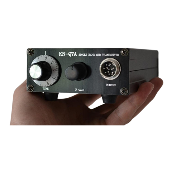
- Page 18 ] Preset the IF GAIN control to mid-way and you are ready to start alignment. After alignment, remember to install the top chassis using another 4x black chassis screws. Alignment RX Alignment In previous steps we have done most of the RX alignment. Now we are going to use an audio spectrum analyzer software (on a PC running Windows) to fine tune the BFO frequency, so the RX voice can be very clear, and more importantly, the carrier and the opposite sideband are well suppressed.
- Page 19 Remove the audio cable and connect an external speaker. Use band noise or a signal to peak again the RX BPF. Then, tune the IFT in the LO to your favorite frequency coverage. Turning it deeper means that you can get a wider frequency coverage range with a lower range end. Normally, the upper end of the range changes a little, but the lower end of the range changes much more.
-
Page 20: Theory Of Operation
The KN-Q7A is a simple design with two NE602A chips which are used both for RX and TX. When in RX, one NE602A works as first mixer plus LO to convert the received RF signal to IF, and the other works as detector plus BFO to convert the IF signal to AF. - Page 21 NE602A* MC1350 NE602A** TDA2822 C3357 D882 IRF530 8050 Voltages in TX with PTT on but no modulation @ 13.8 V, “var” means variable, * is for detector IC near BFO, and ** is for mixer IC near LO NE602A* MC1350 NE602A** TDA2822 C3357 D882 IRF530...
Need help?
Do you have a question about the KN-Q7A and is the answer not in the manual?
Questions and answers