Table of Contents
Advertisement
Specifications*
General
Power Supply
Tone Controls
Current Consumption
Maximum Power Output
Suitable Speaker Impedance
Pre-Amp Output Voltage
Output Impedance
FM Stereo Radio
Frequency Range
Usable Sensitivity
AM Radio
Frequency Range
LW Radio
Frequency Range
DC 12V (11V - 16V),
Test Voltage 14.4V
Negative Ground
Bass ; ±12dB at 100Hz
Treble ; ±12dB at 10kHz
Less than 2.2A (CD play mode,
0.5W×4ch)
50W×4ch (at 1kHz, Vol. Max.)
4-8Ω
2.5V (CD play mode; 1kHz, 0dB)
200Ω
87.5 - 108MHz
11.0dBf (1.25µV, 75Ω)
531 - 1,602kHz
153 - 279kHz
AUTOMOTIVE AFTERMARKET
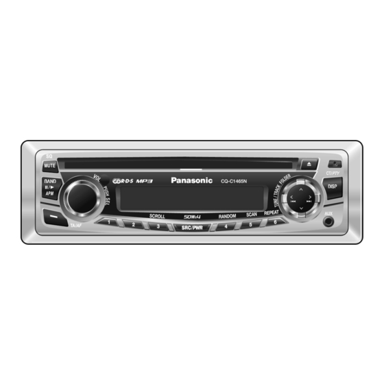
CQ-C1465N
Removable Front Panel CD Player /
Receiver
Usable Sensitivity
RDS
RDS Senstivity
CD Player
Sampling Frequency
Pick-Up Type
Light Source
Wavelength
Frequency Response
Signal to Noise Ratio
Dimensions**
Weight**
* Specifications and the design are subject to possible modification
without notice due to improvements.
** Dimensions and Weight shown are approximate.
© 2006 Matsushita Electric Industrial Co., Ltd. All
rights
reserved.
distribution is a violation of law.
Order No. ACED061209C8
28dB/µV (25µV, S/N 20dB)
22dB/µV
8 times oversampling
Astigma 3-beam
Semiconductor Laser
780nm
20Hz to 20,000Hz (±1dB)
96dB
178×50×155mm
1.4kg
Unauthorized
copying
and
Advertisement
Table of Contents

Related Manuals for Panasonic CQ-C1465N


Summary of Contents for Panasonic CQ-C1465N
-
Page 1: Specifications
Order No. ACED061209C8 AUTOMOTIVE AFTERMARKET CQ-C1465N Removable Front Panel CD Player / Receiver Specifications* General Usable Sensitivity 28dB/µV (25µV, S/N 20dB) Power Supply DC 12V (11V - 16V), Test Voltage 14.4V Negative Ground RDS Senstivity 22dB/µV Tone Controls Bass ; ±12dB at 100Hz Treble ;... -
Page 2: Table Of Contents
CQ-C1465N CONTENTS Page Page 1 ABOUT LEAD FREE SOLDER (PbF) 11 PACKAGE AND IC BLOCK DIAGRAM 2 FEATUERS 12 REPLACEMENT PARTS LIST 3 LASER PRODUCTS 13 EXPLODED VIEW (Unit) 4 REPLACEING THE FUSE 14 CD PLAYER MECHANICAL PARTS LIST 5 MAINTENANCE... -
Page 3: Maintenance
CQ-C1465N 5 MAINTENANCE Your products is designed and manufactured to ensure a minimum of maintenance. Use a dry, a soft cloth for routine exterior cleaning. Never use benzine, thinner or other solvents. 6 NOTES [RADIO BLOCK] Do not align the AM/FM package block. When the package block is necessary, it will be supplied already aligned at the factory. -
Page 4: Wiring Connection
CQ-C1465N 8 WIRING CONNECTION... -
Page 5: Block Diagram
CQ-C1465N 9 BLOCK DIAGRAM... -
Page 6: Terminals Description
CQ-C1465N 10 TERMINALS DESCRIPTION 10.1. Main Block IC601 : LC7237849D41 Ref. Part No. Part Name & FM(V AM(V CD(V Description Ref. Part No. Part Name & FM(V AM(V CD(V Description N.C. None N.C. None X’tal I 2.52 2.54 2.53 TEL_MUTE... - Page 7 CQ-C1465N Ref. Part No. Part Name & Description Ref. Part No. Part Name & Description E signal input port. 1.65 VPREF2 Built-in VCO oscillation cooking 3.25 stove setting input terminal. F signal input port. 1.66 VCOC2 Built-in VCO control voltage 1.08...
- Page 8 CQ-C1465N 10.2. Display Block IC901 : C0HBA0000223 Pin No. Port Descriptions No connection 5-39 S1-35 LCD segment 40-43 C1-4 LCD common 44-49 KS1-6 Key data output 50-54 KI1-5 Key data input TEST (Connecting to ground) +5V power supply VDD1 Ground through capacitor...
-
Page 9: Package And Ic Block Diagram
CQ-C1465N 11 PACKAGE AND IC BLOCK DIAGRAM 11.1. Main Block PA51:J3CCBC000010 IC271 : C1EA00000041... - Page 10 CQ-C1465N IC401 : C1BB00001088 IC701 : C0DAZHF00004...
- Page 11 CQ-C1465N IC251 : C1BB00000804...
- Page 12 CQ-C1465N IC551 : C1BB00000960...
-
Page 13: Replacement Parts List
CQ-C1465N 12 REPLACEMENT PARTS LIST Ref. Part No. Part Name & Description Remarks D715 B0EAJP000001 Silcon Diode D716 B0EAJP000001 Silcon Diode D717 B0EAJP000001 Silcon Diode D719 B0EAJP000001 Silcon Diode D720 B0EAJP000001 Silcon Diode D751 B0BC6R700006 Diode D871 B0ACCK000005 Diode DISPLAY BLOCK [E-4C313]... - Page 14 CQ-C1465N Ref. Part No. Part Name & Description Remarks Ref. Part No. Part Name & Description Remarks C313 F1J1H222A733 Chip 2200pF 50WV C632 F1J1H103A733 Ceramic 0.01MFD 50WV C321 F2A1H2R2A407 Electrolytic 2.2pF 50WV C651 F1J1H104A733 Ceramic 0.1MFD 50WV C322 ECQV1H224JL2 Plastic Film 0.22MFD 50WV...
- Page 15 CQ-C1465N Ref. Part No. Part Name & Description Remarks Ref. Part No. Part Name & Description Remarks D0YFR00J0001 Chip 0 ohms 1/8W R502 D0YFR00J0001 Chip 0 ohms 1/8W D0YFR00J0001 Chip 0 ohms 1/8W R503 D0YFR00J0001 Chip 0 ohms 1/8W D0YFR00J0001...
- Page 16 CQ-C1465N Ref. Part No. Part Name & Description Remarks Ref. Part No. Part Name & Description Remarks R691 D0GF473JA017 Chip 47k ohms 1/8W SW906 K0H1BA000445 Tack Swich R701 D0AZ823JA008 Chip 82k ohms 1/6W SW907 K0H1BA000445 Tack Swich R703 D0AE102JA131 Chip 1k ohms 1/4W...
- Page 17 CQ-C1465N Ref. Part No. Part Name & Description Remarks 8. Mechanical Parts MISCELLANEOUS ANT51 YEAA094C008 ANT JACK T(3-C) YFA034C053CA Upper Cover T(4-B) YGFD044C002 CD Deck T(4-C) XTB26+5FFN Screw T(4-C) XTW2+5FFN Screw T(4-C) YFF014C055CA Heat Sink T(3-C) YEJT034C019N Screw(CUP TIGHT 3X12)
-
Page 18: Exploded View (Unit)
CQ-C1465N 13 EXPLODED VIEW (Unit) -
Page 19: Cd Player Mechanical Parts List
CQ-C1465N 14 CD PLAYER MECHANICAL PARTS LIST Ref. Part No. Part Name & Description Remarks 3032 10 40 SW WIRE MN N(A-1) 3032 10 39 SP WIRE MN N(D-2) 3032 10 13 WIRE CLAMPER M N(C-2); N(C-3); N(D-4); N(E-3) 3032 10 28... -
Page 20: Exploded View (Cd Deck)
CQ-C1465N 15 EXPLODED VIEW (CD Deck) -
Page 21: Wiring Diagram
CQ-C1465N 16 WIRING DIAGRAM 16.1. Main Block-1 [E-4C312][TOP VIEW] CQ-C1475N/C1465N/C1425N/C1415N /C1405N/C1405W MAIN PCB... - Page 22 CQ-C1465N 16.2. Main Block-2 [E-4C312][BOTTOM VIEW] CQ-C1475N/C1465N/C1425N/C1415N/C1405N/C1405W MAIN PCB...
- Page 23 CQ-C1465N 16.3. Display Block [E-4C313][TOP VIEW] [E-4C313][BOTTOM VIEW] CQ-C1475N/C1465N/C1425N/C1415N /CQ-C1405N/C1405W DISPLAY PCB...
- Page 24 CQ-C1465N 16.4. CD Interface Block [E-4C288][BOTTOM VIEW] CQ-C1325N/C1315N/C1305W/C1115N/C1105W/C1105H CQ-C1304U/C1475N/C1465N/C1425N/C1415N/C1405N CD SERVO PCB...
-
Page 25: Schematic Diagram-1
CQ-C1465N 17 SCHEMATIC DIAGRAM-1 17.1. Main Block E-4C312 0.12 0.26 0.36 4.57 4.52 5.23 4.57 4.53 5.21 4.57 4.57 4.52 4.53 0.68 4.52 4.53 4.56 4.53 5.17 4.55 5.21 5.23 0.89 8.22 8.21 8.11 8.22 8.18 0.12 3.41 3.56 3.55 3.19... - Page 26 THIS PAGE IS JUST FOR THE PAGE LAYOUT USE ONLY.
-
Page 27: Schematic Diagram-2
CQ-C1465N 18 SCHEMATIC DIAGRAM-2 18.1. Display Block... - Page 28 CQ-C1465N 18.2. CD Servo Block-1...
-
Page 29: Schematic Diagram For Printing With A4 Size
CQ-C1465N 19 SCHEMATIC DIAGRAM for printing with A4 size 19.1. Main Block (Left Side) E-4C312 0.12 0.26 0.36 4.57 4.52 5.23 4.57 4.53 4.57 5.21 4.57 4.52 4.53 0.68 4.52 4.53 4.56 4.53 5.17 4.55 8.22 8.21 8.11 8.22 8.18 0.12... - Page 30 CQ-C1465N 19.2. Main Block (Right Side) E-4C312 4.57 4.52 4.57 4.53 4.57 4.57 4.52 4.53 0.68 4.52 4.53 4.56 4.53 5.17 4.55 5.21 5.23 0.89 3.25 3.25 1.83 1.08 0.08 3.29 1.23 1.84 1.04 1.65 0.88 8.06 3.25 1.34 1.34 1.37...
Need help?
Do you have a question about the CQ-C1465N and is the answer not in the manual?
Questions and answers