Advertisement
T echnical
Manual
Table of Contents
Specification..................................... 1
Appearance ......................................2
Wiring Diagram ................................ 3
Parts List ...........................................4~6
Case Outlines................................. 7~8
Disassembly Diagram....................... 9
PCB Assembly ................................. 10~11
Schematic Diagram.......................... 12
Specification
Total Harmonic Distortion + Noise
Intermodulation Distortion
Frequency Response ( ± 0.5 dB)
Channel Balance
Phase Linearity
Channel Separation
Signal to Noise Ratio
Dynamic Range
Digital to Analog Converters
Speed Accuracy, Wow & Flutter
Output Impedance
Digital Output
Load Impedance
Power Requirements
USA Version
European Version:
Power Consumption
Dimensions (W, H, D)
Panel Height
Weigt (net)
SHINSEN-BLD. 4F 10-10 SHINSEN-CHO, SHIBUYA-KU,
TOKYO 150-0045, JAPAN
Quality Uncompromised
0.0045% @ 1kHz
0.0045% @ 1kHz
20-20,000 Hz
± 0.5 dB
± 0.5 degree
> 98 dB @ 1kHz
> 100dB
> 96 dB
18 bit equivalent, multi-level Delta-Sigma DAC with
8x oversampling digital filter and HDCD
Quartz Crystal Precision
100 Ohms
0.5 Volt, Peak to Peak
75 Ohms
AC 115V, 60 Hz
AC 230V, 50 Hz
20 W atts
1
7
7
17 /
x 2
/
x 12
/
8
8
16
435 x 73 x 316 mm
3
60 mm / 2
/
"
8
5 kg, 11 lb.
®
COMPACT DISC PLAYER
RCD-02
inches
Serial. NO.
Beginning
Y-365A-0207/pdf
Advertisement
Table of Contents

Related Manuals for Rotel RCD-02


Summary of Contents for Rotel RCD-02
-
Page 1: Table Of Contents
Quality Uncompromised ® T echnical COMPACT DISC PLAYER RCD-02 Manual Table of Contents Specification........1 Appearance ........2 Wiring Diagram ........ 3 Parts List ...........4~6 Case Outlines......... 7~8 Disassembly Diagram....... 9 PCB Assembly ......... 10~11 Schematic Diagram......12 Specification Total Harmonic Distortion + Noise 0.0045% @ 1kHz... -
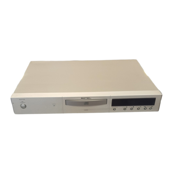
Page 2: Appearance
Appearance RCD-02 12V TRIG EXT REM DOUBLE INSULATION When servicing use only ident cal replacement par s... -
Page 4: Parts List 1/3
Parts List 1/3 SYMBOL PARTS NO. DESCRIPTION 016 X-1340A01-08 PCB ASSY 501 X-1340 PCB ASSY K201 066 4TR-2487#4 1P PIN JACK (BLK) K702 066 4TR-2487#7 1P PIN JACK (RED) K701 066 4TR-2487#8 1P PIN JACK (WHT) K451 065 YKB21-5111A 3.5Φ MINI JACK K461 065 YKB21-5103A 3.5Φ... - Page 5 Parts List 2/3 U701,702 031 OPA2604AP I C (OPE DUAL) U981 031 NJM7815FA I C (REGULATOR +15VDC) U901,931,961 031 SI3050J I C (REGULATOR +5VDC) U982 031 NJM7915FA I C (REGULATOR -15VDC) U351 031 SBX3010-52B I C (REMOTE EYE) U101 031 CXA1821M I C (RF AMP) U401 031 CXP82440A-1...
-
Page 6: Parts List
Parts List 3/3 S001 061 C-4176A08 POWER SWITCH PS3-22SPA-P7AZ TV8 T001 022 T-1060N01 POWER TRANSFOMER S731 063 A24W-K RELAY A24W-K C001 044 DE1307E472M SPARK KILLER 4700pF C701,702 044 FSC160V101H STYROL CAPACITOR 160V100pF R424 054 SE8104J THICK FILM RS 100Kx8 R423 054 SE8102J THICK FILM RS 1Kx8 T731... -
Page 7: Case Outlines
Case Outlines RCD-02 OPA2604P Vos V 2SC536K 2SA1016K NJM7805FA 2SA608K 2SC2362K SI-3050J NJM7815FA 2SB764 LB1641 TC74HCU04AP NJM7915FA CXA1821M PC817B PCM1732U CXD2545Q BA6392FP CXP82440A-179Q... - Page 8 Memo...
-
Page 9: Disassembly Diagram
Disassembly Diagram-1 Disassembly Diagram-2 ITEM DESCRIPTION SPEC. NO. ITEM DESCRIPTION SPEC. NO. ITEM DESCRIPTION SPEC. NO. 1 CHAFT(S). SLED 2-625-464-(01) 1 TRAY(S) 2-625-550-(03) 17 CHASSIS(S). OUTSERT MAIN2-625-552-(06) 2 INSULATOR(S) 2-625-538-(01) 18 SCREW+P TP WH 2.D6X16 3-319-501-(51) 3 SCREW(2X5). TAPPING(S) 2-641-386-(01) 3 COVER(S). -
Page 10: Pcb Assembly
016 X-1340 Top pattern and Silk side PCB Assembly C202 U201 C204 C207 R202 J347 S731 R923 C201 R204 D923 L201 R927 C203 J313 L202 J303 R925 J287 T924 K201 K702 K701 J304 J151 J314 C941 R928 R922 C909 J152 D731 J348 U901... - Page 11 PCB Assembly 016 X-1340 Top Silk and Bottom Pattern C202 U201 C204 C207 R202 J347 S731 R923 C201 R204 D923 L201 R927 C203 J313 L202 J303 R925 J287 T924 K201 K702 K701 J304 J151 J314 C941 R928 R922 C909 J152 D731 J348 U901...
-
Page 12: Schematic Diagram
Schematic Diagram 016 X-1340A02 K001 U351 SBX3010-52B STOP PLAY P.TRACK N.TRACK OPEN/CLOSE PAUSE S352 S353 S354 S351 S355 S356 POWER IN D351 -18.3V -29.3V C901 R354 R353 R352 R351 RD6.2JST 1.8K M 5.6K M 500V0.01 1.8K 1.8K D901 T902 2SA608K -19.0V 1N4003 D001...
Need help?
Do you have a question about the RCD-02 and is the answer not in the manual?
Questions and answers