Table of Contents
Advertisement
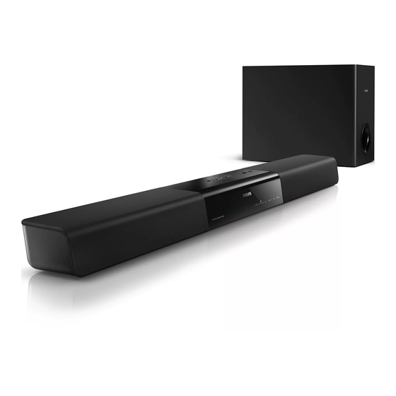
Home Theater Soundbar
Service
Service Manual
. Location of PCB Boards,Version Variation and Repair Scenario Matrix.....1-2
. Technical Specifications.........................................................1- 3
. Safety Instruction, Warning & Notes........................................1- 4
. DFU Instruction..............................................................................2-1
. Mechanical and Dismantling Instructions....................................3-1
. Software Upgrades .......................................................................
. Trouble Shooting Chart......................................................
. Wiring Diagram..................................................................6-1
. Electrical Diagrams and Print-layouts......................................7-1
. Votages and Waveforms for Connection Pins...........................8-1
. Pin Description & Block Diagrams of ICs..................................9-1
. Set Mechanical Exploded view & Part list...............................10-1
. Revision List.................................................................................11-1
©Copyright 2011 Philips Consumer Electronics B.V. Eindhoven, The Netherlands
All rights reserved. No part of this publication may be reproduced, stored in aretrieval system or
transmitted, in any form or by any means, electronic, mechanical, photocopying, or otherwise
without the prior permission of Philips.
Published by Arya & Stephen - 1252 BU AVM Printed in The Netherlands Subject to modification
Version 1.2
TABLE OF CONTENTS
HTL2160C/G/M/S/T/W/12/F7/93
Page
4-1
.
5-1
.
PHILIPS
CLASS 1
LASER PRODUCT
3141 785 38622
GB
Advertisement
Table of Contents

Related Manuals for Philips HTL2160C/G/M/S/T/W/12/F7/93


Summary of Contents for Philips HTL2160C/G/M/S/T/W/12/F7/93
- Page 1 . Set Mechanical Exploded view & Part list.…………………..….…10-1 . Revision List.................11-1 CLASS 1 ©Copyright 2011 Philips Consumer Electronics B.V. Eindhoven, The Netherlands All rights reserved. No part of this publication may be reproduced, stored in aretrieval system or LASER PRODUCT transmitted, in any form or by any means, electronic, mechanical, photocopying, or otherwise without the prior permission of Philips.
- Page 2 PCB BOARD LOCATION: FK BOARD OP BOARD OP BOARD CN BOARD MAIN BOARD POWER BOARD VERSION VARIATIONS Type / Versions HTL2160 Service Policy Board in used MAIN BOARD MAIN BOARD FRONT BOARD POWER BOARD C -- Component Lever Repair Tips: *...
- Page 3 HTL2160/12/F7: Frequency response: 20 Hz-150 Hz Product Dimensions (WxHxD): 165 x 240 x 295 specifications Weight: 2.6 kg Cable length: 3 m Remote control batteries Note 1 x CR2025 notice. Total output power: 40W RMS (+/- 0.5 dB, 10% THD) Frequency response: 20 Hz-20 kHz / ±3 Signal-to-noise ratio: >...
- Page 4 HTL2160/93: Product Bluetooth specifications Bluetooth version: 2.1 + EDR Main unit Power supply: 220-240 V~, 50 Hz - 60 Hz Note Power consumption: 30 W notice. Speaker impedance: 8 ohm (Tweeter), 4 ohm (Woofer) Frequency response: 160 Hz-20 kHz Dimensions (WxHxD): 800 x 75.6 x 52.4 Total output power: 60W RMS (+/- 0.5 dB, Weight: 1.2 kg 10% THD)
-
Page 5: Safety Instruction, Warning & Notes
Safety instruction, Warning & Notes Safety instruction 1. General safety 2.Laser safety Safety regulations require that during a repair: This unit employs a laser. Only qualified service personnel . Connect the unit to the mains via an isolation transformer. may remove the cover, or attempt to service this device . - Page 6 Warning 1.General 2. Laser . All ICs and many other semiconductors are susceptible to . The use of optical instruments with this product, will electrostatic discharges (ESD). Careless handing during increase eye hazard. repair can reduce life drastically. Make sure that, during .
- Page 7 Solder Joint...
- Page 8 - lead free BGA-ICs will be delivered in so-called respected by the workshop during a repair: ‘dry-packaging’ (sealed pack including a silica gel Use only lead-free solder alloy Philips SAC305 with pack) to protect the IC against moisture. After order code 0622 149 00106. If lead-free solder-paste is...
-
Page 9: Remote Control
AUDIO-IN: Lights up when you switch to the audio input source. Congratulations on your purchase, and h SURR Lights up when you select Virtual Surround the support that Philips offers, register your sound. SoundBar at www.philips.com/welcome. i Bluetooth Lights up when you switch to the Main unit Bluetooth mode. - Page 10 f TREBLE +/- Increase or decrease treble. g SURR Toggle between stereo and virtual surround sound. Mute or restore volume. i BASS +/- Increase or decrease bass. j +/- Increase or decrease volume. k AUDIO-IN Switch your audio source to audio in connection.
- Page 11 Connect Rear connectors This section helps you connect your SoundBar to a TV and other devices. For information about the basic connections of your SoundBar and accessories, see the quick start guide. Note plate at the back or bottom of the product. Before you make or change any connections, make sure that all devices are disconnected from the power outlet.
-
Page 12: Other Devices
Option 1: Connect audio through a digital optical cable Connect Best quality audio Connect your subwoofer to your SoundBar as described in the quick start guide. Connect audio from TV and other devices Play audio from TV or other devices through Using an optical cable, connect the your Soundbar speakers. - Page 13 the OPTICAL OUT connector on the TV or other device. The digital optical connector might be labeled SPDIF or SPDIF OUT. Option 2: Connect audio through a digital coaxial cable Best quality audio Using a coaxial cable, connect the COAXIAL connector on your SoundBar to the COAXIAL/DIGITAL OUT connector on the TV or other device.
- Page 14 Mechanical and Dismantling Instructions Dismantling Instruction Detailed information please refer to the model set. The following guidelines show how to dismantle the player. Step1: Dismantle the Right Speaker and Left Speaker. Remove 4 screws on the Bottom Cover. Then pull out the speakers.(Figure 1) (Figure 1) Step2: Open the Top Cover.Remove 6 screws on the Bottom Cover.
- Page 15 Mechanical and Dismantling Instructions Dismantling Instruction Detailed information please refer to the model set. Step3: Dismantle the Power Board and Main Board.remove 5 screws on the boards and 3 screws on the Bottom Cover. Disconnect connector CN503. Pull out the Main Board,then pull out the Power Board.(Figure 3) CN503 (Figure 3) Step4: Dismantle the Front and key board.
-
Page 16: Software Upgrades
Software Upgrade Step1: Main board software Update procedure: 1. Rename upgrade file to mpeg2160_XX.bin (XX means different area code). Copy mpeg2160_XX.bin to root directly of USB disk. 2. Plug USB in ,then Switch source to USB It will be auto upgrade software and all LEDs will turn on while upgrading, Strongly suggest do not operate it when upgrading. -
Page 17: Trouble Shooting Chart
Trouble shooting Chart No +19V output No +19V output F501 Replace the F501(Use the (Fuse3.15A) normal? same ICW) Is the D533/D534 Replace the normal D538/D539/D540/D541 Is the U531 Replace the U531 (TOP258EN) normal Is the D531 D532 Replace the D531 D532 U533 U533 normal Is there about 15V at Replace the U532... - Page 18 Trouble shooting Chart no display on LED board no display on LED board Check every supply check the power supply board voltage on main board whether normal or not +18V +3.3V Check every supply check the FFC connector from voltage on front board main board to front board whether normal or not +5V +3.3V .
- Page 19 Trouble shooting Chart Remote control does not work Remote control does not work Check the battery of Replace the battery for remote remote control control exhausted or not Check power Check the 3.3V_STB weather supply of IR1 on normal or not main board whether Replace the IR1...
- Page 20 Trouble shooting Chart No audio output No audio output Make sure have Choose the right channel choose the right channel Check the signal input is Change the signal source good Check the +18V on main Change the signal source board whether normal or Check +3.3V Change the main board...
- Page 21 Block Diagram for HTL2160: Bluetooth Coaxial Coaxial 74HC04 TAS3159 SPDIF TAS3159 SDRAM Optical SPHE8202R SPHE8202R 74HC4052 AKM5358 Flash Aux in EN*1 UART/reset I/O*5 I/O*1 Subwoofer TAS5711 RST/PDN M054 15W 2+30W(THD+N) I/O*1 Bluetooth Power AMP 20V SWITCH ADC_5V/USB_5V EUP3482A SWITCH LD1117 3.3V LDO_G9091 330T11U...
- Page 22 OP Board Circuit Diagram for HTL2160/12/F7/93: CON_6PIN _2*3 CON_6PIN _2*3...
- Page 23 CN Board Circuit Diagram for HTL2160/12/F7/93: LED4 LED4 LED5 LED5 LED6 LED6 LED_AMBER LED_AMBER LED_AMBER LED_AMBER LED_AMBER LED_AMBER COAX_LED OPT_LED iLINK_LED NPN_3DG3904M NPN_3DG3904M NPN_3DG3904M NPN_3DG3904M NPN_3DG3904M NPN_3DG3904M 4.7K 4.7K 4.7K 4.7K 4.7K 4.7K 4.7K 4.7K 4.7K 4.7K 4.7K 4.7K BT_LED POWER_LED AUX_LED iLINK_LED...
- Page 24 FK Board Circuit Diagram for HTL2160/12/F7/93: 6.8pF/50V/NP0 6.8pF/50V/NP0 NC/0 NC/0 NC/0 NC/0 BT_33 220K 220K AIO1 AIO0 MIC_A_N BT_RST BT_RST RESET MIC_A_P MIC_B_N PIO9 MIC_B_P PIO1 0 MIC_BIAS PIO11 GND_S BT_33 NC 0.1uF/25V/Y5V NC 0.1uF/25V/Y5V BT_POWER PIO12 SPK_R_P PIO13 SPK_R_N PIO14 SPK_L_P PIO15...
- Page 25 FK Board Circuit Diagram for HTL2160/12/F7/93: 24PIN/0.5mm 24PIN/0.5mm 100pF/50V/NP0 100pF/50V/NP0 MCU_3V3 MCU_3V3 MCU_3V3 +3.3V_STB 500/500mA 500/500mA MCU_RST 500/500mA 500/500mA MCU_RST 10uF/16V 10uF/16V SPDIF_SW2 12MHz/30PPM 12MHz/30PPM C165 C165 SPDIF_SW1 AMP_RST 10pF/50V/NP0 10pF/50V/NP0 20pF/50V/NP0 20pF/50V/NP0 20pF/50V/NP0 20pF/50V/NP0 AMP_SCL 10uF/16V 10uF/16V AMP_SDA 4052_SW POWER_ON/OFF IR_IN MPEG_RST...
- Page 26 Power Board Circuit Diagram for HTL2160/12/93: TR501 TR501 T501 T501 FB504 FB504 KBP306 KBP306 LIF4-22-15 LIF4-22-15 NTC/3ohm/5A NTC/3ohm/5A FB90@100MHz FB90@100MHz R502C R502C 220pF/250VAC 220pF/250VAC CN5011 CN5011 R502A R502A +18V CY502 CY502 LIF501 LIF501 PWS004 PWS004 CE502 CE502 CN501 CN501 RV501 RV501 LIF503 LIF503...
- Page 27 Power Board Circuit Diagram for HTL2160/F7: TR501 TR501 T501 T501 FB504 FB504 KBP306 KBP306 LIF4-22-15 LIF4-22-15 NTC/3ohm/5A NTC/3ohm/5A FB90@100MHz FB90@100MHz R502C R502C 470pF/250VAC 470pF/250VAC CN5011 CN5011 R502A R502A +18V CY502 CY502 LIF501 LIF501 PWS004 PWS004 CE502 CE502 CN501 CN501 RV501 RV501 LIF503 LIF503...
- Page 28 Main Board Circuit Diagram for HTL2160/12/F7/93:Power POWER_20V 300/2A 300/2A 6PIN/2.5mm/120mm 6PIN/2.5mm/120mm POWER_20V POWER_20V 220uF/35V 220uF/35V STBY+5V AP4435GM AP4435GM 330pF/50V/NP0 330pF/50V/NP0 VCC_AMP 300/2A 300/2A 10uH/2A 10uH/2A 300/2A 300/2A CE16 CE16 0.01uF/50V/X7R 0.01uF/50V/X7R 220uF/35V 220uF/35V 4.3K/1% 4.3K/1% NC/56 NC/56 220uF/16V 220uF/16V 220/1% 220/1% EUP3482A EUP3482A...
- Page 29 Main Board Circuit Diagram for HTL2160/12/F7/93:MP3 & AUX 2.2uF/10V/Y5V 2.2uF/10V/Y5V MP3_AR MP3_AL AL_CH1 MP3_AL 3PIN/2.0mm 3PIN/2.0mm 2.2uF/10V/Y5V 2.2uF/10V/Y5V MP3_AR AR_CH1 VCC_AMP AUX_L AUX_L 8.2K 8.2K 2.2uF/10V/Y5V 2.2uF/10V/Y5V AL_CH3 2.4K 2.4K AUX_L 47uF/16V 47uF/16V 8.2K 8.2K AUX_R 8.2K 8.2K 2.2uF/10V/Y5V 2.2uF/10V/Y5V AR_CH3 AUX_R 8.2K...
- Page 30 Main Board Circuit Diagram for HTL2160/12/F7/93:COAX & OPT & BT 5V-OPT A5_5V AUXIN_LL AUX_L AUX_L AGND 5V-OPT COAX COAX_IN AUXIN_RR AUX_R AUX_R OPT_IN NC/200 NC/200 AUXIN_RR AUXIN_LL COAX 0.1uF/25V/X7R 0.1uF/25V/X7R COAX OPT_IN OPT_IN2 A5_5V SPD_VCC 0.1uF/25V/X7R 0.1uF/25V/X7R COAX_IN 1.8uH/25mA 1.8uH/25mA A5_5V SPDIF_SW1 SPDIF_SW1...
- Page 31 7-10 7-10 Main Board Circuit Diagram for HTL2160/12/F7/93:SP8202 4.7K 4.7K RF3.3V VVCC3 500/200mA 500/200mA 27MHz/30PPM 27MHz/30PPM FV33 DV33 33pF/50V/NP0 33pF/50V/NP0 33pF/50V/NP0 33pF/50V/NP0 VCC1.2 DVCC3 DVCC3 FB11 FB11 500/200mA 500/200mA VCC1.2 Put these Compnonents as 4.7uF/16V/Y5V 4.7uF/16V/Y5V closer as possible to MT1389 SF_CS SPI_D0...
- Page 32 7-11 7-11 Main Board Circuit Diagram for HTL2160/12/F7/93:TAS5711 15W*2 THD+N=10% R=8ohm 4700pF/50V/X7R 4700pF/50V/X7R 4700pF/50V/X7R 4700pF/50V/X7R 0.047uF/50V/X7R 0.047uF/50V/X7R 0.047uF/50V/X7R 0.047uF/50V/X7R C87 0.033uF/50V/X7R C87 0.033uF/50V/X7R 22uH/3.3A 22uH/3.3A VCC_AMP1 VCC_AMP FB16 FB16 CE10 CE10 220uF/35V 220uF/35V VCC_AMP SYS_3V3 CE11 CE11 C133 C133 3.3UF 3.3UF 0.47uF/25V/Y5V 0.47uF/25V/Y5V...
- Page 33 7-12 7-12 Main Board Circuit Diagram for HTL2160/12/F7/93:IR 24PIN/0.5mm 24PIN/0.5mm +3.3V_STB +3.3V_STB A5_5V MCU_3.3V FB21 FB21 500/500mA 500/500mA R110 R110 FB22 FB22 500/500mA 500/500mA 4.7K 4.7K IRM_8.3mm IRM_8.3mm IR_IN R111 R111 R112 R112 +3.3V_STB R118 1K R118 1K SPDIF_SW2 R117 1K R117 1K R119 1K R119 1K...
- Page 34 7-13 7-13 OP Board Print-layout(Bottom side):...
- Page 35 7-14 7-14 CN Board Print-layout(Bottom side):...
- Page 36 7-15 7-15 CN Board Print-layout(Top side):...
- Page 37 7-16 7-16 FK Board Print-layout(Bottom side):...
- Page 38 7-17 7-17 FK Board Print-layout(Top side):...
- Page 39 7-18 7-18 Power Board Print-layout(Bottom side):...
- Page 40 7-19 7-19 Main Board Print-layout(Bottom side):...
- Page 41 7-20 7-20 Main Board Print-layout(Top side):...
- Page 42 Voltages for per connection pin XS1 from power supply board connect to main board XS1 from power supply board connect to main board Pin NO. Pin Assin Remarks 18‐20V XP5 from main board connect to front board Pin NO. Pin Assin Remarks MCU 3 3v MCU_3.3v 3 2V 3 4V 3.2V‐3.4V A5_5V 4.75‐5.25V SPDIF_SW2 SPDIF_SW1 AMP_RST AMP_SCL AMP_SDA 4052_SW POWER_OM/OFF IR IN IR_IN MPEG_RST ADC_RST XP2 from main board connect to front board for USB...
- Page 43 Main IC-SP8202_RDB Functional Block Diagram...
- Page 44 Main IC-SP8202_RDB PIN Description Symbol Pin # Description VFD_CLK/GPIO 1. CLK of VFD 2. General-purpose I/O VFD_STB/GPIO 1. Strobe of VFD 2. General-purpose I/O VFD_DATA/GPIO 1. DATA of VFD 2. General-purpose I/O VDD33 I/O power supply RST_B System Reset VSS_0 Ground IR_I/GPIO IR input or general-purpose I/O...
- Page 45 Main IC-SP8202_RDB PIN Description Symbol Pin # Description M_CLKO SDRAM CLK VDD33 I/O power supply M_A11/GPIO 1. SDRAM address bus 11 2. General-purpose I/O 3. UA0_RXD : UART RX Port 1 4. HSYNC_PC : HSYNC signal of TV Interface M_A9 SDRAM address bus 9 M_A8 SDRAM address bus 8...
- Page 46 Main IC-SP8202_RDB PIN Description Symbol Pin # Description VSS_ADAC_1 Ground pin for Audio DAC #1 AOUT_FL DAC Front Left channel analog output AOUT_FR DAC Front Right channel analog output Video DAC Interface V_COMP Video DAC Bias Voltage V_FSADJ Full-Scale adjust control pin (EXT resistor) (1.2 K ohm to ground) TV_DAC0 Video DAC channel 0 output VDD_TVA0...
-
Page 47: Figure
Main IC-SP8202_RDB PIN Description Symbol Pin # Description OPVIN Op-amp 1 negative input RF_APC_AVSS Ground pin for RF and APC DVDLDO DVD APC output CDLDO CD APC output DVDMDI DVD APC input from monitor photo diode CDMDI CD APC input from monitor photo diode SRV_AVDD 3.3V power for SERVO Reference DC bias voltage... - Page 48 Main IC-SP8202_RDB PIN Description Symbol Pin # Description CDVR/GPIO 1. HW_CFG_SRC[3] : Hardware Configure bit 3 2. General-purpose I/O 3. Servo CDVR SPI_CSB/GPIO 1. Chip Select of SPI Interface 2. General-purpose I/O SPI_D0/GPIO 1. Data bit 0 of SPI Interface 2.
- Page 49 10-1 10-1 Exploded View for HTL2160/12/F7/93:...
-
Page 50: Revision List
11-1 REVISION LIST Version 1.0 * Initial release for HTL2160/12/F7 Version 1.1 * Add the color v ersion for /12 on cov er. Version 1.2 * Initial release for HTL2160/93.
Need help?
Do you have a question about the HTL2160C/G/M/S/T/W/12/F7/93 and is the answer not in the manual?
Questions and answers