Table of Contents
Advertisement
Quick Links
Specifications
n AMPLIFIER SECTION
Recording system
Optical pick-up
Recordable discs
Recording time
Discs played
DVD video recording format (DVD-
RAM),
DVD video format (DVD-R)
Systemwith 1 lens, 2 integration
units (658 nm wavelength for
DVDs, 795 nm wavelength for
12 cm 4.7 GB DVD-RAM discs
12 cm 9.4 GB DVD-RAM discs
8 cm 2.8 GB DVD-RAM discs
8 cm 1.4 GB DVD-R discs (for
General Ver. 2.0)
12 cm 4.7 GB DVD-R discs (for
General Ver. 2.0)
12 cm 4.7 GB DVD-R discs (for
General Ver. 2.0/ 4X-SPEED
DVD-R Revision 1.0)
Max. 8 hours (using 4.7 GB disc)
XP: 60 minutes
SP: 120 minutes
LP: 240 minutes
EP: 360 minutes or 480 minutes
12 cm 4.7 GB DVD-RAM discs
12 cm 9.4 GB DVD-RAM discs
8 cm 2.8 GB DVD-RAM discs
12 cm 4.7 GB DVD-R discs (for
General Ver. 2.0)
8 cm 1.4 GB DVD-R discs (for
General Ver. 2.0)
12 cm 4.7 GB DVD-R discs (for
General Ver. 2.0/ 4X-SPEED
DVD-R Revision 1.0)
DVD-VIDEO discs
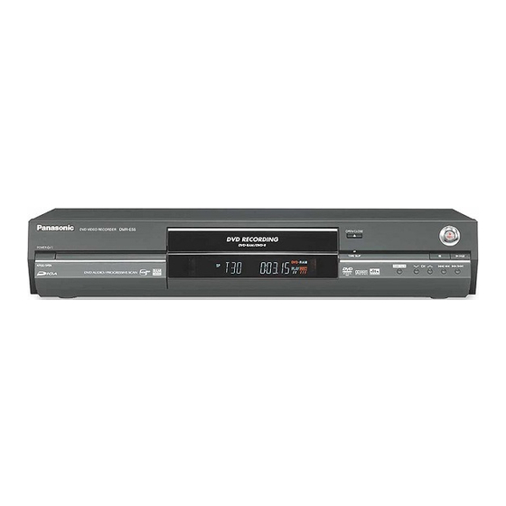
DMR-E55PL
Colour
(S).......................Silver Type
n VIDEO SYSTEM
CDs)
TV system
Recording system
Input
Output
Component video output
(480P/480i)
Antenna reception input
n AUDIO SYSTEM
Recording system
Input
© 2004 Panasonic AVC Networks Singapore Pte.
Ltd. (RCB REGISTRATION NUMBER: 197701580H)
All rights reserved. Unauthorized copying and
distribution is a violation of law.
ORDER NO.MD0405181C3
DVD Video Recorder
DVD-Audio discs
CD-Audio discs (CD-DA)
Video CD discs
CD-R/ CD-RW discs (CD-DA,
Video CD, MP3 formatted discs)
NTSC system, 525 lines, 60 fields
PAL-M system, 525 lines, 60 fields
(PAL-M: Entrance only)
MPEG2 (Hybrid VBR)
LINE (pin jack) x3, 1.0 Vp-p; 75 Ω
S connector x3
Y: 1.0 Vp-p; 75 Ω
C: 0.286 Vp-p; 75 Ω
LINE (pin jack) x1, 1.0 Vp-p; 75 Ω
S connector x1
Y: 1.0 Vp-p; 75 Ω
C: 0.286 Vp-p; 75 Ω
Y: 1.0 Vp-p; 75 Ω
PB: 0.7 Vp-p; 75 Ω
PR: 0.7 Vp-p; 75 Ω
VHF Channel: 2ch-13ch, 75 Ω
UHF Channel: 14ch-69ch, 75 Ω
CATV Channel: 5A & A-5ch-
LINE (pin jack) x3
Reference input: 309mVrms
FS: 2 Vrms (1 kHz, 0 dB)
EEEch, 75 Ω
Dolby Digital
Advertisement
Table of Contents

Related Manuals for Panasonic DMR-E55PL


Summary of Contents for Panasonic DMR-E55PL
-
Page 1: Specifications
General Ver. 2.0/ 4X-SPEED DVD-R Revision 1.0) Reference input: 309mVrms DVD-VIDEO discs FS: 2 Vrms (1 kHz, 0 dB) © 2004 Panasonic AVC Networks Singapore Pte. Ltd. (RCB REGISTRATION NUMBER: 197701580H) All rights reserved. Unauthorized copying and distribution is a violation of law. -
Page 2: Table Of Contents
DMR-E55PL Output impedance: 47 kΩ Wave length 795 nm 658 nm Output LINE (pin jack) x1 Laser power No hazardous radiation is emitted with the safety protection Reference output: 309mVrms Power supply AC 110-240, 50/60 Hz FS: 2 Vrms (1 kHz, 0 dB) - Page 3 DMR-E55PL 19.6. DIGITAL (GLUE NET) CIRCUIT (GN) 21 Wiring Connection Diagram 19.7. DIGITAL (RSTC) CIRCUIT (EN) 22 Illustration of IC 痴, Transistors and Diodes 19.8. DIGITAL (AV DECODER/MAIN CPU) CIRCUIT (MC) 23 Exploded Views 19.9. DIGITAL (AUDIO I/O) CIRCUIT (AI) 23.1.
-
Page 4: Safety Precautions
DMR-E55PL 1 Safety precautions 1.1. General guidelines 1. When servicing, observe the original lead dress. If a short circuit is found, replace all parts which have been overheated or damaged by the short circuit. 2. After servicing, see to it that all the protective devices such as insulation barriers, insulation papers shields are properly installed. -
Page 5: Prevention Of Electrostatic Discharge (Esd) To Electrostatic Sensitive (Es) Devices
DMR-E55PL 2 Prevention of Electrostatic Discharge (ESD) to Electrostatic Sensitive (ES) Devices Some semiconductor (solid state) devices can be damaged easily by static electricity. Such components commonly are called Electrostatic Sensitive (ES) Devices. Examples of typical ES devices are integrated circuits and some field-effect transistor- sandsemiconductor "chip"... -
Page 6: Precaution Of Laser Diode
DMR-E55PL 3 Precaution of Laser Diode... -
Page 7: How To Replace The Lithium Battery
( As shown in 20.1. The Main P.C.B. ) NOTE: The lithium battery is a critical component. ( Type No.: CR2354-1GUF Manufactured by Panasonic. ) It must never be subjected to excessive heat or discharge. It must therefore only be fitted in equipment designed specifically for its use. -
Page 8: Each Buttons
DMR-E55PL 6 Each Buttons... -
Page 9: New Features
DMR-E55PL 7 New Features 7.1. Function of Power Circuit (IC1150) 1. General We adopted IC module as the Switching Power Circuit for lower power consumption. IC1150 is constructed with Switching materials and Control IC, and is partial resonance module. We realized Switching Power with high efficiency, low noise and low power consumption. -
Page 10: Display
DMR-E55PL Startup Circuit Timing Chart Function of Z/C Terminal When voltage of Z/C reaches 0.25V, Gate signal is output and Drain current starts to flow. Function of F/B terminal F/B signal decides Switching ON width in low voltage controlling. The Switching ON width responds to change of F/B Voltage. -
Page 11: Display
DMR-E55PL IC1150 Block Diagram Signal name Pin No. Name Symbol Zero Current Det. Feed back Drain Drain... -
Page 12: Taking Out The Disc From Ram-Drive Unit When The Disc Cannot Be Ejected By Open/Close Button
DMR-E55PL 8 Taking out the Disc from RAM-Drive Unit when the Disc cannot be ejected by OPEN/CLOSE button 8.1. Forcible Disc Eject 8.1.1. When the power can be turned off. 1. Turn off the power and press [STOP] [CH UP] keys on the front panel simultaneously for 5 seconds. -
Page 13: Service Explorer
DMR-E55PL 9 Service Explorer Confirm “RAM-Drive Last Error” in Service Mode Execute Service Mode 1. Press [STOP], [TIME SLIP] and [OPEN/CLOSE] simultaneously for 5 seconds when P-off. FL Display: *After finishing display “(7). Factor of Drive Error occurring”, press [0] [2] ~[9] [9] keys of the Remote Controller so that 99 memories can be displayed as maximum. -
Page 14: Display
DMR-E55PL (5) Error occurring Disc type is displayed for 5 seconds. (6) Disc Maker´s ID is displayed for 5 seconds. Example of Disc Maker´s ID: DVD-R Disc FL Display (Disc Maker´s ID) Disc Maker Country Panasonic Japan Pioneer Japan Mitsubishi Chemical Corporation... -
Page 15: Display
DMR-E55PL Error Occurring Disc State... -
Page 16: Self-Diagnosis And Special Mode Setting
DMR-E55PL 10 Self-Diagnosis and Special Mode Setting 10.1. Self-Diagnosis Functions Self-Diagnosis Function provides information for errors to service personnel by “Self-Diagnosis Display” when any error has occurred. U14, H** and F** are stored in memory and held. Display on FL will be cancelled when the power is turned off or AC input is turned off during self-diagnosis display is ON. -
Page 17: Special Modes Setting
DMR-E55PL 10.2. Special Modes Setting Item FL display Key operation Mode name Description Front Key TEST Mode *All the main unit´s parameters (include tuner) Press [SKIP (REV)], [TIME SLIP] are initialized. [OPEN/CLOSE] keys simultaneously for five seconds when power is off. -
Page 18: Display
DMR-E55PL Aging Contents (Example):... -
Page 19: Service Modes
DMR-E55PL 10.3. Service Modes Service mode setting: While the power is off, press TIME SLIP, STOP and OPEN / CLOSE simultaneously for five seconds. Item FL display Key operation Mode name Description (Remote controller key) Release Items Item of Service Mode executing is cancelled. -
Page 20: Display
DMR-E55PL Item FL display Key operation Mode name Description (Remote controller key) White Picture Output White picture is output as component Output *Initial mode is “Interlace”. Press [1] [1] in service mode. from AV Decoder. *White picture (Saturation rate : 100%) -
Page 21: Display
DMR-E55PL Item FL display Key operation Mode name Description (Remote controller key) RAM Drive Last Error RAM Drive error code display. 1. Error Number is displayed for 5 Press [4] [2] in service mode. *For details about the drive error code, refer seconds. -
Page 22: Display
DMR-E55PL Item FL display Key operation Mode name Description (Remote controller key) Display the accumlated Display the accumulated unit´s working time. Press [6] [4] in service mode. working time (Indicating unit: Second) Display the Error History Display the Error History stored on the unit. -
Page 23: Assembling And Disassembling
DMR-E55PL 11 Assembling and Disassembling 11.1. Disassembly Flow Chart The following chart is the procedure for disassembling the casing and inside parts for internal inspection when carrying out the servicing. To assemble the unit, reverse the steps shown in the chart below. -
Page 24: Top Case
DMR-E55PL 11.3. Top Case 1. Remove the 2 screws (A) and 3 screws (B). 2. Open the both ends at rear side of the Top Case a little and lift the Top Case in the direction of the arrows. 11.5. Front Panel 1. -
Page 25: Panel P.c.b
DMR-E55PL 11.8. Rear Panel 1. Remove the 5 screws (A) and screw (B). 2. Unlock 2 Locking Tabs to remove Rear Panel. 11.6. Panel P.C.B. 1. Remove 6 screws and Front Angle. 11.8.1. Only Fan Motor 1. Remove the 2 screws. -
Page 26: Main P.c.b
DMR-E55PL 11.9. Main P.C.B. 11.10. Power P.C.B. 1. Remove the 5 screws (A), Connector (A) and Fan 1. Remove 3 Screws and Connector (A). Connector. 2. Lift up Power P.C.B. a little so to unlock 2 Tabs and slide Power P.C.B. so to unlock Flange to remove Power P.C.B. -
Page 27: Service Fixture And Tools
DMR-E55PL 12 Service Fixture and Tools Part Number Description Compatibility RFKZ0125 Extension FFC (Digital P.C.B. - DVD-RAM Drive / 40 Pin) Same as E50 series RFKZ0168 Extension Cable (Main P.C.B. - Fan / 3 Pin) Same as E50 series RFKZ0197 Extension Cable (Main P.C.B. -
Page 28: Service Positions
DMR-E55PL 13 Service Positions Note: For description of the disassembling procedure, see the section 11. 13.1. Checking and Repairing of Power P.C.B. -
Page 29: Checking And Repairing Of Main P.c.b
DMR-E55PL 13.2. Checking and Repairing of Main P.C.B. -
Page 30: Checking And Repairing Of Digital P.c.b
DMR-E55PL 13.3. Checking and Repairing of Digital P.C.B. -
Page 31: Checking And Repairing Of Dvd-Ram Drive
DMR-E55PL 13.4. Checking and Repairing of DVD-RAM Drive... -
Page 32: Adjustment Procedures
Turn on the power, and confirm items pointed out. Items pointed out should reappear. Insert RAM disc. The Panasonic RAM disc should be recognized. Enter the EE (TU IN / AV IN - AV OUT) mode. No abnormality should be seen in the picture, sound or operation. -
Page 33: Voltage And Waveform Chart
DMR-E55PL 16 Voltage and Waveform Chart Note) · Indicated voltage values are the standard values for the unit measured by the DC electronic circuit tester (high-impedance) with the chassis taken as standard. Therefore, there may exist some errors in the voltage values, depending on the internal impedance of the DC circuit tester. -
Page 34: Display
DMR-E55PL IC4001 Ref No. MODE PLAY STOP IC4004 IC4005 IC7404 Ref No. MODE 13.4 PLAY 13.4 STOP 13.4 IC7501 Ref No. MODE PLAY STOP IC7501 Ref No. MODE PLAY STOP IC7501 Ref No. MODE PLAY STOP IC7501 Ref No. MODE... -
Page 35: Panel P.c.b
DMR-E55PL 16.3. Panel P.C.B. Ref No. QR7801 MODE PLAY STOP 16.4. P9001 Connector Ref No. P9001 MODE PLAY STOP P9001 Ref No. MODE PLAY STOP P9001 Ref No. MODE PLAY STOP P9001 Ref No. MODE PLAY STOP P9001 Ref No. -
Page 36: P9001 Waveform
DMR-E55PL 16.5. P9001 Waveform T1150-3 STOP T1150-4 STOP T1150-6 STOP T1150-8 STOP 29Vp-p (5 sec.div) 11Vp-p (5m sec.div) 15Vp-p (5 sec.div) 330Vp-p (5 sec.div) T1150-9,10 STOP IC1150-1 STOP IC1150-2 STOP P7402-2 REC/PLAY 15Vp-p (5 sec.div) 8.0Vp-p (5 sec.div) 1.9Vp-p (5 sec.div) 0.8Vp-p (20 sec.div) -
Page 37: Abbreviations
DMR-E55PL 17 Abbreviations INITIAL/LOGO ABBREVIATIONS INITIAL/LOGO ABBREVIATIONS A0~UP ADDRESS ERROR TORQUE CONTROL ACLK AUDIO CLOCK ERROR TORQUE CONTROL AD0~UP ADDRESS BUS REFERENCE ADATA AUDIO PES PACKET DATA ENCSEL ENCODER SELECT ADDRESS LATCH ENABLE ETMCLK EXTERNAL M CLOCK (81MHz/40.5MHz) AMUTE AUDIO MUTE... -
Page 38: Display
DMR-E55PL INITIAL/LOGO ABBREVIATIONS INITIAL/LOGO ABBREVIATIONS READ ENABLE VBLANK V BLANKING RFENV RF ENVELOPE COLLECTOR POWER SUPPLY RF PHASE DIFFERENCE OUTPUT VOLTAGE (CD-ROM) REGISTER SELECT VCDCONT VIDEO CD CONTROL (TRACKING RSEL RF POLARITY SELECT BALANCE) RESET DRAIN POWER SUPPLY VOLTAGE RESERVE... -
Page 39: Block Diagram
DMR-E55PL 18 Block Diagram T001 L001,L002 D001 ~ D004 ETB28BF1U6A POWER TRANSFORMER AC SOCKET F001 P001 (250V2A) SURGE SUPPRESSOR RECTIFIER SURGE ABSORBER STRG6353 (SW IC) PC001 Q106 PHOTO COUPLER Q113 COLD... -
Page 40: Display
DMR-E55PL POWER P.C.B. MAIN P.C.B. F101 Q105 SBM40 D+1.8V PS102 P1502 21,22 IC103 SI3010KM (REG.+5V) D+3.3V PS102 P1502 19,20 Q115 F102 SBM32 X SW+5.9V PS102 P1502 DR+12V PS102 P1502 P1501 P102 (TO DVD RAM DRIVE) 12,13 IC106 SI3120J (REG.+5V) PS101... -
Page 41: Display
DMR-E55PL IC1509 C0DBEFG00003 (REG.D+1.2V) 1 VIN VOUT IC1510 2 VB C0DBEGG00003 (REG.D+1.5V) D+1.8V VOUT IC7505 IC7501- C0EBE0000194 (SYS PFAIL OUT) QR7502 (SYS PFAIL OUT) D+3.3V IC1508 C0DBEGD00002 (REG.ANA+3.3V) VOUT X SW+5.8V IC4004 POWER ON C0CBCDC00026 (REG.AU+5V) VOUT IC3001 (+5V) IC1502 C0DBAHG00013 (REG.JC+5V) -
Page 42: Display
DMR-E55PL MAIN P.C.B. REG.D+1.2V P7402 P9001 IC6001(+1.2V) 82,86,88 REG.D+1.5V P7402 P9001 IC3404(+1.5V) 78,80,84 IC3401/IC3402/IC3404/IC3408/ D+3.3V P7402 P9001 IC4403/IC6001/IC6002/IC6003/ IC6004/IC6005/IC50001/ 74,76 IC50002/IC6701/IC6702(+3.3V) REG.ANA+5V P7402 P9001 IC3401(+5V) REG.ANA+3.3V P7402 P9001 IC3401/IC3404/IC6001(+3.3V) IC4404 C0CBCBD00002 X SW+5.8V P7402 P9001 (REG.DAC+3.3V) 81,85,87 VOUT IC4402/IC4406(+3.3V) REG.AU+5V... -
Page 43: Display
DMR-E55PL P9001 P7402 COUT DM P9001 P7402 YOUT DM P9001 P7402 GPY YOUT DM FROM DIGITAL BLOCK SECTION P9001 P7402 BPB CBOUT DM P9001 P7402 RPR CROUT DM P9001 P7402 IIC DATA FROM/TO DIGITAL GLUE SECTION P9001 P7402 IIC CLOCK... -
Page 44: Display
DMR-E55PL IC3001 C1AB00001918 (VIDEO PROCESSOR) DVD C IN BIAS 6M LPF C75 OUT DVD Y IN CLAMP 6M LPF DRV MIX V75 OUT BIAS DVD G/Py IN V75 SAG Y75 OUT CLAMP Y75 SAG Py/G SW 6M LPF Py/G OUT... -
Page 45: Display
DMR-E55PL :REC SIGNAL :PB SIGNAL JK3902 A/V OUT JACK CPN C OUT CPS V OUT VIDEO LINE OUT CPN Y OUT S1/S2 GPC Y OUT BPC B OUT RPC R OUT Y(GREEN) JK3903 PB/CB COMPONENT (BLUE) VIDEO OUT (480P/480I) PR/CR... -
Page 46: Display
DMR-E55PL IC4001 C1AB00001920 (AUDIO SOUND PROCESSOR) TU7401 U/V TUNER PACK TUIL TUNER L L OUT TUIR TUNER R LOGIC R OUT 26 JK3901 A/V JACK EXT21 L1 IN L LINE IN L EXT31 L3 IN L IN L INPUT SELECTOR... -
Page 47: Display
DMR-E55PL :REC SIGNAL :PB SIGNAL IIC CLOCK P7402 P9001 TO/FROM DIGITAL P.C.B. GLUE SECTION IIC DATA P7402 P9001 AADC L P7402 P9001 DIGITAL BLOCK SECTION AADC R P7402 P9001 D4001 Q4002 (5V) MUTE Q4003 JK3902 MUTE A/V OUT REAR JACK... -
Page 48: Display
DMR-E55PL FRONT(R)P.C.B. P7801 P7504 P7801 P7504 S7819 S7809 POWER S7501 CH-UP CH-DOWN S7820 S7811 P7801 P7504 TIME-WARP S7821 S7812 S7801 PLAY STOP OPEN/ CLOSE S7813 S7802 SKIP-R SKIP-F IR7801 REMOTE CTL. SENSOR P7801 P7504 N SW+5V N SW+5V P7801 P7504... -
Page 49: Display
DMR-E55PL IC7502 IC7501 C0HBB0000033 C2CBJG000381 (DISPLAY DRIVE) (TIMER) KEY IN3 FL RESET RESET DIG00 KEY IN2 FL CS DIG07 FL CLK SEG00 DP7501 T7501 FL TXD SDATA SEG09 FL RXD SEG19 DIG00-DIG07 DISPLAY SEG00-SEG41 REGULATOR DISPLAY SEG25 KEY IN1 SEG26... -
Page 50: Display
DMR-E55PL IC3401 IC3404 AN13310B-VB MN85573 (AV ENC / RTSC) (VAD CON) ADYOUT4 YIN4 ADYOUT3 YIN3 ADYOUT2 YIN2 ADYOUT1 P7402 P9001 V YIN DM YIN1 ADYOUT0 YIN0 ANALOG VIDEO BLOCK ADCOUT4 SECTION CIN4 P7402 P9001 CPN CIN DM C DEC ADCOUT3... -
Page 51: Display
DMR-E55PL IC3402 IC3408 C3ABRG000036 C3ABPJ000017 16bit/256M 32bit/64M SDRAM SDRAM SDRAM SDRAM 27MHz 384fs FRAME VIDEO STREAM LOCAL SYNCHRO. PS I/F AUDIO HOST APPROVAL DATA(MSD16 MSD31)/ADDRESS BUS LINE(MSA1 MSA7) IC6001 MN2DS0011-H (AV DEC / MAIN CPU) R656ENC R656DEC PCLK VCLK ADOUT3... -
Page 52: Display
DMR-E55PL RTSC MICON VIDEO EE SIGNAL AUDIO EE SIGNAL :REC SIGNAL :PB SIGNAL Q50004 Y OUT DM P9001 P7402 BUFFER Q50005 C OUT DM P9001 P7402 BUFFER Q50001 TO ANALOG GPY OUT DM P9001 P7402 BUFFER VIDEO BLOCK SECTION Q50002... -
Page 53: Digital Block Ic Pin Terminal Chart (Tc1-18)
DMR-E55PL 18.1. Digital Block IC Pin Terminal Chart (TC1-18) IC Pin Terminal Chart ( TC 1 - TC 6 ) IC3404 / AVENC&RTSC IC3402 / SDRAM IC3404 / AVENC&RTSC FP3401 (DVD RAM) SIGNAL NAME SIGNAL NAME Port Name Pin No... -
Page 54: Display
DMR-E55PL IC Pin Terminal Chart ( TC7 - TC10 ) IC50001 / SDRAM IC6005 / W-MEMORY IC6001 / AV DEC&MAIN CPU IC6001 / AV DEC&MAIN CPU SIGNAL NAME SIGNAL NAME Port Name Pin No Pin No Port Name Port Name... -
Page 55: Display
DMR-E55PL... -
Page 56: Display
DMR-E55PL... -
Page 57: Schematic Diagram
DMR-E55PL 19 Schematic Diagram 19.1. MAIN (SUB POWER) CIRCUIT (P) SCHEMATIC DIAGRAM - 1 MAIN (SUB POWER) CIRCUIT (P) :+B SIGNAL LINE P1502 LB1501 J0JHC0000032 X SW13V LB1503 J0JHC0000032 X SW 5.8V X SW 5.8V D1501 R1503 DR P ON... -
Page 58: Display
DMR-E55PL SCHEMATIC DIAGRAM - 2 MAIN (SUB POWER) CIRCUIT (P) :+B SIGNAL LINE X SW 13V X SW 5.8V C1541 C1543 10V470 25V220 ANA5V C1518 ANA3.3V 10V47 D3.3V R1515 C1520 IC1508 C0DBEGD00002 VOUT (REG.ANA+3.3V) IC1506 IC1507 C0CBCDD00002 C0CBCDD00006 (REG.ANA+5V) (REG.D+5V) -
Page 59: Main (Main Net) Circuit (M)
DMR-E55PL 19.2. MAIN (MAIN NET) CIRCUIT (M) SCHEMATIC DIAGRAM - 3 : +B SIGNAL LINE MAIN (MAIN NET) CIRCUIT (M) : MAIN SIGNAL LINE : VIDEO SIGNAL LINE P7402 D1.2V D1.2V X SW 5.8V D1.2V X SW 5.8V D1.5V LB7413 ERJ3GEY0R00V D1.2V... -
Page 60: Display
DMR-E55PL SCHEMATIC DIAGRAM - 4 : +B SIGNAL LINE MAIN (MAIN NET) CIRCUIT (M) : MAIN SIGNAL LINE : VIDEO SIGNAL LINE TU7401 ENGD6201D TL7401 R7403 R7406 R7407 C7432 C7433 16V10 16V10 K7403 TUNER L TUNER R D7401 MAZ4300NMF C7416 0.01... -
Page 61: Main (Video I/O) Circuit (V)
DMR-E55PL 19.3. MAIN (VIDEO I/O) CIRCUIT (V) SCHEMATIC DIAGRAM - 5 : +B SIGNAL LINE MAIN (VIDEO I/O) CIRCUIT (V) : MAIN SIGNAL LINE : VIDEO SIGNAL LINE AUDIO VIDEO LINE LINE IN3(R) IN1(R) IN3(L) IN1(L) L3 IN L1 IN... -
Page 62: Display
DMR-E55PL SCHEMATIC DIAGRAM - 6 : +B SIGNAL LINE MAIN (VIDEO I/O) CIRCUIT (V) : VIDEO SIGNAL LINE R3025 15K R3041 100K C3043 C3044 0.01 6.3V47 C3038 6.3V47 C3032 CL3001 C3008 C3018 6.3V47 C3006 CLK MONI DVCC1 C3005 0.033 SLICE DC... -
Page 63: Display
DMR-E55PL SCHEMATIC DIAGRAM - 7 : +B SIGNAL LINE MAIN (VIDEO I/O) CIRCUIT (V) : MAIN SIGNAL LINE : VIDEO SIGNAL LINE AUDIO VIDEO LINE LINE LINE OUT(R) OUT(L) OUT V CPN OUT JK3902 K1U412B00001 (A/V OUT JACK) R3909 R3911... -
Page 64: Display
DMR-E55PL SCHEMATIC DIAGRAM - 8 : +B SIGNAL LINE MAIN (VIDEO I/O) CIRCUIT (V) : MAIN SIGNAL LINE : VIDEO SIGNAL LINE JK3903 K1U407B00003 PR/CR PB/CB DIGITAL (RED) (BLUE) (GREEN) AUDIO OUT COMPONENT VIDEO OUT (480P/480I) R4901 C4904 C4903 6.3V47... -
Page 65: Main (Audio Main) Circuit (A)
DMR-E55PL 19.4. MAIN (AUDIO MAIN) CIRCUIT (A) SCHEMATIC DIAGRAM - 9 : +B SIGNAL LINE MAIN (AUDIO MAIN) CIRCUIT (A) : MAIN SIGNAL LINE X SW 5.8V X SW 13V C4046 C4049 6.3V470 VOUT IC4004 C0CBCDC00026 (REG.AU+5V) C4047 R4077 POWER ON... -
Page 66: Display
DMR-E55PL SCHEMATIC DIAGRAM - 10 : +B SIGNAL LINE MAIN (AUDIO MAIN) CIRCUIT (A) : MAIN SIGNAL LINE AU 5V C4045 C4052 16V470 VOUT IC4005 C0CBCDC00027 (REG.AU+9V) C4037 16V220 C4050 R4078 C4038 25V47 R4061 680 R4069 220 MIX L OUT... -
Page 67: Main (Timer) Circuit (T)
DMR-E55PL 19.5. MAIN (TIMER) CIRCUIT (T) SCHEMATIC DIAGRAM - 11 MAIN (TIMER) CIRCUIT (T) : +B SIGNAL LINE JC REG5V Q7508 2SD1819A0L R7519 (VREF OUT) C7565 R7516 0 Q7507 2SB0709A0L (AMP) R7520 C7566 R7521 SYNC IN 1.5K C7567 R7522 5.6K <NSW 5V >... -
Page 68: Display
DMR-E55PL SCHEMATIC DIAGRAM - 12 MAIN (TIMER) CIRCUIT (T) : +B SIGNAL LINE TL7513 K7512 TL7514 < NSW 5V > LB7507 R7589 8.2K ERJ3GEY0R00V C7613 0.01 R7604 C7612 0.01 C7611 0.01 R7638 R7637 R7636 R7569 116 115 114 113 112 111 110 109 108 107 106 105 104 103 102 101 100 99 98 97 96 95 94 93 92 91 90 89 88... -
Page 69: Display
DMR-E55PL SCHEMATIC DIAGRAM - 13 MAIN (TIMER) CIRCUIT (T) : +B SIGNAL LINE DP7501 A2BD00000074 (DISPLAY) TL7501 SEG39 SEG12 SEG40 SEG13 SEG41 SEG14 SEG15 SEG16 SEG17 SEG18 IC7502 DIG07 SEG19 C0HBB0000033 (DISPLAY DRIVE) DIG06 SEG20 DIG05 SEG21 DIG04 SEG22 DIG03... -
Page 70: Display
DMR-E55PL SCHEMATIC DIAGRAM - 14 MAIN (TIMER) CIRCUIT (T) : +B SIGNAL LINE DP7501 A2BD00000074 (DISPLAY) D7501 C7550 K7511 MAZ4240NMF 0.01 TL7502 C7551 R7507 50V10 LB7503 J0JKB0000037 R7508 C7552 R7513 C7558 35V47 T7501 ETS13TB119AP (TRANSFORMER) C7556 16V220 C7559 0.022 L7502... -
Page 71: Digital (Glue Net) Circuit (Gn)
DMR-E55PL 19.6. DIGITAL (GLUE NET) CIRCUIT (GN) SCHEMATIC DIAGRAM - 15 : +B SIGNAL LINE DIGITAL (GLUE NET) CIRCUIT (GN) : MAIN SIGNAL LINE : VIDEO SIGNAL LINE P9001 D1.2V D1.2V X SW 5.8V DGND D1.2V X SW 5.8V D1.5V D1.2V... -
Page 72: Display
DMR-E55PL SCHEMATIC DIAGRAM - 16 : +B SIGNAL LINE DIGITAL (GLUE NET) CIRCUIT (GN) : MAIN SIGNAL LINE < D3.3V > < D3.3V > FL6703 R6739 F1H0J4740004 R6737 47 IC6702 REP3717D NAND FLASH ROM IC R6741 R6738 47 <D5V> R6733 R6735 4.7K... -
Page 73: Display
DMR-E55PL SCHEMATIC DIAGRAM - 17 : +B SIGNAL LINE DIGITAL (GLUE NET) CIRCUIT (GN) : MAIN SIGNAL LINE < D3.3V > FL6701 F1H0J4740004 RX6733 47X4 RX6732 47X4 RX6731 47X4 R6720 47 CL6701 R6713 R6742 3.3K ADBCK R6721 ADLRCK R6722 ADDATA... -
Page 74: Display
DMR-E55PL SCHEMATIC DIAGRAM - 18 : +B SIGNAL LINE DIGITAL (GLUE NET) CIRCUIT (GN) : MAIN SIGNAL LINE < D3.3V > FL6702 F1H0J4740004 R6726 123 122 121 120 119 118 117 116 115 114 113 112 111 110 109 108 107 106 105 104 103 102 101 100 99 98 97 96 95 94 93 92 91 90 89 88 87 86 85 84 83... -
Page 75: Display
DMR-E55PL SCHEMATIC DIAGRAM - 19 : +B SIGNAL LINE DIGITAL (GLUE NET) CIRCUIT (GN) : MAIN SIGNAL LINE EEDATA EEDATA EEBCK EEBCK EELRCK EELRCK ADBCK ADBCK ADLRCK ADLRCK ADDATA ADDATA ENCBCK ENCBCK ENCLRCK ENCLRCK ENCDATA ENCDATA XATRESET XRSTENC ACLKSEL X1DA LP... -
Page 76: Digital (Rstc) Circuit (En)
DMR-E55PL 19.7. DIGITAL (RSTC) CIRCUIT (EN) SCHEMATIC DIAGRAM - 20 : +B SIGNAL LINE DIGITAL (RSTC) CIRCUIT (EN) : VIDEO SIGNAL LINE < D1.5V > D1.5V < D3.3V > D3.3V I2C3DT I2C3CK < ANA3.3V > ANA3.3V R3410 FL3407 F1H0J4740004 C3430... -
Page 77: Display
DMR-E55PL SCHEMATIC DIAGRAM - 21 : +B SIGNAL LINE DIGITAL (RSTC) CIRCUIT (EN) : VIDEO SIGNAL LINE < D1.5V > < D3.3V > < ANA3.3V > C3411 6.3V47 D3402 MA3S132E0L RX3401 22X4 RX3406 RX3407 22X4 22X4 RX3402 22X4 RX3403 22X4 <D3.3V>... - Page 78 DMR-E55PL SCHEMATIC DIAGRAM - 22 : +B SIGNAL LINE DIGITAL (RSTC) CIRCUIT (EN) : VIDEO SIGNAL LINE < D1.5V > < D3.3V > FL3422 FL3421 F1H0J4740004 F1H0J4740004 R3422 R3423 22 R3419 337 336 335 334 333 332 331 330 329 328 327 326 325 324 323 322 321 320 319 318 317...
-
Page 79: Display
DMR-E55PL SCHEMATIC DIAGRAM - 23 : +B SIGNAL LINE DIGITAL (RSTC) CIRCUIT (EN) : CD-DA SIGNAL LINE < D1.5V > < D1.5V > < D3.3V > < D3.3V > FL3423 F1H0J4740004 316 315 314 313 312 311 310 309 308 307 306 305 304 303 302 301 300 299 298 297 296 295 294 293 292 291 290 289 288 287 286 285 284 283 282 281 280 279 278 277 276 275 274 273 272 271 270 269 268 267 266 265 264 263 262 261 260 259 258 257 256 255... -
Page 80: Display
DMR-E55PL SCHEMATIC DIAGRAM - 24 : +B SIGNAL LINE DIGITAL (RSTC) CIRCUIT (EN) : CD-DA SIGNAL LINE < D3.3V > < D3.3V > FL3426 FL3425 FL3424 F1H0J4740004 F1H0J4740004 F1H0J4740004 < D3.3V > < D3.3V > RX3419 RX3420 22X4 22X4 R3440 10K... -
Page 81: Display
DMR-E55PL SCHEMATIC DIAGRAM - 25 : +B SIGNAL LINE DIGITAL (RSTC) CIRCUIT (EN) : CD-DA SIGNAL LINE CL3421 CL3422 CL3420 CL3423 CL3419 CL3424 CL3418 CL3425 1 3 5 7 1 3 5 7 RX3410 RX3411 22X4 22X4 2 4 6... -
Page 82: Display
DMR-E55PL SCHEMATIC DIAGRAM - 26 : +B SIGNAL LINE DIGITAL (RSTC) CIRCUIT (EN) : CD-DA SIGNAL LINE R656ENC7 R656ENC7 R656ENC6 R656ENC6 R656ENC5 R656ENC5 R656ENC4 R656ENC4 R656ENC3 R656ENC3 R656ENC2 R656ENC2 R656ENC1 R656ENC1 R656ENC0 R656ENC0 STEN STEN STCLK STCLK SVALID SVALID STD7... -
Page 83: Digital (Av Decoder/Main Cpu) Circuit (Mc)
DMR-E55PL 19.8. DIGITAL (AV DECODER/MAIN CPU) CIRCUIT (MC) SCHEMATIC DIAGRAM - 27 DIGITAL (AV DECODER/MAIN CPU) CIRCUIT (MC) : +B SIGNAL LINE < D1.2V > < D3.3V > FL50001 GN D1.2V FL50003 F1H0J4740004 DGND F1H0J4740004 GN D3.3V XRESET R50003 545352515049484746454443424140393837363534333231302928... -
Page 84: Display
DMR-E55PL SCHEMATIC DIAGRAM - 28 DIGITAL (AV DECODER/MAIN CPU) CIRCUIT (MC) : +B SIGNAL LINE < D1.2V > < D1.2V > < D3.3V > < D3.3V > RX6009 33x4 <ANA3.3V> SA22 FL6004 <D3.3V> F1H0J4740004 <D1.2V> RX50009 47x4 XCASM RX6010 33x4... -
Page 85: Display
DMR-E55PL SCHEMATIC DIAGRAM - 29 DIGITAL (AV DECODER/MAIN CPU) CIRCUIT (MC) : +B SIGNAL LINE < D1.2V > < D3.3V > IC6001 MN2DS0011-H (AVDEC/MAIN CPU) < D1.2V > < ANA3.3V > XGINT2 R6021 XIRQ6 R6018 C50001 1 XIRQ5 < D1.2V >... -
Page 86: Display
DMR-E55PL SCHEMATIC DIAGRAM - 30 : +B SIGNAL LINE : CD-DA SIGNAL LINE DIGITAL (AV DECODER/MAIN CPU) CIRCUIT (MC) : MAIN SIGNAL LINE : VIDEO SIGNAL LINE FL6021 F1H0J4740004 CLK27A1 R656DEC7 R656DEC6 R656DEC5 FL6020 R656DEC4 F1H0J4740004 R656DEC3 R656DEC2 DQMM2 R656DEC1... -
Page 87: Digital (Audio I/O) Circuit (Ai)
DMR-E55PL 19.9. DIGITAL (AUDIO I/O) CIRCUIT (AI) SCHEMATIC DIAGRAM - 31 : +B SIGNAL LINE DIGITAL (AUDIO I/O) CIRCUIT (AI) : MAIN SIGNAL LINE LB4401 J0JGC0000020 D3.3V R4403 R4402 768FS1 C4403 C4402 16V10 IC4402 C0FBBK000035 (AUDIO 2CH D/A CONVERTER) R4406... -
Page 88: Display
DMR-E55PL SCHEMATIC DIAGRAM - 32 : +B SIGNAL LINE DIGITAL (AUDIO I/O) CIRCUIT (AI) : MAIN SIGNAL LINE R4426 X1DA LP R4427 DEC SCK R4428 DEC SDTO XDMUTE R4425 5.6K XRESET C4406 D4401 MA3Z142K0LG OUTY IC4403 C0JBAD000107 (XD MUTE OUT) -
Page 89: Panel Circuit
DMR-E55PL 19.10. PANEL CIRCUIT SCHEMATIC DIAGRAM - 33 PANEL CIRCUIT : +B SIGNAL LINE IR7801 B3RAD0000071 (REMOTE CON.SENSOR) R7801 C7801 R7802 D7801 B3ABA0000396 TIME-WARP P7801 KEYIN2 KEYIN3 QR7801 KEYIN1 UNR221400L TWARP LED TIME WARP MAIN LED DRIVE N SW 5V... -
Page 90: Power Circuit
DMR-E55PL 19.11. POWER CIRCUIT SCHEMATIC DIAGRAM - 34 POWER CIRCUIT : +B SIGNAL LINE AC IN 110-240V 50/60Hz R102 C103 C101 19181-2A GPP20J 220P 220P ELF15N010A ELF15N010A 1000P D101 237K 1000P RK49 C105 M2023 25V470 L108 EXCELDR35 237K GPP20J GPP20J 450V47 22.1K... -
Page 91: Display
DMR-E55PL SCHEMATIC DIAGRAM - 35 POWER CIRCUIT : +B SIGNAL LINE IC106 SI3120J (REG.+5V) D111 D111 L103 L107 MA165TA5 EXCELDR35 EXCELSA35 PS101 DR 12V C140 C117 C141 C124 25V220 DR 5V 25V220 D108 L109 F103 FCH05A10 Q113 LHLZ4R7M SBM25 L105... -
Page 92: Print Circuit Board
DMR-E55PL 20 Print Circuit Board 20.1. Main P.C.B. MAIN P.C.B (REP3662B) COMPONENT VIDEO OUT IN1/IN3 DIGITAL AUDIO L-AUDIO VIDEO S-VIDEO OPTICAL L-AUDIO R-AUDIO R-AUDIO R3901 LB4903 LB4904 LB4905 LB4909 LB3915 23 22 21 LB4906 LB4907 LB3905 LB3 C4904 LB3917 LB3924... -
Page 93: Display
DMR-E55PL IN1/IN3 R-AUDIO L-AUDIO VIDEO S-VIDEO RF IN/OUT JK3901 R3901 C3912 LB4903 LB4904 LB4905 LB4906 LB3905 LB3906 R3908 R3907 LB3910 LB3909 W315 W429 R4004 R4013 R4011 R4014 W452 R3906 R3905 C3910 C3911 W316 W317 W248 R4012 R7403 W431 L3002 C3909... -
Page 94: Digital P.c.b
DMR-E55PL 20.2. Digital P.C.B. 20.2.1. Digital P.C.B. (Component Side) DIGITAL P.C.B (REP3717D) D3402 IC3401 IC6002 D3401 Q6701 Q6002 IC6003 Q6001 IC3408 D4401 IC6702 (COMPONENT SIDE) -
Page 95: Display
DMR-E55PL OVER VIEW IC3404 X3401 *IC6702 is not supplied in the form of an individual part. When replacing, be sure to replace the digital p.c.b. and not IC6702 singly. IC3406 IC3402 IC3408 IC6702 DMR-E55PL DIGITAL P.C.B. (COMPONENT SIDE) -
Page 96: Display
DMR-E55PL 20.2.2. Digital P.C.B. (Foil Side) DIGITAL P.C.B (REP3717D) FP3401 (FOIL SIDE) -
Page 97: Display
DMR-E55PL OVER VIEW IC50002 IC50001 FP3401 DMR-E55PL DIGITAL P.C.B. (FOIL SIDE) -
Page 98: Panel P.c.b
DMR-E55PL 20.3. Panel P.C.B. PANEL P.C.B (REP3713A) S7801 OPEN/CLOSE R7809 K7803 S7811 R7817 D7801 S7821 S7812 PLAY STOP QR7801 S7802 S7813 S7819 S7820 S7809 SKIP-R SKIP-F CH-UP TIME WARP CH-DOWN P7801 R7826 R7827... -
Page 99: Power P.c.b
DMR-E55PL 20.4. Power P.C.B. POWER P.C.B (ETXMM506M4F) AC IN 110V-240V 50/60Hz P001 L002 F001 250V T2AH C006 C003 Z002 C001 L001 A001 R007 R002 C002 D001 D004 IC001 C012 C011 ZD004 C013 T001 D005 R005 C015 R008 PC001 VR101 C117... -
Page 100: Wiring Connection Diagram
DMR-E55PL 21 Wiring Connection Diagram P001 AC IN POWER P.C.B 110V-240V SOLDER SIDE 50/60Hz T001 PS102 22 ....2 23 ....1... -
Page 101: Illustration Of Ic 痴, Transistors And Diodes
DMR-E55PL 22 Illustration of IC’s, Transistors and Diodes C3ABRG000036 (54P) C0FBAK000008 (20P) C1AB00001918 (80P) STRG6353 C1DB00001110 (24P) C3CBLD000088 (48P) AN13310B-VB (100P) SI3120J C3ABPJ000017 (86P) C0JBAZ001466 (20P) MN85573 (336P) C1AB00001920 (32P) C3ABQG000068 (54P) MN2DS0011-H (413P) C0FBBK000035 (16P) RFKBE55PL (44P) C1ZBZ0002429 (161P) -
Page 102: Exploded Views
DMR-E55PL 23 Exploded Views 23.1. Casing Parts & Mechanism Section 1... - Page 103 DMR-E55PL 23.2. Casing Parts & Mechanism Section 2...
-
Page 104: Parts Location And Replacement Parts List
DMR-E55PL 24 Parts Location and Replacement Parts List Notes: · Important safety notice: Components identified by mark have special characteristics important for safety. Furthermore, special parts which have purposes of fire-retardent (resistors), high-quality sound (capacitors), low noise (resistors), etc are used. -
Page 105: Cabinet Parts List
DMR-E55PL 24.1. Cabinet Parts List Ref. Part No. Part Name & Description Remarks Ref. Part No. Part Name & Description Remarks CABINET AND CHASSIS 12-13 VGB0560 PANASONIC BADGE 12-14 RHD26016 SCREW REP3713A PANEL PCB 12-2 RGK1777-Q TRAY ORNAMENT (RTL) 12-3... -
Page 106: Display
DMR-E55PL Ref. Part No. Part Name & Description Remarks Ref. Part No. Part Name & Description Remarks QR4002 UNR521100L CHIP TRANSISTOR LB3925 J0JCC0000103 FILTER QR4003 UNR521100L CHIP TRANSISTOR LB3926 J0JCC0000103 FILTER QR4004 UNR521100L CHIP TRANSISTOR LB3927 J0JCC0000103 FILTER QR7502 UNR521200L... -
Page 107: Display
DMR-E55PL Ref. Part No. Part Name & Description Remarks Ref. Part No. Part Name & Description Remarks COILS & TRANSFORMERS FL6008 F1H0J4740004 0.47 6.3V FL6009 F1H0J4740004 0.47 6.3V ELF15N005A COIL [SPC] FL6010 F1H0J4740004 0.47 6.3V FL6011 F1H0J4740004 0.47 6.3V ELESN150KA... -
Page 108: Display
DMR-E55PL Ref. Part No. Part Name & Description Remarks Ref. Part No. Part Name & Description Remarks W608 ERJ3GEY0R00V 0 1/16W R170 CR10J752 0.1W 7.5K [SPC] W609 ERJ3GEY0R00V 0 1/16W R171 CR10J472 0.1W 4.7K [SPC] W610 ERJ3GEY0R00V 0 1/16W R172... -
Page 109: Display
DMR-E55PL Ref. Part No. Part Name & Description Remarks Ref. Part No. Part Name & Description Remarks R3463 ERJ2GEJ820X 82 2W R4074 ERJ3GEY0R00V 0 1/16W R3464 ERJ2GEJ102X 1K 2W R4075 ERJ3GEY0R00V 0 1/16W R3465 ERJ2GEJ332X 3.3K 2W R4077 ERJ3GEY0R00V 0 1/16W... -
Page 110: Display
DMR-E55PL Ref. Part No. Part Name & Description Remarks Ref. Part No. Part Name & Description Remarks R6730 ERJ2GEJ103X 10K 2W R7584 ERJ3GEYJ473V 47K 1/16W R6731 ERJ2GEJ222X 2.2K 2W R7585 ERJ3GEYJ223V 22K 1/16W R6733 ERJ2GEJ103X 10K 2W R7588 ERJ3GEYJ472V 4.7K 1/16W... -
Page 111: Display
DMR-E55PL Ref. Part No. Part Name & Description Remarks Ref. Part No. Part Name & Description Remarks K7506 ERJ3GEY0R00V 0 1/16W RX6029 D1H84704A024 RESISTOR K7507 ERJ3GEY0R00V 0 1/16W RX6030 D1H84704A024 RESISTOR K7508 ERJ3GEY0R00V 0 1/16W RX6031 D1H84704A024 RESISTOR K7509 ERJ3GEY0R00V... -
Page 112: Display
DMR-E55PL Ref. Part No. Part Name & Description Remarks Ref. Part No. Part Name & Description Remarks C105 KY1E471 25V 470 [SPC] C3032 F1H0J1050013 1 6.3V C106 KY1A222 10V 2200 [SPC] C3033 F1H0J1050013 1 6.3V C107 MBC102J5 50V 1000P [SPC]... -
Page 113: Display
DMR-E55PL Ref. Part No. Part Name & Description Remarks Ref. Part No. Part Name & Description Remarks C4036 F2A1E470A205 47P 25V C7595 ECUVNC104ZFV 0.1 16V C4037 ECA1CM221B 220 16V C7596 ECJ1VC1H470J 47P 50V C4038 F2A1E470A205 47P 25V C7597 ECJ1VB1H103K 0.01 50V... -
Page 114: Packing Materials & Accessories Parts List
DMR-E55PL 24.3. Packing Materials & Accessories Parts List Ref. Part No. Part Name & Description Remarks Ref. Part No. Part Name & Description Remarks PACKING MATERIALS N2QAKB000050 REMOTE CONTROL UNIT A1-1 BNL11M201B R/C BATTERY COVER RPG7166 PACKING CASE K2CQ2CA00002 AC CORD...
Need help?
Do you have a question about the DMR-E55PL and is the answer not in the manual?
Questions and answers