Table of Contents
Advertisement
Quick Links
Advertisement
Table of Contents

Subscribe to Our Youtube Channel
Related Manuals for Aiwa XR-M161HS(S)


Summary of Contents for Aiwa XR-M161HS(S)
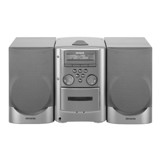
- Page 1 XR-M161 HS(S),K(S) SERVICE MANUAL BASIC TAPE MECHANISM : 2ZM-1 YR12NC COMPACT DISC STEREO SYSTEM BASIC CD MECHANISM : DA11T3C (XR-M161HS) BASIC CD MECHANISM : KSM213CDM (XR-M161K) SYSTEM CD–CASSEIVER SPEAKER XR-M161HS(S) CX-SLM161 SX-SLM161 XR-M161K(S) S/M Code No. 09-014-355-2N2...
-
Page 2: Table Of Contents
TABLE OF CONTENTS SPECIFICATIONS .............................. 3 ACCESSORIES/PACKAGE LIST-1/1 ......................... 4 PROTECTION OF EYES FROM LASER BEAM DURING SERVICING ............5 Precaution to replace Optical block (SF-P101NR, KSS-213C) ................6 ELECTRICAL MAIN PARTS LIST ......................... 7-12 TRANSISTOR ILLUSTRATION-1/1 ........................13 WIRING-1/3 (MAIN : K MODEL) ........................14 WIRING-2/3 (MAIN : HS MODEL) ........................ -
Page 3: Specifications
SPECIFICATIONS (K MODEL) • Design and specifications are subject to change without notice (HS MODEL) • Design and specifications are subject to change without notice... -
Page 4: Accessories/Package List-1/1
ACCESSORIES/PACKAGE LIST-1/1 REF. NO PART NO. KANRI DESCRIPTION 1 8B-CLA-931-010 IB,HS(K)B<161HSSC> 1 8B-CLB-905-110 IB,K(E)B<161KSC> 2 8A-CLB-961-110 RC UNIT,RC-AAT11 3 87-A90-030-010 ANT,LOOP AM-NC C 4 87-043-115-010 ANT,FEEDER FM<161HSSC> 5 87-A90-118-010 ANT,WIRE FM (Z)<161KSC> 6 87-099-726-010 PLUG,ADPTR CONV(K)<161KSC> 7 87-A91-017-010 PLUG,CONVERSION JT-0476<161HSSC>... -
Page 5: Protection Of Eyes From Laser Beam During Servicing
PROTECTION OF EYES FROM LASER BEAM DURING SERVICING This set employs laser. Therefore, be sure to follow carefully the CAUTION instructions below when servicing. Use of controls or adjustments or performance of procedures other than those specified herein may result in hazardous WARNING! radiation exposure. -
Page 6: Precaution To Replace Optical Block (Sf-P101Nr, Kss-213C)
Precaution to replace Optical block (SF-P101NR, KSS-213C) PICK-UP Assy PWB Body or clothes electrostatic potential could ruin (SF-P101NR) laser diode in the optical block. Be sure ground body and workbench, and use care the clothes do not touch the diode. 1) After the connection, remove solder shown in the right figure. -
Page 7: Electrical Main Parts List
CAP,E 1-50 M 11L SME 89-109-521-080 TR,2SA952K C141 87-010-405-080 CAP,E 10-50 M 11L SME C142 87-010-405-080 CAP,E 10-50 M 11L SME 87-A30-492-080 TR 2SC5343G [AUK] [AIWA] 87-A30-091-080 FET,2SJ460 C143 87-010-405-080 CAP,E 10-50 M 11L SME 87-026-218-080 TR,DTC144ES C144 87-010-405-080 CAP,E 10-50 M 11L SME... - Page 8 CAP,E 4.7-50 M 11L SME FC102 87-033-213-080 FUSE CLAMP,PFC5000 C703 87-A12-310-080 C-CAP, U 0.01UF-50V K X7R FFE801 A8-8ZA-192-070 8ZA-1 FEUNC ( FM:12V) [AIWA] C704 87-A12-310-080 C-CAP, U 0.01UF-50V K X7R J101 8A-CLA-624-010 JACK,PIN 3P AUX C709 87-012-195-080 C-CAP,U 100P-50 J CH...
- Page 9 ELECTRICAL MAIN PARTS LIST-3/6 REF. NO PART NO. KANRI DESCRIPTION REF. NO PART NO. KANRI DESCRIPTION C131 87-A12-310-080 C-CAP, U 0.01UF-50V K X7R C342 87-010-318-080 C-CAP,S 47P-50 J CH GRM C132 87-A12-310-080 C-CAP, U 0.01UF-50V K X7R C345 87-012-272-080 C-CAP, U 680P-50V K X7R C133 87-A12-310-080 C-CAP, U 0.01UF-50V K X7R...
- Page 10 ELECTRICAL MAIN PARTS LIST-4/6 REF. NO PART NO. KANRI DESCRIPTION REF. NO PART NO. KANRI DESCRIPTION C799 87-010-829-080 C-CAP,U 0.047-16 Z F C217 87-010-196-080 C-CAP,S 0.1-25 Z F C2012 C812 87-A12-310-080 C-CAP, U 0.01UF-50V K X7R C218 87-010-405-080 CAP,E 10-50 M 11L SME C814 87-A12-310-080 C-CAP, U 0.01UF-50V K X7R...
- Page 11 ELECTRICAL MAIN PARTS LIST-5/6 REF. NO PART NO. KANRI DESCRIPTION REF. NO PART NO. KANRI DESCRIPTION C439 87-010-178-080 C-CAP,S 1000P-50 K B C2012 CN402 87-A60-670-010 CONN,6P H 2MM JMT C441 87-010-197-080 C-CAP,S 0.01-25 K B C2012 CN403 87-A60-619-010 CONN,2P V 2MM JMT C442 87-010-313-080 C-CAP,S 18P-50 J CH GRM<161 HSSC>...
- Page 12 ELECTRICAL MAIN PARTS LIST-6/6 • Regarding connectors, they are not stocked as they are not the initial order items. The connectors are available after they are supplied from connector manufacturers upon the order is received. CHIP RESISTOR PART CODE Chip Resistor Part Coding Figure Resistor Code Value of resistor...
-
Page 13: Transistor Illustration-1/1
TRANSISTOR ILLUSTRATION-1/1 E C B E C B E C B E C B 2SC2714 2SA1296 2SA933 2SK543 DTC124XS 2SD1381 2SD1306 KTC3198 DTC343TS 2SC2001 DTC114TK 2SA1993F 2SC4115SR DTC143TK DTC144ES 2SA1979 DTC144EK 2SC3331 2SD1858TV RT1P141C 2SA952 PT1P144C DTC124XK B C E S D G E B C B C E... -
Page 14: Wiring-1/3 (Main : K Model)
WIRING-1/3 (MAIN : K MODEL) MAIN C.B (K MODEL) R954 C761 L781 R821 R169 C775 FFE801 Q111 L772 C779 J801 C829 C828 R776 R787 ANTENNA R822 L771 R775 R772 C777 C768 C824 C949 L104 TC942 R771 L941 R826 C825 C812 C773 L942 R948... -
Page 15: Wiring-2/3 (Main : Hs Model)
WIRING-2/3 (MAIN : HS MODEL) MAIN C.B (HS MODEL) C777 C778 C775 C779 R169 Q111 R821 FFE801 L772 C828 C829 R840 L771 C768 R836 R822 R772 J801 C812 C774 R962 R743 ANTENNA R792 C769 C765 R771 CF801 C963 C820 R765 L773 L774 R760... -
Page 16: Schematic Diagram-1/5 (Main 1/2)
SCHEMATIC DIAGRAM-1/5 (MAIN 1/2) MAIN C.B (1/2) TO MAIN C.B (2/2) R139 8.2K R168 R140 K : 1.8k 8.2K HS : 3.3k SUPER INV. WOOFER IC102 FUNCTION SWITCH PHONES R157 REC/PB SW R133 1.2k C174 K : 470 HS : 390 R122 R121 Q101,102... -
Page 17: Schematic Diagram-2/5 (Main 2/2 : K Model)
SCHEMATIC DIAGRAM-2/5 (MAIN 2/2 : K MODEL) MAIN C. B (2/2) (K MODEL) BAND Q805 6ZA-1 YFEENC IF AMP DC BAL. MW IF ADJ. ADJ. TUNER ON/OFF SWITCH ANTENNA FM 75 (COAXTAL) MW/LW LOOP MW RF AMP. TM-BASE PLL-CE BAND SW AM OSC COIL FM/MW IF AM ANT COIL... -
Page 18: Schematic Diagram-3/5 (Main 2/2 : Hs Model)
SCHEMATIC DIAGRAM-3/5 (MAIN 2/2 : HS MODEL) MAIN C.B (2/2) BAND SW (HS MODEL) FFE801 8ZA-1 FEUNC DC BAL. ADJ. 10.7MHz Q711 TUNER 10.7MHz Q805 ON/OFF 2SC27140 SWITCH IF AMP ANTENNA AM IF ADJ. LOOP AM OSC COIL AM ANT COIL FM/AM IF SYSTEM TRACKING... -
Page 19: Wiring-3/3 (Front)
WIRING-3/3 (FRONT) HS MODEL K MODEL MOTOR C.B MOTOR C.B (SLED MOTOR) FRONT C.B (INSIDE LIMIT SW) IC202 TO MAIN C.B CN101 REMOTE (SPINDLE MOTOR) SENSSOR S219 S205 IC202 POWER TIMER/SLEEP CN201 R228 FB201 CD C.B C218 R209 R210 C205 R251 R247 C202... -
Page 20: Schematic Diagram-4/5 (Front)
SCHEMATIC DIAGRAM-4/5 (FRONT) FRONT C. B REG. LED C. B LCD201 ZCL-8 CN204 D941-949 SLR-342 MGT32 (LCD BACK LIGHT) IC201 D-SW LC867248A-5V96 SYSTEM CONTROL FB201 9.1k SIGNAL : BEAT SW : PB/FM Q204-207 RESET REC/PLAY SW -20-... -
Page 21: Schematic Diagram-5/5 (Cd : Hs Model)
SCHEMATIC DIAGRAM-5/5 (CD : HS MODEL) CD C.B (HS MODEL) LD DRIVE INV. N.C. CD MECHANISM (DA11T3C):161HS OPTICAL PICK UP (SF-P101NR):161HS Q491,492 8V REG. MOTOR C.B PIN3 TAPE MECHANISM (2/2) (2ZM-1 YR12NC) B+ MOT REC A REC B CRD1 CNA203 SIGNAL : PB DN6851... -
Page 22: Schematic Diagram-5/5 (Cd : K Model)
SCHEMATIC DIAGRAM-5/5 (CD : K MODEL) CD C.B (K MODEL) LD DRIVE INV. N.C. CD MECHANISM (KSM213CDM):161K OPTICAL PICK UP (KSS-213C):161K Q491,492 8V REG. MOTOR C.B PIN3 TAPE MECHANISM (2/2) (2ZM-1 YR12NC) B+ MOT REC A REC B CRD1 CNA203 SIGNAL : PB DN6851... -
Page 23: Fl (Zcl-8) Grid Assignment/Anode Connection-1/1
FL (ZCL-8) GRID ASSIGNMENT/ANODE CONNECTION-1/1 -22-... -
Page 24: Electrical Adjustment
ELECTRICAL ADJUSTMENT-1/13 (K MODEL) B AL.ADJ. TP2:Rch OUT TP4,5:DC BAL. TP3:Lch OUT TP7:MW IF REC BIAS ADJ. POINT TP9:REC BAIS TEST POINT HEAD PHONE -23-... -
Page 25: Electrical Adjustment
ELECTRICAL ADJUSTMENT-2/13 (K MODEL) DECK ADJUSTMENT DECK C.B. TAPE SPEED ADJ. HEAD AZIMUTH ADJ. 1. TAPE SPEED ADJUSTMENT Requirements • Measuring equipments : wow-flutter meter (frequency counter ) WOW&FLUTTER METER Test Tape : TTA-100 (3KHz) Test point : HP OUT Adjustment point : SFR1 INPUT HP OUT... - Page 26 ELECTRICAL ADJUSTMENT-3/13 (K MODEL) 4. REC. BIAS FREQUENCY ADJUSTMENT Requirement FREQUENCY COUNTER • Measuring equipment: frequency counter Test point : TP9 Adjustment point : L301 1) Connect the TP9 to the frequency counter. 2) Set the recording condition to the main unit. 3) Adjust the L301 until it becomes 85KHz±5KHz.
- Page 27 ELECTRICAL ADJUSTMENT-4/13 (K MODEL) TUNER ADJUSTMENT 1. VT ADJUSTMENT (LW) Requirement DIGITAL MULTIMETER • Measuring equipment : Digital multi-meter Test point : TP1(FFE801 4pin),GND Adjustment point : L942 (1) Adjust the reception frequency of the main unit to 290KHz. (2) Adjust L942 until the test point voltage (VT) is 5.5V±0.1V. (3) Adjust the reception frequency of the main unit to 144KHz.
- Page 28 ELECTRICAL ADJUSTMENT-5/13 (K MODEL) <MW / LW ADJUSTMENT> For MW / LW adjustment, do wiring and connection as in the following. 60cm Standerd Signal Generaor Connect to the respective measuring equipment Fig. 2 5. IF ADJUSTMENT (MW) OSCILLOSCOPE Requirement • Measuring equipment : Oscilloscope or Millivoltmeter Test point : TP7 (IC771 24pin), GND Adjustment point : L772...
- Page 29 ELECTRICAL ADJUSTMENT-6/13 (K MODEL) <FM ADJUSTMENT> For adjusting FM, do wiring function and connection as in the following. Standerd Signal Generaor Connect to the respective measuring equipment Fig. 1 8. TRACKING CHECK AC MILLIVOLTMETER Requirement • Measuring equipment : millivoltmeter Test point : TP2, TP3, GND (1) Adjust the S.S.G.
- Page 30 ELECTRICAL ADJUSTMENT-7/13 (HS MODEL) BAL.ADJ. TP2:Rch OUT TP4,5:DC BAL. TP3:Lch OUT TP7:AM IF REC BIAS ADJ. POINT TP9:REC BAIS TEST POINT HEAD PHONE -29-...
- Page 31 ELECTRICAL ADJUSTMENT-8/13 (HS MODEL) DECK ADJUSTMENT DECK C.B. TAPE SPEED ADJ. HEAD AZIMUTH ADJ. 1. TAPE SPEED ADJUSTMENT Requirements WOW&FLUTTER METER • Measuring equipments : wow-flutter meter (frequency counter ) Test Tape : TTA-100 (3KHz) INPUT Test point : HP OUT Adjustment point : SFR1 HP OUT 1) Connect HP OUT to the Wow - flutter meter.
- Page 32 ELECTRICAL ADJUSTMENT-9/13 (HS MODEL) 4. REC. BIAS FREQUENCY ADJUSTMENT Requirement FREQUENCY COUNTER • Measuring equipment : frequency counter Test point : TP9 Adjustment point : L301 1) Connect the TP9 to the frequency counter. 2) Set the recording condition to the main unit. 3) Adjust the L301 until it becomes 85KHz±5KHz.
- Page 33 ELECTRICAL ADJUSTMENT-10/13 (HS MODEL) TUNER ADJUSTMENT 1. VT ADJUSTMENT (AM) Requirement DIGITAL MULTIMETER • Measuring equipment : Digital multi-meter Test point : TP1(FFE801 4pin),GND Adjustment point : L773 (1) Adjust the reception frequency of the main unit to 1602KHz. (2) Adjust L773 until the test point voltage (VT) is 8.5V±0.5V. (3) Adjust the reception frequency of the main unit to 531KHz.
- Page 34 ELECTRICAL ADJUSTMENT-11/13 (HS MODEL) 5. TRACKING ADJUSTMENT AC MILLIVOLTMETER Requirement • Measuring equipment : Millivoltmeter Test point : TP2, TP3, GND Adjustment point : L774 (1) Adjust the S.S.G. setting to 999KHz of 30% variation and reduce the output level all the way. (2) Adjust the reception frequency of the main unit to 999KHz.
- Page 35 ELECTRICAL ADJUSTMENT-12/13 CD ADJUSTMENT CD PWB PATTERN SIDE PARTS SIDE R401 R402 SFR430 IC401 Vref RF SW IC402 IC403 1 2 3 • Perform the adjustments after the main unit enters the test mode. • Place the CD mechanism on level ground. •...
- Page 36 ELECTRICAL ADJUSTMENT-13/13 3. JITTER CHECK OSCILLOSCOPE 1) While oscilloscope is kept connected in the same test point as in step2. RF WAVEFORM CHECK, connect the output terminal of an oscilloscope to the JITTER METER input terminal of the jitter meter. OUTPUT INPUT 2) Set the VOLT range selector of oscilloscope to 500mV range or below.
-
Page 37: Cd Test Mode
CD TEST MODE-1/1 1. How to Start the CD Test Mode While pressing the CD FUNCTION button, insert the AC plug to the power outlet. When the test mode started, all lights on the display are lit. 2. How to Exit the CD Test Mode Press the POWER button or press the other FUNCTION buttons or disconnect the AC plug. -
Page 38: Ic Block Diagram-1/2
IC BLOCK DIAGRAM-1/2 IC, LA1837NL IC, LA6541D -37-... -
Page 39: Ic Block Diagram-2/2
IC BLOCK DIAGRAM-2/2 IC, M62495AFP AUTO RESET IC, LC72131D -38-... - Page 40 IC DESCRIPTION-1/3 (LA9241ML)-1/2 Pin No. Pin Name Description Pin to which external pickup photo diode is connected. RF signal is created by adding with the FIN2 FIN1 pin signal. FE signal is created by subtracting from the FIN1 pin signal. FIN1 Pin to which external pickup photo diode is connected.
- Page 41 IC DESCRIPTION-1/3 (LA9241ML)-2/2 Pin No. Pin Name Description Pin from which TES signal is output to DSP. “High Frequency Level” is used to judge whether the main beam position is on top of bit or on top of mirror. SLOF Sled servo off control input pin.
- Page 42 IC DESCRIPTION-2/3 (LC78622NE)-1/2 Pin No. Pin Name Description DEFI Defect sense signal (DEF) input pin. (Connect to 0V when not used) Test signal input pin with built-in pull-down resistor. Be sure to connect to 0V. Phase comparator output pin to control external VCO. VVSS —...
- Page 43 IC DESCRIPTION-2/3 (LC78622NE)-2/2 Pin No. Pin Name Description XVDD — Crystal oscillator power supply pin. XOUT Pin to which external 16.9344 MHz crystal oscillator is connected. XVSS — Crystal oscillator GND pin. Be sure to connect to 0V. SBSY Subcode block sync signal output pin. (Not connected) EFLG C1, C2, single and dual correction monitoring pin.
- Page 44 IC DESCRIPTION-3/3 (LC867248A-5V96)-1/2 Pin No. Pin Name Description O-SCONTM M62495AFP control. Open drain output. O-SCONTL O-TUDI Tuner data output. CMOS output. I-TUDO Tuner data input. Open drain input. O-TUCL Tuner clock output. CMOS output. O-COIN CD control. CMOS output. I-SQOUT CD control.
- Page 45 IC DESCRIPTION-3/3 (LC867248A-5V96)-2/2 Pin No. Pin Name Description 83-86 COM0-COM3 LCD common output. I-INIT Initial setting input. ______ I-AC/DC AC/DC detection.“H” during AC. COMS input. VSS3 — GND. VDD3 — — Not used. O-TUCE Tuner chip enable output. CMOS output . O-CD-ON “H”...
-
Page 46: Mechanical Exploded View-1/1
MECHANICAL EXPLODED VIEW-1/1 KSM213 HT-SINK PLATE,SHIELD PT 2ZM-1YR12NC CHAS, MAIN -45-... -
Page 47: Mechanical Parts List-1/1
MECHANICAL PARTS LIST-1/1 REF. NO PART NO. KANRI DESCRIPTION REF. NO PART NO. KANRI DESCRIPTION 1 88-CL5-202-010 HLDR,CASS LOCKE R 28 8B-CLA-022-010 CABI,REAR H<161HSSC> 2 8Z-CL8-209-010 SPR-T,CASS 29 8Z-CL8-201-010 GUIDE,LCD 3 8B-CLA-004-010 BOX,CASS<161HSSC> 30 8B-CLA-005-010 KEY,FUNC<161HSSC> 3 8B-CLL-009-010 BOX,CASS E<161KSC> 30 8B-CLL-010-010 KEY,FUNC E<161KSC>... -
Page 48: Color Name Table
COLOR NAME TABLE Basic color symbol Color Basic color symbol Color Basic color symbol Color Black Cream Orange Green Gray Blue Transparent Blue Gold Pink Silver Titan Silver Brown Violet White Transparent White Yellow Transparent Yellow Metallic Blue Light Blue Transparent Green Dark Blue Transparent Orange... -
Page 49: Tape Mechanism Exploded View-1/1 (2Zm-1 Yr12Nc)
TAPE MECHANISM EXPLODED VIEW-1/1 (2ZM-1 YR12NC) HLDR, MOTOR PLATE, SHLD MOTOR HLDR, IC -48-... -
Page 50: Tape Mechanism Parts List-1/1 (2Zm-1 Yr12Nc)
TAPE MECHANISM PARTS LIST-1/1 (2ZM-1 YR12NC) REF. NO PART NO. KANRI DESCRIPTION REF. NO PART NO. KANRI DESCRIPTION 1 82-ZM1-247-210 PULLEY,MOTOR 31 82-ZM1-240-110 LVR,REC(*) 2 82-ZM1-354-010 BELT,SBU MAIN2 EPDM 32 82-ZM1-259-210 SPR-T,PINCH R 3 82-ZM1-234-310 FLY-WHL ASSY,L 33 82-ZM1-257-010 SPR-T,CAS 4 82-ZM1-226-010 GEAR,REW 34 82-ZM1-285-410... -
Page 51: Cd Mechanism Exploded View-1/2 (Da-11T3C)
CD MECHANISM EXPLODED VIEW-1/2 (DA-11T3C) MOTOR C.B PIN 3 -50-... -
Page 52: Cd Mechanism Parts List-1/2 (Da-11T3C)
CD MECHANISM PARTS LIST-1/2 (DA-11T3C) REF. NO PART NO. KANRI DESCRIPTION 1 M8-ZZK-E90-070 DA11T3C 2 S2-121-A28-400 COVER GEAR 3 S2-511-A21-000 GEAR MIDDLE 4 S2-511-A21-100 GEAR,DRIVE A S1-PN2-03R-OSE SCR PAN PCS 2-3 -51-... -
Page 53: Cd Mechanism Exploded View-2/2 (Ksm-213Cdm)
CD MECHANISM EXPLODED VIEW-2/2 (KSM-213CDM) COVER SPINDLE MOTOR (M3) (M2) MOTOR C.B -52-... -
Page 54: Cd Mechanism Parts List-2/2 (Ksm-213Cdm)
CD MECHANISM PARTS LIST-2/2 (KSM-213CDM) REF. NO PART NO. KANRI DESCRIPTION 1 9X-262-620-210 MOTOR CHASSIS ASSY 2 92-626-907-010 GEAR(A) 3 87-A90-468-010 PICK UP KSS-213C 4 92-626-908-010 SHAFT SLED 5 92-627-003-020 GEAR(B)(RP) A 97-621-255-150 SCREW+P2-3 -53-... -
Page 55: Speaker Disassembly Instructions-1/1
SPEAKER DISASSEMBLY INSTRUCTIONS-1/1 Type.4 Type.1 TOOLS Insert a flat-bladed screwdriver into the position indicated by the arrows 1 Plastic head hammer and remove the panel. Remove the screws of each speaker unit andthen 2 (-) flat head screwdriver remove the speaker units. 3 Cut chisel How to Remove the PANEL, FR Type.2... -
Page 56: Speaker Parts List-1/1
SPEAKER PARTS LIST-1/1 REF. NO PART NO. KANRI DESCRIPTION 1 8B-CPL-005-010 CABI, 2 8A-CLL-409-010 CORD,SP 3 8B-CPL-002-010 GRILLE,FRAME ASSY<161YJMN> 3 8B-CPL-007-010 GRILLE,FRAME ASSY G<161YJ1MN> 4 8B-CPL-001-010 PANEL,SP<161YJMN> 4 8B-CPL-009-010 PANEL,SP G<161YJ1MN> 5 8A-CLL-408-010 SPKR, 100 4 OHMS *NOTE 161HS SX-SLM161 YJMN 161K SX-SLM161 YJ1MN -55-... - Page 57 2–11, IKENOHATA 1–CHOME, TAITO-KU, TOKYO 110-8710, JAPAN TEL:03 (3827) 3111 H251941 Printed in Singapore...
Need help?
Do you have a question about the XR-M161HS(S) and is the answer not in the manual?
Questions and answers