Table of Contents
Advertisement
MITSUBISHI MOTORS
AM / FM-ST (MW / LW / FM-ST) ELECTRONIC TUNING RADIO,
For the mecha part, please refer to the service manual of
FEATURES and SPECIFICATIONS .................. 2
OPERATION .................................................. 3~5
RADIO DATA SYSTEM ...................................... 6
REAR VIEW and CONNECTORS ..................... 7
BLOCK DIAGRAM .............................................. 8
SYSTEM CONFIGURATION .............................. 8
DISASSEMBLING PROCEDURES .............. 9~11
EXPLODED VIEW and PARTS LIST ............... 12
MITSUBISHI ELECTRIC CORP. SANDA WORKS
SE018107093E
SERVICE MANUAL
6 DISC CD CHANGER
DY-6MW7U53-2
Model :
PART No.
MELCO CODE : 34U241
CONTENTS
Your company internal use only
: 8701A237
CDX3(955050).
IC EXPLANATION ...................................... 13~16
ELECTRICAL PARTS LIST ......................... 17,18
PCB-MAIN ............................................... 19,20
PCB-MAIN .............................................. 21~25
............................................... 26,27
WAVEFORM ............................................... 28,29
Copyright (c) Mitsubishi Electric Corporation
DY-6MW7U53-2
2007 SEP.
Advertisement
Table of Contents

Related Manuals for Mitsubishi DY-6MW7U53-2


Summary of Contents for Mitsubishi DY-6MW7U53-2
-
Page 1: Table Of Contents
BLOCK DIAGRAM ..........8 SCHEMATIC DIAGRAM SYSTEM CONFIGURATION ......8 PCB-MAIN ..........21~25 DISASSEMBLING PROCEDURES ....9~11 VOLTAGE ..........26,27 EXPLODED VIEW and PARTS LIST ....12 WAVEFORM ..........28,29 MITSUBISHI ELECTRIC CORP. SANDA WORKS SE018107093E Copyright (c) Mitsubishi Electric Corporation... -
Page 2: Features And Specifications
FEATURES and SPECIFICATIONS FEATURES Others Sounding the beep as the long pushing button. Radio Interrupting the telephone voice. Manual preset function / Store 6 AM(MW) stations. Checking the speaker connection. Manual preset function / Store some FM stations. (EU : 18 Operated the steering remote control. -
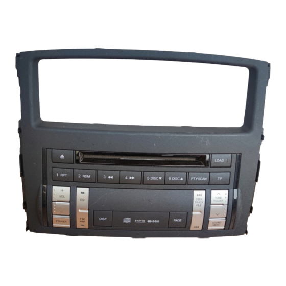
Page 3: Operation
OPERATION < SW-6ME7BLN, SW-6ME7BLP > (for EU) Radio Mode Preset Button ch1~6 Program Type/ Scan Button Traffic Program Button Volume Up Button Tune Up/Down Volume Down Button Button Power Button FM/AM Changing Button Auto Tune Up/Down Button CD Changer Mode CD Insertion Slot Fast Forward Button Disc Up/Down Button... - Page 4 < SW-6MA7BRN, SW-6MA7BRP > (for AUS) Radio Mode Preset Button ch1~6 Auto Program Button Scan Button Volume Up Button Tune Up/Down Volume Down Button Button Power Button FM/AM Changing Button Auto Tune Up/Down Button CD Changer Mode CD Insertion Slot Fast Forward Button Disc Up/Down Button (only when using 6CD-...
- Page 5 < SW-6MX7BLN, SW-6MX7BLP > (for CHINA, GCC and ROW) Radio Mode Preset Button ch1~6 Auto Program Button Scan Button Volume Up Button Tune Up/Down Volume Down Button Button Power Button FM/AM Changing Button Auto Tune Up/Down Button CD Changer Mode CD Insertion Slot Fast Forward Button Disc Up/Down Button...
-
Page 6: Radio Data System
RADIO DATA SYSTEM (EU only) It automatically identifies RDS station by detecting RDS signal 7) CT (Clock Time) transmitted from UKW stations. Some RDS station broadcast time signal. When CT function is ON, CT indicator appear in display, 1) PS (Program Service) Name and such a station is being received, this function automati- At the statement of RDS data receiving PS Name (station cally adjusts clock to correct local time. -
Page 7: Rear View And Connectors
REAR VIEW and CONNECTORS Main Antenna Socket Panel / Amp Power Supply, Speaker and AUX Input 20P Connector (P901) 18P Connector (P801) 9 8 7 6 5 4 3 14 13 9 8 7 6 5 4 3 14 13 Panel / Amp and AUX Input 18P Connector (P801) NAME NAME... -
Page 8: Block Diagram
CD L,R 5 Line <J700> Panel/Display display / switch SYSTEM CONFIGURATION MAIN ANTENNA VEHICLE/ SEPARATE AMPLIFIER AUDIO UNIT REMOTE CONTROL (STEERING) DY-6MW7U53-2 ANTENNA VEHICLE SPEED PULSE SWITCH SW-6ME7BLN,etc. HANDS FREE KIT DISPLAY 8750A042 (Visteon) TO SPEAKER HARNESS SEPARATE AMPLIFIER RSES ED-310RG-PJ2,etc. -
Page 9: Disassembling Procedures
DISASSEMBLING PROCEDURES 1. Removal of COVER (See Fig.1) 1) Unscrew the four screws ( 1 ). 2) Remove the COVER. 4(A) COVER Fig.1 2. Removal of CDX3 (See Fig.2) 1) Unscrew the two screws ( 2 ). BRACKET-CDX3 2) Remove the CDX3 and FLAT-CABLE 18P. 2(A) 3) Unscrew the two screws ( 3 ). - Page 10 3. Removal of HEAT-SINK (See Fig.3) 1) Unscrew the four screws ( 5 ). 2) Remove the HEAT-SINK. 4(C) HEAT-SINK Fig.3 4. Removal of CHASSIS (See Fig.4) 1) Unscrew the three screws ( 6 ). 2) Remove the CHASSIS-F. 3) Unscrew the two screws ( 7 ). 4) Remove the CHASSIS-L.
- Page 11 5. Removal of PCB-MAIN (See Fig.5) 3(A) 1) Unscrew the four screws ( 10 ). 2) Unlatch the five hooks ( a ). 3) Remove the PCB-MAIN. PCB-MAIN Fig.5...
-
Page 12: Exploded View And Parts List
M013 643L015O3 SHEET M016 940L10114 CDX3(955050) M019 591K61510 BRACKET-CASE M020 593L83310 BRACKET-CDX3 M023 M021 642K14611 SHEET-CD M020 M022 246L229O6 FLAT-CABLE 18P M023 943M242O1 NAME-CARD(DY-6MW7U53-2) 653P11046 SCREW-S-PAN 3X6 653P11048 SCREW-S-PAN 3X10 653P11049 SCREW-S-PAN 3X12 669L057O1 SCREW-TAP 3X6 M019 M022 M003 M016 M021... -
Page 13: Ic Explanation
IC EXPLANATION IC200 SN74LVTH244APWR IC8C1 SN74AHCT244PWR IC961,981 LF33ABPT CURRENT LIMIT START REFERENCE INHIBIT INHIBIT VOLTAGE DRIVER ERROR CONTROL AMPLIFIER DUMP PROTECTION TERM. PROTECTION IC8A1 MM1185AFFE 2.4 A typ 1 A typ 0.48 A typ 0.1V RESET 1.25V typ 0.2V Pulse Generator... - Page 14 IC8N1 M24C02-WMN6TP PROGRAM TIMER CHARGE PUMP EEPROM ARRAY 64 LATCH PREDEC 8-BIT COUNTER ADDRESS CLOCK SENSE RESISTOR RESISTOR 1 A0 2 A1 3 A2 OUTPUT LOGIC START STOP START / STOP . LOGIC TEST IC21G,305,405 NJM4580V 2,6 INPUT- 3,5 INPUT+ 1,7 OUTPUT...
- Page 15 IC202 AK7730AVT AINL+ AINL+ AINL- AINL- AINR+ AINR+ AINR- AINR- VREFH VREFH VREFL VREFL VCOM VCOM SDATA SWQA SWQ4 SDOUT4 JX0/SDIN4A SWQ3 SDIN3/JX1 SDOUT3 SWQ2 SDIN2/JX2 SDOUT2 SWQ1 SDIN1 SDOUT1 SWIA SDIN4 SDOUT4 SDOUT3 SDIN3 SDIN2 SDOUT2 SDIN1 SDOUT1 SWJX0 SCLK SCLK SWJX1...
- Page 16 IC204 SAA7709H/N103 Level WSPLL CHANNEL1 CHANNEL2 INPUT Left SELECT Right BLOCK Left STEREO DECODER NOISE Right Pilot Filter IIC & SPDIF 11.2896MHz DEMOD DECOD 45 44 27 29 28 25 24 62 65 63 64 58 57 PinNo Pin Name PinNo Pin Name PinNo...
-
Page 17: Electrical Parts List
ELECTRICAL PARTS LIST < CHIP PARTS (RESISTORS & CAPACITORS) > Part No. Part No. 103L19XOX 2.0mm 141L06XOX 2.0mm 141L16XOX 1.6mm 103L24XOX 3.2mm 103L29XOX 1.6mm 141L18XOX 1.6mm SOLDERING PART 103P50XOX 1.6mm 141P17XOX 3.2mm Ref. No. Part No. Description Ref. No. Part No. Description RN202,8C1 109L034O6 R-NETWORK-CHIP... - Page 18 Ref. No. Part No. Description Ref. No. Part No. Description D101 264L062O1 DIODE-CHIP 1SV234 COILS D9M1 264P516O1 DIODE-CHIP S3D6600 L9M1 351P11610 COIL-CHOKE D8L3 264P582O7 DIODE-Z-CHIP MA8043H 351P032O1 COIL-CHOKE-CHIP D932 264L067O3 DIODE-Z-CHIP MA8051M L101,9A1 351P081O6 COIL-CHOKE-CHIP D911,9A2 264L067O4 DIODE-Z-CHIP MA8056M L221~231,etc. 351P095O4 COIL-CHOKE-CHIP D952 264P583O8 DIODE-Z-CHIP MA8062M...
-
Page 19: Parts Layout On Printed Circuit Board
PARTS LAYOUT ON PRINTED CIRCUIT BOARD MODEL : DY-6MW7U53-2 (PARTS SIDE) PCB-MAIN... -
Page 20: Pcb-Main
PARTS LAYOUT ON PRINTED CIRCUIT BOARD MODEL : DY-6MW7U53-2 (PATTERN SIDE) PCB-MAIN TO CDX3... -
Page 21: Pcb-Main
SCHEMATIC DIAGRAM PCB-MAIN MODEL : DY-6MW7U53-2 Vol.1 Vol.3 Vol.4 Vol.2... -
Page 22: Schematic Diagram Pcb-Main
SCHEMATIC DIAGRAM PCB-MAIN MODEL : DY-6MW7U53-2 Vol.1... - Page 23 SCHEMATIC DIAGRAM PCB-MAIN MODEL : DY-6MW7U53-2 Vol.2...
- Page 24 SCHEMATIC DIAGRAM PCB-MAIN MODEL : DY-6MW7U53-2 Vol.3...
- Page 25 SCHEMATIC DIAGRAM PCB-MAIN MODEL : DY-6MW7U53-2 Vol.4...
-
Page 26: Voltage
VOLTAGE MODEL : DY-6MW7U53-2 (Pin numbers are as measurement points.) 1. Audio -COM 2. CDSP IC800 PCB-MAIN IC204 PCB-MAIN FM 98.1MHz,30.0%MOD,VOL MIN BATT,ACC 13.2V Voltage [V] Voltage [V] Pin Name Function Pin Name Function Pin Name Voltage [V] Pin Name... -
Page 27: Voltage
3. SUB DSP 4. POWER-IC IC202 PCB-MAIN IC307 PCB-MAIN FM 98.1MHz,30.0%MOD,VOL MIN FM 98.1MHz,30.0%MOD,VOL MIN BATT,ACC 13.2V BATT,ACC 13.2V Pin Name Voltage [V] Pin Name Voltage [V] 1 EESEL 2 JX0 STBY 11.7 3 SDIN3 PGND 4 SDIN2 5 SDIN1 0.0/3.3 6 CKS1 7 BVSS... -
Page 28: Waveform
WAVEFORM MODEL : DY-6MW7U53-2 (Pin numbers are as measurement points.) 1. -COM 3. -COM 5. CD Connector IC800 IC800 J700 PCB-MAIN PCB-MAIN PCB-MAIN CH1=27PIN(SCL, 5.0Vpp) CH1=33PIN(AMP/RSES(UART) PC-TXD, 5.0Vpp) CH1=14PIN(D-STM, 5.0Vpp) CH2=28PIN(SDA, 5.0Vpp) CH2=34PIN(AMP/RSES(UART) PC-RXD, 5.0Vpp) CH2=12PIN(D-MTS, 4.2Vpp) CH3=13PIN(SCK, 5.0Vpp) Time axis : 20us/div Time axis : 200us/div CH4=15PIN(MTS, 5.0Vpp) - Page 29 6. -COM IC800 PCB-MAIN CH1=11PIN(XOUT, 5.1Vpp) CH2=13PIN(XIN, 4.9Vpp) Time axis : 50ns/div Cycle(CH2) : 10.0MHz 7. CDSP IC204 PCB-MAIN CH1=63PIN(OSC-IN, 3.2Vpp) CH2=64PIN(OSC-OUT, 3.2Vpp) Time axis : 50ns/div Cycle(CH1) : 11.3MHz...
Need help?
Do you have a question about the DY-6MW7U53-2 and is the answer not in the manual?
Questions and answers