Sony mds-s38 Service Manual
Hide thumbs
Also See for mds-s38:
- Operating instructions manual (112 pages) ,
- Operating instructions manual (109 pages) ,
- Operating instructions manual (76 pages)
Table of Contents
Advertisement
SERVICE MANUAL
Ver 1.1 2004. 09
Sony Corporation
9-960-934-12
Audio Group
2004I02-1
Published by Sony Engineering Corporaton
© 2004.09
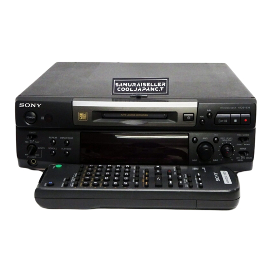
MDS-S38
Photo: Black
Model Name Using Similar Mechanism
MD Mechanism Type
Optical Pick-up Type
SPECIFICATIONS
US Model
Canadian Model
AEP Model
UK Model
E Model
MDS-S37
MDM-3B
KMS-260A/J1N
MiNi DiSC DECK
Advertisement
Table of Contents

Related Manuals for Sony mds-s38


Summary of Contents for Sony mds-s38
- Page 1 Ver 1.1 2004. 09 AEP Model UK Model E Model Photo: Black Model Name Using Similar Mechanism MDS-S37 MD Mechanism Type MDM-3B Optical Pick-up Type KMS-260A/J1N SPECIFICATIONS MiNi DiSC DECK Sony Corporation 9-960-934-12 Audio Group 2004I02-1 Published by Sony Engineering Corporaton © 2004.09...
- Page 2 REPLACE THESE COMPONENTS WITH SONY PARTS FONCTIONNEMENT. NE REMPLACER CES COMPOSANTS WHOSE PART NUMBERS APPEAR AS SHOWN IN THIS QUE PAR DES PIÈCES SONY DONT LES NUMÉROS MANUAL OR IN SUPPLEMENTS PUBLISHED BY SONY. SONT DONNÉS DANS CE MANUEL OU DANS LES SUPPLÉMENTS PUBLIÉS PAR SONY.
-
Page 3: Table Of Contents
SAFETY CHECK-OUT TABLE OF CONTENTS After correcting the original service problem, perform the follow- 1. SERVICING NOTE ............5 ing safety checks before releasing the set to the customer: Check the antenna terminals, metal trim, “metallized” knobs, screws, 2. GENERAL ................ -
Page 4: Servicing Note
SECTION 1 SERVICING NOTE JIG FOR CHECKING BD BOARD WAVEFORM The special jig (J-2501-124-A) is useful for checking the waveform of the BD board. The names of terminals and the checking items to be performed are shown as follows. I+3V : For measuring IOP (Check the deterioration of the optical pick-up laser) IOP : For measuring IOP (Check the deterioration of the optical pick-up laser) TEO : TRK error signal (Traverse adjustment) : Reference level for checking the signal... - Page 5 RETRY CAUSE DISPLAY MODE • In this test mode, the causes for retry of the unit during recording can be displayed on the fluorescent display tube. This is useful for locating the faulty part of the unit. • The data amount stored in D RAM, number of retries, and retry cause are displayed. Each is displayed in hexadecimal number. •...
- Page 6 Reading the Retry Cause Display Higher Bits Lower Bits Hexa- Hexadecimal Cause of Retry Occurring conditions decimal b7 b6 b5 b4 b3 b2 b1 b0 Binary Spindle is slow When spindle rotation is detected as slow (Not used) (Not used) When ADER was counted more than ader5 five times continuously...
-
Page 7: General
SECTION 2 GENERAL Location of Parts and Controls 18 17 POWER switch 11 REC LEVEL (ANALOG) knob Remote sensor 12 AMS knob Disc compartment 13 EDIT/NO/YES buttons § (eject) button 14 Display window 0/) (fast backward/fast forward) buttons 15 DISPLAY/CHAR button fl... - Page 8 This section is extracted from instruction manual. — 8 —...
- Page 9 — 9 —...
- Page 10 — 10 —...
- Page 11 — 11 —...
- Page 12 — 12 —...
- Page 13 — 13 —...
- Page 14 — 14 —...
- Page 15 — 15 —...
- Page 16 — 16 —...
- Page 17 — 17 —...
- Page 18 — 18 —...
- Page 19 — 19 —...
- Page 20 — 20 —...
- Page 21 — 21 —...
- Page 22 SECTION 3 DISASSEMBLY Follow the disassembly procedure in the numerical order given. Note : 3-1. FRONT PANEL 1 Connector (CN800) 5 Front panel 2 Flat type wire (23 core) 4 Three claws 3 Four screws (BVTP3x10) — 22 —...
-
Page 23: Back Panel And Main Board
3-2. BACK PANEL AND MAIN BOARD !§ Back panel !º Three screws (BVTP3x10) !¢ Main board 9 Flat type wire 8 Flat type wire (29 core) (19 core) !¡ Two screws (BVTP3x10) 4 RIVET (AEP, UK, Singapore, Hongkong) 3 Two screws !∞... -
Page 24: Bracket (T), (L) And (R)
3-3. BRACKET (T), (L) AND (R) 1 Four screws 4 Screw (BVTT2x3) (BVTT2x3) 2 Bracket (T) 3 Screw (BVTT2x3) 6 Two screws (BVTT2x3) 5 Bracket (joint) 7 Bracket (L) 9 Bracket (R) 8 Two screws (BVTT2x3) 3-4. BD BOARD 2 Flat type wire (15 core) 4 OP relay flexible board 1 Flexible board (Over write head) -
Page 25: Sub Chassis
3-5. SUB CHASSIS 1 Two step screws 2 Two step screws 3 Two insulators 4 Two insulators Part A Part A Part A 5 Sub chassis Take care so that the part A may be right position when installing. 3-6. SHUTTER ASSEMBLY 1 Stopper washer Shutter assembly Shaft (lid) -
Page 26: Over Write Head
3-7. OVER WRITE HEAD 1 Precision screw (P1.7x6) 2 Over write head — 26 —... -
Page 27: Slider Complete Assembly
3-8. SLIDER COMPLETE ASSEMBLY 3 Set the shaft of Gear (LA) to be at the claw position in the figure. claw 45° 4 Remove the slider complete assembly 1 Screw in the direction of arrow with putting (M1.7x2) 2 Retainer (gear) out of two claws. -
Page 28: Test Mode
SECTION 4 TEST MODE 4-1. PRECAUTIONS FOR USE OF TEST MODE 1 As loading related operations will be performed regardless of the test mode operations being performed, be sure to check that the disc is stopped before setting and removing it. Even if the §... - Page 29 4-5-1. Operating the Continuous Playback Mode 1. Entering the continuous playback mode 1 Set the disc in the unit. (Whichever recordable discs or discs for playback only are available.) 2 Rotate the AMS knob and display “CPLAY MODE”. 3 Press the YES button to change the display to “CPLAY IN”. 4 When access completes, the display changes to “C1 = AD = ”.
- Page 30 4-6. FUNCTIONS OF OTHER BUTTONS Function Contents fl Sets continuous playback when pressed in the STOP state. When pressed during continuous playback, the tracking servo turns ON/OFF. Stops continuous playback and continuous recording. The sled moves to the outer circumference only when this is pressed. The sled moves to the inner circumference only when this is pressed.
-
Page 31: Electrical Adjustments
SECTION 5 ELECTRICAL ADJUSTMENTS 5-1. PRECAUTIONS FOR CHECKING LASER DIODE 5-3. PRECAUTIONS FOR ADJUSTMENTS EMISSINON 1) When replacing the following parts, perform the adjustments and checks with ¬ in the order shown in the following table. To check the emission of the laser diode during adjustments, never view directly from the top as this may lose your eye-sight. - Page 32 5-6. LASER PPOWER ADJUSTMENT 5-5. TEMPERATURE COMPENSATION OFFSET Connection : ADJUTMENT Laser power Save the temperature data at that time in the non-volatile memory meter as 25 ˚C reference data. Note : 1. Usually, do not perform this adjustment. 2. Perform this adjustment in an ambient temperature of 22 ˚C to Optical pick-up 28 ˚C.
- Page 33 5-7. TRAVERSE ADJUSTMENT 11. Rotate the AMS knob until the waveform of the oscilloscope moves closer to the specified value. Connection : In this adjustment, waveform varies at intervals of approx. 2%. Oscilloscope Adjust the waveform so that the specified value is satisfied as much as possible.
- Page 34 5-8. FOCUS BIAS ADJUSTMENT 5-9. ERROR RATE CHECK 5-9-1. CD Error Rate Check Adjusting Method : 1. Load a continuously recorded disc (Refer to “5-4. Creating Con- Checking Method : tinuously Recorded Disc”.). 1. Load a check disc (MD) TDYS-1. 2.
-
Page 35: Circuit Boards Location
SECTION 6 DIAGRAMS 5-11. ADJUSTING POINTS AND CONNETING POINTS 6-1. CIRCUIT BOARDS LOCATION [BD BOARD] (SIDE A) 5 CN110 NOTE I + 3V TRANSFORMER board CN101 MAIN board SW board D101 IC192 [BD BOARD] (SIDE B) BD board PANEL board IC171 IC101 IC121... - Page 36 MDS-S38 6-2. BLOCK DIAGRAMS — BD SECTION — DIGITAL SERVO SIGNAL PROCESSOR, DIGITAL SIGNAL PROCESSOR OVER WRITE HEAD DRIVE EFM/ACIRC ENCODER/DECODER, SHOCK-PROOF MEMORY CONTROLLER, IC181 ATRAC ENCODER/DECODER, 2M-BIT DRAM IC121 SCTX XINT Q180 HR901 • Signal path OVER WRITE HEAD...
-
Page 37: Main Section
MDS-S38 DIGITAL INPUT SELECTOR BUFFER IC315 IC314 — MAIN SECTION — Tourist IC354 DIGITAL A/D, D/A CONVERTER OPTICAL 1 IC201 RV702 REC LEVEL INLM INLP IC353 ADDT EXCEPT Tourist INRP DIGITAL 4 • 5 CONVERTER DIGITAL INRM R-ch R-ch OPTICAL... - Page 45 IC101 CXA8065S IC201 CXD8607N INRP INLP LINE02 LINE1 MODULATOR MODULATOR INRM INLM – – PMUTE REFI REFO MIC1 LINE01 AVDD LVSS SW01 AVSS LVDD MUTE DECIMATION DECIMATION AVSS(LF) FILTER FILTER VOLTAGE LINE/MIC SWI1 – REFERENCE LOW CUT LOW CUT –A/D1 TEST1 FILTER FILTER...
- Page 46 IC501 LA5620 IC310 M5293L – REFERENCE VOLTAGE STBY REFERENCE ON/OFF – VOLTAGE OVERHEAT OVERCURRENT PROTECTION LIMITTER ANA5 – SYS3.3 – – 3.3V BACK – DELAY CIRCUIT P. DOWN – DELAY CIRCUIT VREF S. RESET — 64 —...
-
Page 47: Ic Pin Functions
6-10. IC PIN FUNCTIONS • IC101 RF Amplifier (CXA2523R) Pin No. Pin Name Function I-V converted RF signal I input I-V converted RF signal J input Middle point voltage (+1.5V) generation output 4 to 9 A to F Signal input from the optical pick-up detector Light amount monitor input Laser APC output APCREF... - Page 48 • IC121 Digital Signal Processor, Digital Servo Signal Processor, EFM/ACIRC Encoder/Decoder, Shock-proof Memory Controller, ATRAC Encoder/Decoder, 2M Bit DRAM (CXD2652AR) Pin No. Pin Name Function FOK signal output to the system control MNT0 (FOK) “H” is output when focus is on MNT1 (SHCK) Track jump detection signal output to the system control MNT2 (XBUSY)
- Page 49 Pin No. Pin Name Function Data input/output for DRAM D2, D3 48, 49 MVCI Clock input from an external VCO (Fixed at “L”) I (S) ASYO Playback EFM duplex signal output ASYI I (A) Playback EFM comparator slice level input AVDD +3V power supply (Analog) —...
- Page 50 Pin No. Pin Name Function Tracking servo drive PWM output (+) TFDR — +3V power supply (Digital) DVDD Focus servo drive PWM output (+) FFDR Focus servo drive PWM output (–) FRDR 176.4 kHz clock signal output (X’tal) (Not used) Sled servo drive PWM output (–) SRDR Sled servo drive PWM output (+)
- Page 51 • IC201 A/D, D/A converter (CXD8607N) Pin No. Pin Name Function INRP Rch analog (+) input INRM Rch analog (–) input REFI A/D reference voltage input (+3.2V) — +5V power supply (A/D, analog) AVss — Ground (A/D, analog) A/D analog block power down “L”: Power down —...
- Page 52 Pin No. Pin Name Function Lch PLM output 1 — +5V power supply (D/A, digital) — +5V power supply (A/D, digital) — — Ground (A/D, digital) TEST2 Test pin (Fixed at “L”) TEST3 — Ground (A/D, digital) SS1 (LF) — Not used —...
- Page 53 • IC401 System Control (RU8X11AMF-0115) Pin No. Pin Name Function Test pin. C1 is output when test mode (Not used) DAOUT 0 Test pin. ADER is output when test mode (Not used) DAOUT 1 Key input pin (D/A input) 3 to 5 KEY0 to KEY2 Detection input from the chucking-in switch “L”: Chucking CHUCK IN...
- Page 54 Pin No. Pin Name Function MNT2 Monitor 2 input from the CXD2652AR MNT3 Monitor 3 input from the CXD2652AR LED0 Drive output to the POWER ON/STANDBY display LED — Power supply ON: “H”, stand by: “L” (Not used) — Not used BUS OUT Not used —...
- Page 55 Pin No. Pin Name Function DIG-RST Reset signal output to the CXD2652AR and motor driver Reset: “L” BEEP PWM output (Not used) BEEP Reset signal output to the D/A, A/D converter Reset: “L” ADARES Not used SEL-A Digital input selection signal output SEL B Laser modulation switching signal output Playback power: “L”, stop: “H”...
- Page 56 SECTION 7 EXPLODED VIEWS NOTE: The components identified by • Hardware (# mark) list and accessories and pack- • Items marked “*” are not stocked since they are mark ! or dotted line with mark ing materials are given in the last of this parts list. seldom required for routine service.
-
Page 57: Front Panel Section
X-4948-321-1 PANEL ASSY, FRONT (SILVER)(EXCEPT JE) 2-389-320-01 CUSHION 4-951-620-01 SCREW (2.6X8), +BVTP * 62 A-4699-645-A PANEL BOARD, COMPLETE (JE) 4-962-708-11 EMBLEM (4-A), SONY * 62 A-4699-715-A PANEL BOARD, COMPLETE (AEP,UK) 4-989-520-01 KNOB (REC)(BLACK) * 62 A-4699-718-A PANEL BOARD, COMPLETE (US,CND) -
Page 58: Mechanism Deck Section (1) (Mdm-3B)
7-3. MECHANISM DECK SECTION (1) (MDM-3B) not supplied not supplied not supplied not supplied not supplied Ref. No. Part No. Description Remark Ref. No. Part No. Description Remark 4-628-167-01 SCREW, STEP X-4948-722-1 SHUTTER ASSY (SILVER) 4-987-327-01 INSULATOR 1-660-966-11 OP RELAY FLEXIBLE BOARD 4-986-959-01 WASHER, STOPPER * 207 A-4699-770-A BD BOARD, COMPLETE... -
Page 59: Mechanism Deck Section (2) (Mdm-3B)
Ver 1.1 7-4. MECHANISM DECK SECTION (2) (MDM-3B) not supplied not supplied M901 M902 M903 HR901 Les composants identifiés par The components identified by mark 0 or dotted line with mark une marque 0 sont critiques pour 0 are critical for safety. la sécurité. -
Page 60: Electrical Parts List
SECTION 8 ELECTRICAL PARTS LIST Note: • SEMICONDUCTORS • Due to standardization, replacements in the parts list The components identified by In each case, u: µ , for example: may be different from the parts specified in the mark ! or dotted line with mark uA...: µ... - Page 61 Ref. No. Part No. Description Remark Ref. No. Part No. Description Remark IC152 8-759-430-25 IC BH6511FS-E2 R137 1-216-025-00 METAL GLAZE 1/10W IC171 8-759-428-58 IC XL24C01AF-E2 R140 1-216-029-00 METAL CHIP 1/10W IC181 8-759-095-65 IC TC74ACT540FS R141 1-216-295-00 CONDUCTOR, CHIP (2012) R142 1-216-073-00 METAL CHIP 1/10W IC192...
- Page 62 MAIN Ref. No. Part No. Description Remark Ref. No. Part No. Description Remark A-4699-641-A MAIN BOARD, COMPLETE (JE) C223 1-164-159-11 CERAMIC 0.1uF C231 1-162-306-11 CERAMIC 0.01uF ************************** C234 1-126-933-11 ELECT 100uF A-4699-714-A MAIN BOARD, COMPLETE (AEP,UK) C235 1-162-207-31 CERAMIC 22PF ****************************** C236 1-162-203-31 CERAMIC...
- Page 63 MAIN Ref. No. Part No. Description Remark Ref. No. Part No. Description Remark C605 1-164-159-11 CERAMIC 0.1uF IC353 8-749-012-70 IC GP1F38R (DIGITAL IN OPTICAL 2)(JE) C606 1-164-159-11 CERAMIC 0.1uF IC353 8-749-012-70 IC GP1F38R (DIGITAL IN OPTICAL 1) C801 1-162-306-11 CERAMIC 0.01uF (EXCEPT JE) IC354...
- Page 64 MAIN Ref. No. Part No. Description Remark Ref. No. Part No. Description Remark R131 1-249-429-11 CARBON 1/4W R356 1-249-441-11 CARBON 100K 1/4W R132 1-249-429-11 CARBON 1/4W R365 1-249-441-11 CARBON 100K 1/4W R369 1-249-441-11 CARBON 100K 1/4W R134 1-249-441-11 CARBON 100K 1/4W R141 1-249-427-11 CARBON...
- Page 65 MAIN PANEL Ref. No. Part No. Description Remark Ref. No. Part No. Description Remark < SWITCH > <COIL> ! S301 1-572-675-11 SWITCH, POWER VOLTAGE CHANGE L701 1-414-142-11 INDUCTOR (VOLTAGE SELECTOR)(SP,JE) L702 1-414-142-11 INDUCTOR ! S301 1-762-764-11 SWITCH, POWER (MAIN POWER)(AEP,UK) L703 1-414-142-11 INDUCTOR <...
- Page 66 MDS-S38 PANEL TRANSFORMER Ref. No. Part No. Description Remark Ref. No. Part No. Description Remark S751 1-762-875-21 SWITCH, TACTILE (EDIT/NO) MISCELLANEOUS S752 1-762-875-21 SWITCH, TACTILE (YES) ************* S756 1-762-875-21 SWITCH, TACTILE (DISPLAY/CHAR) S761 1-762-875-21 SWITCH, TACTILE (PLAY MODE) 1-782-264-11 WIRE (FLAT TYPE)(19 CORE)
- Page 67 MDS-S38 MEMO – 85 –...
- Page 68 MDS-S38 REVISION HISTORY Clicking the version allows you to jump to the revised page. Also, clicking the version at the upper right on the revised page allows you to jump to the next revised page. Ver. Date Description of Revision 1997.04...