
Related Manuals for Toshiba 27AFX55


Summary of Contents for Toshiba 27AFX55
-
Page 1: Service Manual
FILE NO. 050-200526 (MFR’S VERSION A) SERVICE MANUAL COLOR TELEVISION 27AFX55 DOCUMENT CREATED IN JAPAN, July, 2005... -
Page 2: Servicing Notices On Checking
SERVICING NOTICES ON CHECKING 1. KEEP THE NOTICES 6. AVOID AN X-RAY As for the places which need special attentions, Safety is secured against an X-ray by consider- they are indicated with the labels or seals on the ing about the cathode-ray tube and the high cabinet, chassis and parts. -
Page 3: About Lead Free Solder (Pbf)
ABOUT LEAD FREE SOLDER (PbF) Distinction of PbF PCB: PCBs (manufactured) using lead free solder will have a PbF printing on the PCB. (Please refer to figures.) Caution: • Pb free solder has a higher melting point than standard solder; Typically the melting point is 50°F~70°F(30°C~40°C) higher. -
Page 4: Table Of Contents
TABLE OF CONTENTS SERVICING NOTICES ON CHECKING ..................A1-1 HOW TO ORDER PARTS ......................A1-1 IMPORTANT ..........................A1-1 ABOUT LEAD FREE SOLDER (PbF) ..................A1-2 TABLE OF CONTENTS ......................A2-1 GENERAL SPECIFICATIONS ....................A3-1~A3-5 DISASSEMBLY INSTRUCTIONS 1. REMOVAL OF ANODE CAP ....................B1-1 2. -
Page 5: General Specifications
GENERAL SPECIFICATIONS CRT Size / Visual Size 27 inch / 676.0mmV System CRT Type Flat Magnetic Field BV/BH +0.45G/0.18G Color System NTSC Speaker 2 Speaker Position Front Side Size 1.8 x 3.9 Inch Impedance Sound Output 5.0+5.0 W 10%(Typical) NTSC3.58+4.43 /PAL60Hz Tuning Broadcasting System System M... - Page 6 GENERAL SPECIFICATIONS On Screen Menu Display Menu Type Icon Picture Contrast Brightness Color Tint Sharpness Sound Bass Treble Balance BBE On/Off Stable Sound On/Off Surround On/Off Set Up TV/Cable Auto CH Memory Add/ Delete Option Language CH Label Favorite CH V-Chip Lock On/Off Timer...
- Page 7 GENERAL SPECIFICATIONS G-10 Remote Unit RC-LR Control Glow in Dark Remocon Format Toshiba Remocon Format Toshiba Custom Code TV:40-BF h Power Source Voltage(D.C) UM size x pcs UM-4 x 2 pcs Total Keys Keys Keys Power 100/ +10 CH Up/Cursor Up...
- Page 8 GENERAL SPECIFICATIONS G-11 Features Auto Degauss Auto Shut Off Canal+ Cable Anti-theft Rental Memory(Last CH) Memory(Last Volume) V-Chip Type Auto Search CH Allocation Just Clock Function CH Label VM Circuit Full OSD Premiere Comb Filter Lines Auto CH Memory Hotel Lock Closed Caption Stable Sound FBT Leak Test Protect...
- Page 9 Height (cm) 40 (ORION SPEC:25) Container Stuffing Sets/40' container G-17 Cabinet Material Cabinet Cabinet Front PS 94V0 DECABROM Cabinet Rear PS 94V0 DECABROM Non-Halogen Demand Eyelet Demand G-18 Environment Environmental standard requirement (by buyer) Green procurement of TOSHIBA Pb-free Phase3(Phase3A) A3-5...
-
Page 10: Disassembly Instructions
DISASSEMBLY INSTRUCTIONS 3. After one side is removed, pull in the opposite direction to 1. REMOVAL OF ANODE CAP remove the other. Read the following NOTED items before starting work. NOTE After turning the power off there might still be a potential Take care not to damage the Rubber Cap. -
Page 11: Removal And Installation Of Flat Package Ic
DISASSEMBLY INSTRUCTIONS When IC starts moving back and forth easily after REMOVAL AND INSTALLATION OF desoldering completely, pickup the corner of the IC using a FLAT PACKAGE IC tweezers and remove the IC by moving with the IC desoldering machine. (Refer to Fig. 2-3.) REMOVAL NOTE Put Masking Tape (cotton tape) around the Flat Package... - Page 12 DISASSEMBLY INSTRUCTIONS INSTALLATION When bridge-soldering between terminals and/or the soldering amount are not enough, resolder using a Thin-tip Take care of the polarity of new IC and then install the new Soldering Iron. (Refer to Fig. 2-8.) IC fitting on the printed circuit pattern. Then solder each lead on the diagonal positions of IC temporarily.
-
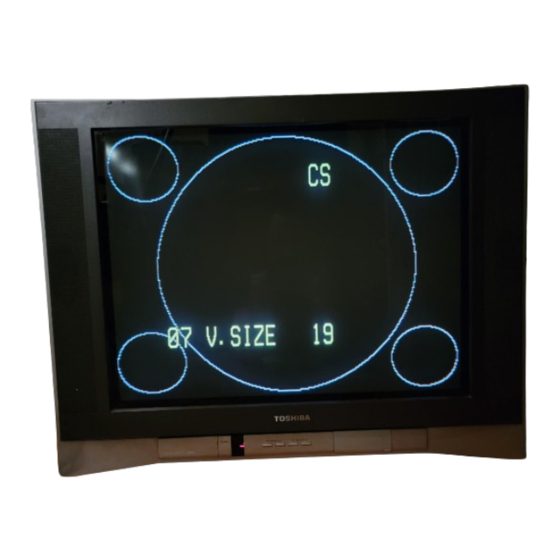
Page 13: Service Mode List
SERVICE MODE LIST This unit is provided with the following SERVICE MODES so you can repair, examine and adjust easily. To enter to the Service Mode, press both set key and remote control key for more than 2 seconds. Set Key Remocon Key Operations Releasing of V-CHIP PASSWORD and LOCK PASSWORD. -
Page 14: Electrical Adjustments
ELECTRICAL ADJUSTMENTS 1. ADJUSTMENT PROCEDURE 2. BASIC ADJUSTMENTS Read and perform these adjustments when repairing the 2-1: CONSTANT VOLTAGE circuits or replacing electrical parts or PCB assemblies. Place the set in AV MODE without signal. CAUTION Connect the digital voltmeter to the TP003. Adjust the VR502 until the digital voltmeter is 135 ±... - Page 15 ELECTRICAL ADJUSTMENTS 2-4: COLOR CENT Receive the color bar pattern. (RF Input) Using the remote control, set the brightness, contrast, color and tint to normal position. Connect the oscilloscope to TP804. Activate the adjustment mode display of Fig. 1-1 and press the channel button (22) on the remote control to select "COLOR CENT".
- Page 16 ELECTRICAL ADJUSTMENTS 2-9: VERTICAL LINEARITY 2-13: BRIGHT CENT NOTE: Adjust after performing adjustments in section 2-8. Receive the monoscope pattern. (RF Input) After the adjustment of Vertical Linearity, reconfirm Using the remote control, set the brightness and contrast the Vertical Position and Vertical Size adjustments. to normal position.
- Page 17 ELECTRICAL ADJUSTMENTS 2-17: SEPARATION 1, 2 2-19: Confirmation of Fixed Value (Step No.) Please check if the fixed values of the each adjustment Please do the method (1) or method (2) adjustment. items are set correctly referring below. Method (1) Set the multi-sound signal generator for each different FUNCTION L-ch and R-ch frequency (Ex.
-
Page 18: Purity And Convergence
ELECTRICAL ADJUSTMENTS 3. PURITY AND CONVERGENCE 3-3: STATIC CONVERGENCE ADJUSTMENTS NOTE Adjust after performing adjustments in section 3-2. NOTE Receive the crosshatch pattern from the color bar Turn the unit on and let it warm up for at least 30 generator. - Page 19 ELECTRICAL ADJUSTMENTS 4. ELECTRICAL ADJUSTMENT PARTS LOCATION GUIDE (WIRING CONNECTION) CRT PCB CP804 CP803 CD852 CP852 J801 CP852B VM COIL PCB CP802B CP801B CP851B CD801 CD851 CD802 CP801A J702 CP101 J708 J704 J703 J701 FB401 CP401 TP003 VR401 W003 POWER PCB VR502 CP851A CP802A...
-
Page 20: Block Diagram
BLOCK DIAGRAM A/V OUT J708 COMB FILTER IC Q855 ~ Q859 Q852, Q583 Q854 CHROMA IC IC1501 LA76605M-TLM IC601 M61283FP R70T BUFFER BUFFER VM COIL Q610 Q613 C OUT FB401 Y IN VIDEO LINE OUT DELAYDE Y OUT SVM OFF Y OUT J801 Q603, Q614, Q605... - Page 21 PRINTED CIRCUIT BOARDS MAIN (INSERTED PARTS) SOLDER SIDE C426 CD801A C427_1 J702 B401 CP801A CP101 D411 J703 J701 D701 D608 C413_1 D407 D405 D704 D705 W861 W006 C421_1 D702 R459_2 W062 W134 W061 W060 W132 C442 W131 R710 W058 W819 W057 C425_1 D001...
-
Page 22: Printed Circuit Boards Main
PRINTED CIRCUIT BOARDS MAIN (CHIP MOUNTED PARTS) SOLDER SIDE Q101 R109 IC199_1 R724 R101 C719 R112 R113 R907 C102 C104 IC302 IC902 R136 IC101 R305 R906 R125 R128 Q902 IC301 R137 R150 R127 Q901 R131 Q103 C636 R644 C138 C136 C137 Q613 CMD016A Q610... -
Page 23: Power
PRINTED CIRCUIT BOARDS CRT/VM COIL POWER SOLDER SIDE SOLDER SIDE TP806 D809 D807 R808 L801 CP201 Q810 TP804 R201 W808 R804 W822 Q201 CED039A W821 W890 S806Y R812 R806 TP805 D808 R820 W807 Q812 C201 W007 Q811 C805 Q853 R819 R814 Q852 R859... - Page 24 MICON SCHEMATIC DIAGRAM ACCESSORY (MAIN PCB) BT001 GR03X-SP2 OS101 TM101 RPM7138-WH5 BT002 076D0LR010 GR03X-SP2 TEST POINT Vout LED SW CP101 Q101 R109 173979-7 KTC3875S_Y_RTK I2C_SCL I2C_SDA R101 I2C_OFF R103 R106 AUDIO L AUDIO R 2.7K R130 R150 CLAMP SW Q103 1/4W KTC3875S_Y_RTK FROM/TO CHROMA...
- Page 25 CHROMA SCHEMATIC DIAGRAM (MAIN PCB) TO SUB POWER PCB S808X FROM/TO AV R616 VIDEO_IN2 120 1/2W V_IN[YUV] AT+5V REG R617 Q607 VIDEO_IN1 KTC3203_Y U_IN[YUV] Y_IN[YUV] VIDEO_IN3 R603 VIDEO_OUT 330 1/2W FROM/TO COMB FILTER FROM/TO MICON C_V_OUT_SW P.CON+5V PROTECT Y_V_OUT_SW C641 VIDEO_OUT C IN(Y/C) Y SW OUT...
- Page 26 DEFLECTION SCHEMATIC DIAGRAM (MAIN PCB) FROM/TO DY V.OUTPUT IC IC401 LA78041 CP401 V801 B06B-DVS-L(LF) THERMAL PROTECTION A68QCU770X66L PUMP UP L402_1 25.0 12.0 25.0 R407 ELH5L4132N 1.2K R439 1K 1W TO CRT/SVM C425_1 CD803_1 (CP805) 0.001 CU83036A BUFFER R414 R417 Q409 KTA1266 27K +-1% R459_2...
- Page 27 POWER SCHEMATIC DIAGRAM (MAIN PCB) D516 RELAY DRIVE Q504 10.9 1SS133 KTC3198 R515 10K 1/4W C516 500V 0.001 TO SOUND RY501 R517_1 D505 W806 G5PA-1-SA(WEC) SOUND+B 30PRA60-FC 1 3W R541_1 DEGAUSS COIL R501 L503 P.CON+12V CP502 8R270013 1 7W 0.22 1W A1561WV2-2P SOUND_GND C502_1...
- Page 28 SOUND SCHEMATIC DIAGRAM (MAIN PCB) FROM TUNER/STEREO R302 SW_AUDIO_L R301 2.7K 1/4W SW_AUDIO_R 2.7K 1/4W C309 0.039 L IN L ONT R305 C323 R307 C325 0.0033 0.033 Tone Volume 2.2K SURR Balance Control R313 Control /MUTE 1K 1/4W MODE control R IN Vref R OUT...
- Page 29 TUNER/STEREO SCHEMATIC DIAGRAM (MAIN PCB) TU001 115-V-KA35ARB FROM/TO CHROMA TUNER+5V NC NC TUNER_VIDEO W812 P.CON+8V[B] P.CON+5V FROM POWER R001 P.CON+B 100K 1/2W R002 100K 1/2W TO MICON FROM/TO MICON J_AUDIO_OUT_L C901 BUFFER Q901 KTA1504S_Y_RTK J_AUDIO_OUT_R C902 BUFFER Q902 KTA1504S_Y_RTK TO SOUND L901 SW_AUDIO_L 100uH 0305...
- Page 30 AV SCHEMATIC DIAGRAM (MAIN PCB) YUV_IN(REAR) J704 FROM/TO CHROMA MSP-213V1-652_NI_LF V_IN[YUV] U_IN[YUV] Y_IN[YUV] VIDEO_OUT VIDEO_IN2 A/V_OUT(REAR) VIDEO_IN1 J708 MSP-213V2-432_NI_LF VIDEO_IN3 C711 R708 C707 R704 R702 C728 R721 220 1/4W MUTE Q711 R703 R711 KTC3875S_Y_RTK MUTE C710 BUFFER 2.2K Q712 R710 Q709 KANP KTC3875S_Y_RTK...
-
Page 31: Comb Filter
COMB FILTER SCHEMATIC DIAGRAM (MAIN PCB) L1511 15uH 0305 BUFFER Q1508 KTC3875S_Y_RTK C1535 L1505 FROM AV 15uH 0305 S_VIDEO_IN[C] S_VIDEO_IN[Y] R1512 BUFFER Q1503 C1513 KTC3875S_Y_RTK 0.1 B VIDEO SW(Y) IC IC1502 C1519 FROM MICON MM1501XNRE Vin1 Y/C_SW V.OUT Vin2 VIDEO SW(C) IC IC1503 MM1501XNRE FROM/TO CHROMA... -
Page 32: Crt/Svm
CRT/SVM SCHEMATIC DIAGRAM (CRT PCB) TP804 PCB110 CCD014 R828 RED AMP Q801 123.5 2.7K 1/4W R813 W821 W822 W823 KTC4217 220 1/4W D801 FROM CHROMA 1SS133 CP802B (CP802A) R855 A2001WV2-7P RED AMP Q810 P.CON+8V W808 1/2W W820 KTC3199_Y GND(SIGNAL) D807 R.OUT G.OUT R810... -
Page 33: Sub Power
SUB POWER SCHEMATIC DIAGRAM (POWER PCB) FROM/TO CHROMA S806Y P.CON SW P.CON SW Q201 Q202 CP201 KTC3209_Y KTC3203_Y IMSA-6035B-03Z002-PT Tr_E Tr_C Tr_B C201 6.3V 1000 S805Y PCB240 CED039 NOTE:THE DC VOLTAGE AT EACH PART WAS MEASURED CAUTION: DIGITAL TRANSISTOR NOTE: THIS SCHEMATIC DIAGRAM IS THE LATEST AT THE TIME WITH THE DIGITAL TESTER WHEN THE COLOR BROADCAST OF PRINTING AND SUBJECT TO CHANGE WITHOUT NOTICE WAS RECEIVED IN GOOD CONDITION AND PICTURE IS NORMAL. -
Page 34: Waveforms
WAVEFORMS MICON 0.5V 10ms/div 13 1V 20µs/div 1 1V 0.1µs/div 9 1V 50µs/div 14 2V 20µs/div 2 1V 1µs/div 3 1V 50µs/div 15 2V 20µs/div 10 2V 20µs/div DEFLECTION 4 1V 0.1ms/div 16 2V 5ms/div 11 0.5V 20µs/div CHROMA 12 1V 2µs/div 17 20V 5ms/div 7 1V 20µs/div NOTE:... - Page 35 WAVEFORMS 38 50V 20µs/div 25 2V 5ms/div 18 10V 10ms/div 39 50V 20µs/div 19 20V 20µs/div 26 5V 2ms/div SOUND 20 2V 20µs/div 27 5V 2ms/div 22 2V 5ms/div 23 2V 5ms/div 21 200V 50µs/div 28 200mV 20µs/div CRT/SVM 37 50V 20µs/div 24 2V 5ms/div 29 200mV 20µs/div NOTE:...
-
Page 36: Mechanical Exploded Views
MECHANICAL EXPLODED VIEW PCB110 (CRT PCB ASS'Y) PCB060 (VM COIL PCB ASS'Y) PCB010 (MAIN PCB ASS'Y) PCB240 (POWER PCB ASS'Y) 101D 101F 101D 101C 101E 101G 101B 101A... - Page 37 MECHANICAL EXPLODED VIEW (PACKING DIAGRAM) 121, 122, TM101...
-
Page 38: Mechanical Replacement Parts List
MECHANICAL REPLACEMENT PARTS LIST Location No. TSB P/N Reference No. Description AE007920 A3N122J720K CABINET,FRONT ASSY 101A AE004420 701APJA134 CABINET,FRONT 101B AE003015 712APBA005 DOOR 101C AE003302 711WPAA100 PLATE,FRONT ASS'Y 101D AE003304 735WPAA637 BUTTON ASS'Y 101E AE003022 723549A026 BADGE,BRAND 101F AE006345 735WPAA845 STOPPER,BUTTON 101G AE003023... -
Page 39: Electrical Replacement Parts List
ELECTRICAL REPLACEMENT PARTS LIST Location No. TSB P/N Reference No. Description RESISTORS ! R402 AE006295 R65501680J R,FUSE OHM 1W ! R410 BZ210087 R3X18A221J R,METAL OXIDE 220 OHM 2W ! R416 BZ210053 R002T22R2J 2.2 OHM 1/2W ! R420 BZ210053 R002T22R2J 2.2 OHM 1/2W ! R426 BZ210030 R4X5T4472F... - Page 40 ELECTRICAL REPLACEMENT PARTS LIST Location No. TSB P/N Reference No. Description DIODES D110 BZ410006 D1VT001330 DIODE,SILICON 1SS133T-77 D113 BZ410021 D97U05R61B DIODE,ZENER MTZJ5.6B T-77 D402 BZ410043 D2WT011E10 DIODE,SILICON 11E1-EIC D403 BZ410019 D97U03001B DIODE,ZENER MTZJ30B T-77 D404 BZ410020 D97U05R11B DIODE,ZENER MTZJ5.1B T-77 ! D405 BZ410063 D2WTAU02A0...
- Page 41 ELECTRICAL REPLACEMENT PARTS LIST Location No. TSB P/N Reference No. Description IC301 AE006297 I0QJ021500 NJM2150AM(TE1) IC302 AD301983 I01FF58910 AN5891SA-E1V ! IC401 BZ611117 I03TD80410 LA78041 ! IC504 BZ410088 0002E00610 PHOTO COUPLER LTV-817M-VB IC601 AE002803 I06FC1283A M61283FP R70T IC701 AD301988 I0UF015010 MM1501XNRE IC702 AD301988 I0UF015010...
- Page 42 ELECTRICAL REPLACEMENT PARTS LIST Location No. TSB P/N Reference No. Description COILS &TRANSFORMERS ! L501 AD301124 029T000101 COIL,LINE FILTER 2R2A752F28Y ! L503 AE003003 028R270013 COIL,DEGAUSS 8R270013 L601 AD301990 021LA6330J COIL L801 BZ310002 021673101K COIL 100 UH L802 BZ310170 021673151K COIL 150 UH L803 BZ310170...
- Page 43 ELECTRICAL REPLACEMENT PARTS LIST Location No. TSB P/N Reference No. Description MISCELLANEOUS CP801A BZ614276 067U005049 WIRE HOLDER B2013H02-5P CP801B AD300752 069S250629 CONNECTOR PCB SIDE A2001WV2-5P CP802A AD301997 067U007029 WIRE HOLDER B2013H02-7P CP802B BZ614485 069S270629 CONNECTOR PCB SIDE A2001WV2-7P CP851A BZ614334 067U004029 WIRE HOLDER B2013H02-4P...
- Page 44 TOSHIBA CORPORATION 1-1, SHIBAURA 1-CHOME, MINATO-KU, TOKYO 105-8001, JAPAN...
Need help?
Do you have a question about the 27AFX55 and is the answer not in the manual?
Questions and answers