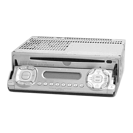
Sony CDX-M770 Service Manual
Fm/am(/lw) compact disc player
Hide thumbs
Also See for CDX-M770:
- Operation instructions manual (254 pages) ,
- Installation/connections (2 pages) ,
- Operating instructions manual (210 pages)
Table of Contents
Advertisement
Quick Links
SERVICE MANUAL
Ver 1.1 2003. 10
• The tuner and CD sections have no adjustments.
SPECIFICATIONS
AUDIO POWER SPECIFICATIONS (US MODEL)
POWER OUTPUT AND TOTAL HARMONIC DISTORTION
23.2 watts per channel minimum continuous average power into
4 ohms, 4 channels driven from 20 Hz to 20 kHz with no more
than 5% total harmonic distortion.
CD player section
Signal-to-noise ratio
90 dB
Frequency response
10 – 20,000 Hz
Wow and flutter
Below measurable limit
Laser Diode Properties (US model)
Material
GaAlAs
Wavelength
780 nm
Emission Duration
Continuous
Laser output power
Less than 44.6 µW*
* This output is the value measured at a distance
of 200 mm from the objective lens surface on the
Optical Pick-up Block.
Tuner section
FM
Tuning range
87.5 – 107.9 MHz (US model)
87.5 – 108.0 MHz (AEP, UK, E model)
Antenna terminal
External antenna connector
Intermediate frequency 10.7 MHz/450 kHz
Usable sensitivity
8 dBf
Selectivity
75 dB at 400 kHz
Signal-to-noise ratio
66 dB (stereo),
72 dB (mono)
Harmonic distortion at 1 kHz
0.6% (stereo),
0.3% (mono)
Separation
35 dB at 1 kHz
Frequency response
30 – 15,000 Hz
AM (US model)
Tuning range
530 – 1,710 kHz
Antenna terminal
External antenna connector
Intermediate frequency 10.7 MHz/450 kHz
Sensitivity
30 µV
Sony Corporation
9-873-504-12
2003J04-1
e Vehicle Company
© 2003. 10
Published by Sony Engineering Corporation
CDX-M770
Model Name Using Similar Mechanism
CD Drive Mechanism Type
Optical Pick-up Name
MW/LW (AEP, UK, E model)
Tuning range
MW: 531 – 1,602 kHz
LW: 153 – 279 kHz
Aerial terminal
External aerial connector
Intermediate frequency 10.7 MHz/450 kHz
Sensitivity
MW: 30 µV
LW: 40 µV
Power amplifier section
Outputs
Speaker outputs (sure seal connectors)
Speaker impedance
4 – 8 ohms
Maximum power output 52 W × 4 (at 4 ohms)
General
Outputs
Audio outputs (front/rear)
Subwoofer output (mono)
Power antenna relay
control lead (US model)
Power aerial relay
control lead (AEP, UK, E model)
Power amplifier control
lead
FM/AM COMPACT DISC PLAYER
FM/MW/LW COMPACT DISC PLAYER
US Model
AEP Model
UK Model
E Model
CDX-M700R/M750
MG-383V-121//K
KSS-720A
– Continued on next page –
US Model
AEP, UK, E Model
1
Advertisement
Table of Contents

Related Manuals for Sony CDX-M770


Summary of Contents for Sony CDX-M770
- Page 1 530 – 1,710 kHz FM/MW/LW COMPACT DISC PLAYER Antenna terminal External antenna connector Intermediate frequency 10.7 MHz/450 kHz Sensitivity 30 µV AEP, UK, E Model Sony Corporation 9-873-504-12 2003J04-1 e Vehicle Company © 2003. 10 Published by Sony Engineering Corporation...
-
Page 2: Service Notes
COMPONENTS IDENTIFIED BY MARK 0 OR DOTTED LINE WITH MARK 0 ON THE SCHEMATIC DIAGRAMS AND IN THE PARTS LIST ARE CRITICAL TO SAFE OPERATION. REPLACE THESE COMPONENTS WITH SONY PARTS WHOSE PART NUMBERS APPEAR AS SHOWN IN THIS MANUAL OR IN SUPPLEMENTS PUBLISHED BY SONY. -
Page 3: Table Of Contents
CDX-M770 NOTE FOR THE OPENING OF THE FRONT PANEL TABLE OF CONTENTS In this set, the front panel is lowered to below the bottom face when it is opened. 1. GENERAL ................4 When servicing the set, place it on a stand having a height of about 2 cm. -
Page 4: General
CDX-M770 SECTION 1 GENERAL This section is extracted from instruction manual. US MODEL AEP, UK, E MODEL... - Page 5 CDX-M770 US, AEP, UK, E MODEL...
- Page 6 CDX-M770 US MODEL...
- Page 7 CDX-M770 AEP, UK, E MODEL...
- Page 8 CDX-M770...
- Page 9 CDX-M770...
- Page 10 CDX-M770 US, AEP, UK, E MODEL...
- Page 11 CDX-M770...
- Page 12 CDX-M770 US MODEL Connection...
- Page 13 CDX-M770...
- Page 14 CDX-M770 AEP, UK, E MODEL Connection...
- Page 15 CDX-M770...
-
Page 16: Disassembly
CDX-M770 SECTION 2 DISASSEMBLY Note : This set can be disassemble according to the following sequence. 2-2. FRONT PANEL ASSY (INOPERATIVE) Front Panel Assy (Normal) CD Mechanism Block, Front Panel (KEY) Assy Front Panel Assy (Inoperative) 4 screw (panel) Sub Panel (CD) Sub Assy... -
Page 17: Sub Panel (Cd) Sub Assy
CDX-M770 2-4. SUB PANEL (CD) SUB ASSY 1 CN603 4 claw 3 PTT 2.6x6 5 claw 2 PTT 2.6 x6 6 sub panel (CD) sub assy 2-5. MOTOR BLOCK ASSY, CAM (R) ASSY Note : Install the motor block assy and cam (R) assy in this roder. -
Page 18: Main Board
CDX-M770 2-6. MAIN BOARD 5 MAIN board 4 PTT 2.6x6 ground point 3 PTT 2.6x6 ground point 2 PTT 2.6x6 1 PTT 2.6x6 2-7. HEAT SINK 5 heat sink 4 PTT 2.6x6 3 PTT 2.6x10 2 PTT 2.6x6 1 PTT 2.6x6... -
Page 19: Chassis (T) Sub Assy
CDX-M770 2-8. CHASSIS (T) SUB ASSY 2 P 2x3 3 P 2x3 1 Unsolder the 4 chassis (T) sub assy lead wires. black white 2-9. LEVER SECTION 5 guide (disc) 6 lever (R) 3 tension spring (LR) 7 lever (L) -
Page 20: Servo Board
CDX-M770 2-10. SERVO BOARD 7 special screws 6 special screws 2 CN2 3 Removal the solders. 1 CN3 4 P 2x3 8 SERVO board 5 loading motor assy 2-11. SHAFT ROLLER ASSY 3 retaing ring (RA) shaft retainer (roller) washer... -
Page 21: Floating Block Assy
CDX-M770 2-12. FLOATING BLOCK ASSY 6 floating block assy 7 compression spring (FL) 1 tension spring (KF1) 8 compression spring (FL) 4 Fit lever (D) in the direction of the arrow. 5 Turn loading ring in the direction of the arrow. -
Page 22: Phase Alignment
CDX-M770 SECTION 3 PHASE ALIGNMENT 3-1. ARM (A-L) ASSY, ARM (B-L) ASSY 3 arm (A-L) assy 4 stop ring 1.5, type-E 2 stop ring 1.5, type-E 1 arm (B-L) assy bracket (L) assy 3-2. CAM (L) 1 Move the arm (B-L) assy in the direction of the arrow A and the arm (A-L) assy in the direction of 3 stop ring 1.5, type-E... -
Page 23: Motor Block
CDX-M770 3-3. MOTOR BLOCK 1 Turn the cam (L) and position the cam so that part A does not touch the SWITCH board SW900. 3 PTT 2.6x6 4 PTT 2.6x6 2 motor block SWITCH board 5 PTT 2.6x6 SW1001 SW1002 cam (L) 3-4. -
Page 24: Arm (A-R) Assy, Arm (B-R) Assy
CDX-M770 3-5. ARM (A-R) ASSY, ARM (B-R) ASSY 4 stop ring 1.5, type-E 3 arm (A-R) assy 2 stop ring 1.5, type-E 1 arm (B-R) assy bracket (R) assy 3-6. CAM (R) 3 stop ring 1.5, type-E 1 Move the arm (B-R) assy in the direction of the arrow A and the arm (A-R) assy in the direction of the arrow B fully (full open state). -
Page 25: Diagrams
CDX-M770 SECTION 4 DIAGRAMS 4-1. IC PIN DESCRIPTIONS • IC501 CXD2598Q (DIGITAL SERVO, DIGITAL SIGNAL PROCESSOR) (SERVO BOARD) Pin No. Pin Name Pin Description DVDD — Digital power supply pin DVSS — Digital ground SOUT Servo brock serial data output (Not used.) SOCK Servo brock serial data read clock output (Not used.) - Page 26 CDX-M770 Pin No. Pin Name Pin Description Tracking error signal input Center servo analog input RFDC RF signal input ADIO Test pin (Not used.) AVSSO — Analog ground IGEN Constant current input from OP amplifier. AVDDO — Analog ground ASYO EFM full-swing output (“L”: VSS, “H”: VDD)
- Page 27 CDX-M770 • IC5 CXP84640-072Q (CD SYSTEM CONTROL) (SERVO BOARD) Pin No. Pin Name Pin Description ITRPT — Not used in this set. 2, 3 — — Not used in this set. 4, 5 — Not used in this set. OPEN...
- Page 28 CDX-M770 Pin No. Pin Name Pin Description SENS SENS signal input — — Not used in this set. — — Not used in this set. BU.IN Back-up power detection input BUSON Bus on control input IN SW Disc in switch input (SW3)
- Page 29 CDX-M770 • IC901 CXD2727Q-4 (DIGITAL SIGNAL PROCESSOR, DIGITAL FILTER, D/A CONVERTER) (MAIN BOARD) Pin No. Pin Name Pin Description DGND — Ground terminal (digital system) 2 – 21 Input terminal for the test (fixed at “L”) 22 – 24 JPE1 – JPE3 External condition jump terminal “H”: condition jump (fixed at “L”)
- Page 30 CDX-M770 Pin No. Pin Name Pin Description DVDD — Power supply terminal (+3.3 V) (digital system) DVSS — Ground terminal (digital system) 67 – 69 SO1 – SO3 Serial data output terminal (Not used.) SOUT Serial data output terminal (Not used.)
- Page 31 BUS ON BUS ON signal BEEP Beep signal TEL ATT Telephone mute signal UNI SI SONY BUS serial data input UNI SO SONY BUS serial data output UNI CKO SONY BUS serial clock output 20 – 23 (NCO) Not used. (Open)
- Page 32 CDX-M770 Pin No. Pin Name Pin Description DDC ON DC/DC converter power control signal CD EJECT OK CD eject control signal CD OPEN REQ Front panel open request signal (NCO) Not used. (Open) OPEN KEY OPEN key detection signal NOSE SW Nose SW detection signal —...
- Page 33 CDX-M770 Pin No. Pin Name Pin Description 4V SEL 4V select control signal (NCO) Not used. (Open) TUN ON Tuner power control signal LED SW1 Illumination select control signal 1 LED SW2 Illumination select control signal 2 (NCO) Not used. (Open) (NCO) Not used.
- Page 34 CDX-M770 • IC702 HD643255A36F (SUB SYSTEM CONTROL) Pin No. Pin Name Pin Description SA CLK Not used. (Open) Not used. (Open) — Ground — Not used. (Open) — Power supply pin (+ 5V) 6 – 9 PC0 – PC3 Not used. (Open) —...
-
Page 35: Circuit Boards Location
Power supply pin (+5 V) SERVO board SWITCH board 90 – 96 PF6 – PF0 Not used. (Open) UNI SO SONY BUS serial data output UNI SI SONY BUS serial data input 99, 100 — Ground UNI CKI SONY BUS serial clock input Not used. -
Page 36: Block Diagram -Cd Section
CDX-M770 4-3. BLOCK DIAGRAM — CD SECTION — TUNER RF AMP, LD APC, DIGITAL SERVO, SECTION DISPLAY OPTICAL PICK-UP CD SYSTEM CONTROL SYSTEM CONTROL ERROR AMP DIGITAL SIGNAL PROCESSOR (Page 37) KSS-720A (Page 38) IC501 (1/3) IC501 SECTION • Signal path... -
Page 37: Block Diagram -Tuner Section
CDX-M770 4-4. BLOCK DIAGRAM — TUNER SECTION — PJ401 –1 BUS AUDIO IN –2 R-CH ELECTRONIC VOLUME IC304 CN303 IC305 –5 R-CH BUSL OUT FL AUDIO OUT Q301 7 AUXL FRONT –6 LINE R-CH 34 ACIFLR 33 AC INLR TUNER UNIT... -
Page 38: Block Diagram -Display Section
CDX-M770 4-5. BLOCK DIAGRAM — DISPLAY SECTION — SUB SYSTEM CONTROL IC702 BUS SI UNI SI SP-SI SP CKI UNI SO UNI SO IC901 SYSTEM CONTROL BUS CLK UNI SCK AD ON IC906 IC501 (3/3) BUS ON BUS ON BU 5V CONT. - Page 39 CDX-M770 • Waveforms • Waveforms THIS NOTE IS COMMON FOR PRINTED WIRING BOARDS AND SCHEMATIC DIAGRAMS. — Servo Board — Main Board — — (In addition to this, the necessary note is (MODE: CD PLAY) (MODE: FM) printed in each block.) for schematic diagram: •...
-
Page 40: Printed Wiring Boards -Cd Mechanism Section
CDX-M770 4-6. PRINTED WIRING BOARDS — CD MECHANISM SECTION —... - Page 41 CDX-M770 • Semiconductor Location Ref. No. Location IC501 Q101 (Page 45)
-
Page 42: Schematic Diagram -Cd Mechanism Section (1/2)
CDX-M770 • Refer to page 39 for Waveforms. 4-7. SCHEMATIC DIAGRAM — CD MECHANISM SECTION (1/2) — • Refer to page 56 for IC Block Diagrams. IC B/D (Page 43) (Page 48) Note: • Voltage is dc with respect to ground under no-signal conditions. -
Page 43: Schematic Diagram -Cd Mechanism Section (2/2)
CDX-M770 • Refer to page 39 for Waveforms. 4-8. SCHEMATIC DIAGRAM — CD MECHANISM SECTION (2/2) — • Refer to page 56 for IC Block Diagrams. (Page 42) IC B/D (Page 42) Note: • Voltage is dc with respect to ground under no-signal conditions. -
Page 44: Printed Wiring Boards -Main Section
CDX-M770 4-9. PRINTED WIRING BOARDS — MAIN SECTION — • Semiconductor Location Ref. No. Location Ref. No. Location D104 IC652 D107 IC702 I-12 IC801 H-11 D109 D202 C-13 IC901 D203 C-13 IC902 D204 G-10 IC904 D205 F-11 IC905 F-10 D301... - Page 45 CDX-M770 AEP,UK model BATT (Page 41) US,Canadian model • Semiconductor Location Ref. No. Location Ref. No. Location Ref. No. Location D101 D602 IC309 D102 D603 IC701 I-12 D103 D607 IC909 D105 D608 D106 D610 Q103 D401 D611 Q106 D501 D612...
-
Page 46: Schematic Diagram -Main Section (1/4)
CDX-M770 • Refer to page 39 for Waveforms. 4-10. SCHEMATIC DIAGRAM — MAIN SECTION (1/4) — • Refer to page 56 for IC Block Diagrams. IC B/D (Page 47) IC B/D (Page 48) Note: • Voltage is dc with respect to ground under no-signal (detuned) condition. -
Page 47: Schematic Diagram -Main Section (2/4)
CDX-M770 4-11. SCHEMATIC DIAGRAM — MAIN SECTION (2/4) — • Refer to page 56 for IC Block Diagrams. IC B/D (Page 46) IC B/D IC B/D (Page 48) Note: • Voltage is dc with respect to ground under no-signal (detuned) condition. -
Page 48: Schematic Diagram -Main Section (3/4)
CDX-M770 • Refer to page 39 for Waveforms. 4-12. SCHEMATIC DIAGRAM — MAIN SECTION (3/4) — • Refer to page 56 for IC Block Diagrams. (Page 46) (Page 47) IC B/D (Page 42) (Page 49) IC B/D Note: • Voltage is dc with respect to ground under no-signal (detuned) condition. -
Page 49: Schematic Diagram -Main Section (4/4)
CDX-M770 • Refer to page 39 for Waveforms. 4-13. SCHEMATIC DIAGRAM — MAIN SECTION (4/4) — • Refer to page 56 for IC Block Diagrams. (Page 53) (Page (Page 51) IC B/D Note: • Voltage is dc with respect to ground under no-signal (detuned) condition. -
Page 50: Printed Wiring Board -Sub (Cd) Section
CDX-M770 4-14. PRINTED WIRING BOARD — SUB (CD) SECTION — (Page 45) • Semiconductor Location Ref. No. Location D901 B-10 D902 D903 D906 B-10 D907 (D908) B-13 IC901 B-13 Q901 Q902 ) : SIDE B... -
Page 51: Schematic Diagram -Sub (Cd) Section
CDX-M770 4-15. SCHEMATIC DIAGRAM — SUB (CD) SECTION — • Refer to page 57 for IC Block Diagram. (Page 49) IC B/D Note: • Voltage is dc with respect to ground under no-signal (detuned) condition. no mark : FM... -
Page 52: Printed Wiring Board -Key Section
CDX-M770 4-16. PRINTED WIRING BOARD — KEY SECTION — • Semiconductor Location Ref. No. Location Ref. No. Location Ref. No. Location (D7) LED5 LED14 A-13 (Page 54) (Page 44) (D8) LED6 LED15 A-11 LED7 LED16 C-11 (IC1) LED8 LED17 B-12... -
Page 53: Schematic Diagram -Key Section
CDX-M770 4-17. SCHEMATIC DIAGRAM — KEY SECTION — (Page 55) (Page Note: • Voltage is dc with respect to ground under no-signal (detuned) condition. no mark : FM... -
Page 54: Printed Wiring Board -Display Section
CDX-M770 4-18. PRINTED WIRING BOARD — DISPLAY SECTION — (Page 52) • Semiconductor Location Ref. No. Location Ref. No. Location Ref. No. Location (D61) A-11 (IC60) LED66 (D62) (IC61) B-11 LED67 B-12 (D63) (IC62) A-13 LED68 (D64) LED69 C-12 (D65) -
Page 55: Schematic Diagram -Display Section
CDX-M770 4-19. SCHEMATIC DIAGRAM — DISPLAY SECTION — • Refer to page 57 for IC Block Diagrams. (Page IC B/D Note: • Voltage is dc with respect to ground under no-signal (detuned) condition. no mark : FM... - Page 56 CDX-M770 • IC BLOCK DIAGRAMS IC1 CXA2596M IC7 LA6576L-TE-L IC306 TC7660SE0A713 8 V+ APC PD AMP 7 OSC HOLD S-GND – 6 LV INPUT 5 VOUT CH2-CH4 OUTPUT – 35 MUTE2 MUTE2 ON/OFF AGCVTH 23 LC/PD BOOST CH1 OUTPUT OSCILLATOR...
- Page 57 CDX-M770 IC305 TDA7402TR 33 32 31 24 23 MIXER MONO- MONO- MONO- MONO- MONO- MONO- FADER FADER FADER FADER FADER FADER ACINLF FRONT SUBWOOFER SWINR ACIN +PHASE OUTPUT SWINL REAR CONTROL SELECTOR ACOUTR MAIN ACOUTL SECOND CREF VOICE BANDPASS BASS...
-
Page 58: Exploded Views
CDX-M770 SECTION 5 EXPLODED VIEWS NOTE: The components identified by • The mechanical parts with no reference • Color Indication of Appearance Parts mark 0 or dotted line with mark number in the exploded views are not supplied. Example : 0 are critical for safety. -
Page 59: Cam Section
CDX-M770 5-2. CAM SECTION M601 Ref. No. Part No. Description Remark Ref. No. Part No. Description Remark 3-230-495-01 CAM (L) * 60 1-681-375-11 SW BOARD X-3380-549-1 ARM (B-R) ASSY * 61 X-3378-711-1 BRACKET (MOTOR) ASSY X-3380-544-1 BRACKET (L) ASSY 3-230-494-01 GEAR (C) -
Page 60: Main Board Section
CDX-M770 5-3. MAIN BOARD SECTION TUX201 F901 Ref. No. Part No. Description Remark Ref. No. Part No. Description Remark X-3380-558-1 CHASSIS (CD) ASSY * 110 3-230-509-01 CHASSIS, BACK * 102 3-230-417-01 SHEET, INSULATING * 111 3-019-565-01 BRACKET (IC) 3-230-493-01 GEAR (DRIVE SHAFT) -
Page 61: Front Panel (Key) Assy Section
CDX-M770 5-4. FRONT PANEL (KEY) ASSY SECTION front panel (DSPL) assy not supplied (KEY board) LCD1 Ref. No. Part No. Description Remark Ref. No. Part No. Description Remark X-3380-535-1 PANEL (KEY) SUB ASSY, FRONT (US) * 164 3-230-486-01 HOLDER (LCD-KEY) -
Page 62: Front Panel (Dspl) Assy Section
CDX-M770 5-5. FRONT PANEL (DSPL) ASSY SECTION LCD60 not supplied (DISPLAY board) Ref. No. Part No. Description Remark Ref. No. Part No. Description Remark 3-230-470-01 PANEL (FRONT BACK) * 209 3-230-466-01 HOLDER (LCD-DSPL) 3-230-472-01 SPRING (LOCK), TENSION 3-230-426-01 BUTTON (OPEN) -
Page 63: Cd Mechanism Section (1)
CDX-M770 5-6. CD MECHANISM SECTION (1) (MG-383V-121//K) M903 Ref. No. Part No. Description Remark Ref. No. Part No. Description Remark * 251 1-676-709-11 IN SELF SW BOARD 3-040-040-01 ARM (ROLLER) 3-040-039-01 CHASSIS (T) * 261 A-3294-808-A SERVO BOARD, COMPLETE 3-040-038-01 SPRING (LR), TENSION... -
Page 64: Cd Mechanism Section (2)
CDX-M770 5-7. CD MECHANISM SECTION (2) (MG-383V-121//K) not supplied Ref. No. Part No. Description Remark Ref. No. Part No. Description Remark 3-040-025-01 ARM, CHUCKING 3-040-033-01 SPRING (KF1), TENSION 3-040-031-01 DAMPER (T) A-3307-422-A CHASSIS (M) COMPLETE ASSY 3-040-056-01 LEVER (D) 3-040-059-01 SPRING (TR), TENSION... -
Page 65: Cd Mechanism Section (3)
CDX-M770 5-8. CD MECHANISM SECTION (3) (MG-383V-121//K) M901 (Supplied with 351) M902 The components identified by mark 0 or dotted line with mark 0 are critical for safety. Replace only with part number specified. Ref. No. Part No. Description Remark Ref. -
Page 66: Electrical Parts List
1-107-826-11 CERAMIC CHIP 0.1uF < DIODE > 1-107-826-11 CERAMIC CHIP 0.1uF 1-107-826-11 CERAMIC CHIP 0.1uF LED60 8-719-079-49 LED LWT673-R1S2-34 (SONY) 1-115-412-11 CERAMIC CHIP 680PF LED62 8-719-076-58 LED NSSW440-BRS (LCD BACK LIGHT) LED63 8-719-076-58 LED NSSW440-BRS (LCD BACK LIGHT) 1-165-176-11 CERAMIC CHIP 0.047uF... - Page 67 CDX-M770 DISPLAY DISC IN SW Ref. No. Part No. Description Remark Ref. No. Part No. Description Remark 1-216-811-11 METAL CHIP 1/16W 1-165-176-11 CERAMIC CHIP 0.047uF 1-216-805-11 METAL CHIP 1/16W 1-165-176-11 CERAMIC CHIP 0.047uF 1-216-864-11 SHORT 1-164-156-11 CERAMIC CHIP 0.1uF 1-216-841-11 METAL CHIP...
- Page 68 CDX-M770 LIMIT SW Ref. No. Part No. Description Remark Ref. No. Part No. Description Remark LSW15 1-771-476-11 SWITCH, KEYBOARD (WITH LED) (TA) 1-216-825-11 METAL CHIP 2.2K 1/16W (AEP,UK,E) 1-216-825-11 METAL CHIP 2.2K 1/16W LSW18 1-771-883-11 SWITCH, TACTILE (WITH LED) (DISC –) 1-216-825-11 METAL CHIP 2.2K...
- Page 69 CDX-M770 MAIN Ref. No. Part No. Description Remark Ref. No. Part No. Description Remark A-3283-163-A MAIN BOARD, COMPLETE (US) C202 1-164-156-11 CERAMIC CHIP 0.1uF A-3283-177-A MAIN BOARD, COMPLETE (AEP,UK,E) C205 1-164-156-11 CERAMIC CHIP 0.1uF C206 1-164-156-11 CERAMIC CHIP 0.1uF *********************...
- Page 70 CDX-M770 MAIN Ref. No. Part No. Description Remark Ref. No. Part No. Description Remark C307 1-162-964-11 CERAMIC CHIP 0.001uF C360 1-126-382-11 ELECT 100uF (AEP,UK,E) C361 1-126-786-11 ELECT 47uF C308 1-162-927-11 CERAMIC CHIP 100PF C362 1-127-573-11 CERAMIC CHIP C309 1-125-837-11 CERAMIC CHIP 6.3V...
- Page 71 CDX-M770 MAIN Ref. No. Part No. Description Remark Ref. No. Part No. Description Remark C515 1-124-584-00 ELECT 100uF C928 1-164-156-11 CERAMIC CHIP 0.1uF C516 1-162-920-11 CERAMIC CHIP 27PF C929 1-164-156-11 CERAMIC CHIP 0.1uF C517 1-164-160-11 CERAMIC CHIP 20PF C930 1-164-156-11 CERAMIC CHIP 0.1uF...
- Page 72 CDX-M770 Ver 1.1 MAIN Ref. No. Part No. Description Remark Ref. No. Part No. Description Remark < DIODE > D652 8-719-820-05 DIODE 1SS181 D801 8-719-977-12 DIODE DTZ6.8B D101 8-719-055-30 DIODE D1FS4A-TA D802 8-719-078-81 DIODE DF5A6.8FU(TE85R) D102 8-719-055-30 DIODE D1FS4A-TA D803...
- Page 73 CDX-M770 MAIN Ref. No. Part No. Description Remark Ref. No. Part No. Description Remark < JACK > Q401 8-729-049-13 TRANSISTOR UPA1853GR-9JG-E1 Q402 8-729-038-68 TRANSISTOR KRC103S J651 1-566-822-41 JACK (REMOTE IN) (AEP,UK,E) Q404 8-729-038-68 TRANSISTOR KRC103S Q405 8-729-120-28 TRANSISTOR 2SC1623-L5L6 < COIL >...
- Page 74 CDX-M770 MAIN Ref. No. Part No. Description Remark Ref. No. Part No. Description Remark R134 1-216-821-11 METAL CHIP 1/16W R309 1-216-839-11 METAL CHIP 1/16W R135 1-216-057-00 METAL CHIP 2.2K 1/10W R310 1-216-841-11 METAL CHIP 1/16W R136 1-216-057-00 METAL CHIP 2.2K...
- Page 75 CDX-M770 MAIN Ref. No. Part No. Description Remark Ref. No. Part No. Description Remark R377 1-216-864-11 SHORT R512 1-216-815-11 METAL CHIP 1/16W R379 1-216-805-11 METAL CHIP 1/16W R513 1-216-821-11 METAL CHIP 1/16W R380 1-216-841-11 METAL CHIP 1/16W R514 1-216-841-11 METAL CHIP...
- Page 76 CDX-M770 MAIN Ref. No. Part No. Description Remark Ref. No. Part No. Description Remark R606 1-216-809-11 METAL CHIP 1/16W R815 1-216-845-11 METAL CHIP 100K 1/16W (AEP,UK,E) R816 1-216-809-11 METAL CHIP 1/16W R607 1-216-809-11 METAL CHIP 1/16W R817 1-216-821-11 METAL CHIP...
- Page 77 CDX-M770 SERVO MAIN Ref. No. Part No. Description Remark Ref. No. Part No. Description Remark R947 1-216-831-11 METAL CHIP 6.8K 1/16W C117 1-164-733-11 CERAMIC CHIP 820PF R948 1-216-833-11 METAL CHIP 1/16W C118 1-164-360-11 CERAMIC CHIP 0.1uF R949 1-216-833-11 METAL CHIP...
- Page 78 CDX-M770 SERVO SUB (CD) Ref. No. Part No. Description Remark Ref. No. Part No. Description Remark < TRANSISTOR > R515 1-216-864-11 SHORT R516 1-216-845-11 METAL CHIP 100K 1/16W Q101 8-729-904-87 TRANSISTOR 2SB1197K-T-146-R R517 1-216-837-11 METAL CHIP 1/16W R524 1-216-845-11 METAL CHIP...
- Page 79 CDX-M770 SUB (CD) Ref. No. Part No. Description Remark Ref. No. Part No. Description Remark D906 8-719-422-41 DIODE MA8051-L-TX ACCESSORIES & PACKING MATERIALS D907 8-719-977-12 DIODE MA8068-M-TX ******************************** D908 8-719-083-14 DIODE RRX9000-0501 1-476-546-11 REMOTE COMMANDER (RM-X111) (AEP,UK,E) < FERRITE BEAD >...
- Page 80 CDX-M770 Ref. No. Part No. Description Remark PARTS FOR INSTALLATION AND CONNCTIONS ************************************** 3-014-370-21 FRAME, FITTING 3-916-012-01 BRACKET (ND), FITTING ASSIST (US) 7-682-160-01 SCREW +P 4X6 (US) X-3368-725-1 SCREW ASSY, FITTING (US) 3-386-828-01 SCREW, FITTING (AEP,UK,E) 3-349-410-01 BUSHING (AEP,UK,E) X-3366-405-1 SCREW ASSY (EXP), FITTING (AEP,UK,E)
- Page 81 CDX-M770 MEMO...
- Page 82 CDX-M770 REVISION HISTORY Clicking the version allows you to jump to the revised page. Also, clicking the version at the upper on the revised page allows you to jump to the next revised page. Ver. Date Description of Revision 2001. 03 2003.
Need help?
Do you have a question about the CDX-M770 and is the answer not in the manual?
Questions and answers