Table of Contents
Advertisement
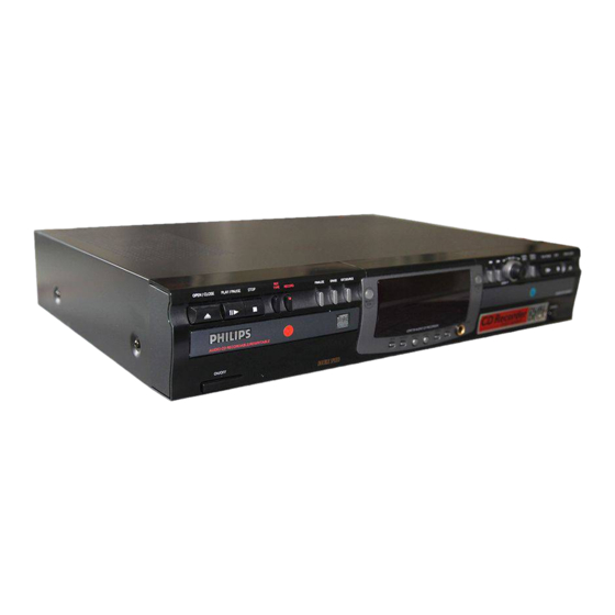
Compact disc recorder
SERVICING
For servicing CDR779, the set can be devided into three parts
1. The display board (partly) 1002, the I/O board 1004, the
headphone board (partly) 1002, the IR board (partly) 1002, the
ON/OFF & Standby LED board (partly) 1002 and the CD-out
board (partly) 1002 have to be repaired at component level. The
power supply unit 1003 is available as spare part, but can also be
repaired at component level.
2. The CDR module (containing the CDR loader 81, CDR main
board 1001 and loader bracket 82, 83) can also be repaired at
component level with the help of COMPAIR release 1.6 and
higher. With this tool the diagnosing of the set can be done in an
interactive way. In the tool also the adjustment procedure has
been implemented. This is absolutely necessary in case the CDR
mainboard and/or (CDR loader) CDM is disconnected from the
matched production combination. Only designated workshops
can perform these repairs. Please send the complete set to the
designated workshop.
3. The CD module (containing the CD loader 131, CD mainboard
1005 and loader bracket 132) is a new module with VAL1250
loader assy but also a separate CDM and separate loader parts
will be available via service stock. The CD mainboard can be
repaired at component level.
Also available : Circuit Description "The Basics of Compact Disc
Recordable/Rewriteable". Service codenumber 4822 725 25242.
Second line Repairmanual . Service codenumber 3104 125 40110.
©
Copyright 2000 Philips Consumer Electronics B.V. Eindhoven, The Netherlands.
All rights reserved. No part of this publication may be reproduced, stored in a
retrieval system or transmitted, in any form or by any means, electronic, mechanical,
photocopying, or otherwise without the prior permission of Philips.
Published by DP 0071 Service DPS Hasselt
OPEN / CLOSE
OPEN / CLOSE
OPEN / CLOSE
PLAY / PAUSE
PLAY / PAUSE
PLAY / PAUSE
STOP
STOP
STOP
AUDIO CD RECORDAB LE/REWRITA BLE
AUDIO CD RECORDAB LE/REWRITA BLE
AUDIO CD RECORDAB LE/REWRITA BLE
ON / OFF
Printed in the Netherlands
REC
RECORD
EXT
EXT
TYPE
FINALIZE
FINALIZE
ERASE
ERASE
SOURCE
SOURCE
Recordable
CDR775 AUDIO CD RECORDER
PROG
SHUFFLE
PHONES
DISPLAY
SCROLL
REPEAT
DJ MODE
Contents
Subject to modification
/00
EASY JOG
EASY JOG
STORE/
STORE/
CANCEL/
CANCEL/
5
5
6
6
J
J
K
K
MENU
MENU
DELETE
DELETE
PLAY/PAUSE
PLAY/PAUSE
STOP
STOP
OPEN/CLOSE
OPEN/CLOSE
ENTER
AUDIO CD PLAYBACK
AUDIO CD PLAYBACK
IR SENSOR
CL 96532086_000.eps
080999
Page
2
4
7
19
20
21
22
23
Diagram PWB
24
25
26
27
27
28
28
29
35
(Diagram 2)
30
35
(Diagram 3)
31
35
(Diagram 4)
32
35
33
35
34
35
36
37
42/43
(Diagram 1B) 39
42/43
(Diagram 1C) 40
42/43
41
42/43
45
49
55
69
75
5 3104 125 40190
Advertisement
Table of Contents

Subscribe to Our Youtube Channel
Related Manuals for Philips CDR779


Summary of Contents for Philips CDR779
-
Page 1: Table Of Contents
Contents Page 1. Technical Specifications 2. Warning and Servicing Hints For servicing CDR779, the set can be devided into three parts 3. User Instructions 4. Mechanical Instructions 1. The display board (partly) 1002, the I/O board 1004, the Wiring Diagram CDR... -
Page 2: Cdr779 /00
GB 2 CDR779 Technical Specifications CDR779 1. Technical Specifications CDR779 General : typical: 98dB. Dynamic range : > 94dB. at 1kHz. : typical: 95dB. Mains voltage : all range version 84- THD+N : > 89dB from 20Hz. 230V until 20kHz. - Page 3 Technical Specifications CDR779 CDR779 GB 3 1.3.4 Headphone output (all functions) Output voltage : 2Vrms (0dB)/16Ω : > 80dB THD+N : > 78dB Channel separation : > 60dB between 20Hz until 20kHz Laser device Material : GaAlAs Wave length : between 780 and 800nm (at 25°C)
-
Page 4: Warning And Servicing Hints
GB 4 CDR779 Warnings and Servicing Hints 2. Warnings and Servicing Hints WARNING WAARSCHUWING All ICs and many other semi-conductors are Alle IC's en vele andere halfgeleiders zijn susceptible to electrostatic discharges (ESD). gevoelig voor elektrostatische ontladingen Careless handling during repair can reduce (ESD). - Page 5 Warnings and Servicing Hints CDR779 GB 5 SERVICING HINTS In the set, chip components have been applied. For disassembly and assembly check the figure below. CL 96532086_022.eps 080999...
- Page 6 GB 6 CDR779 Warnings and Servicing Hints CL 96532086_023.eps 080999...
-
Page 7: User Instructions
Directions for use CDR779 GB 7 3. Directions for use English... - Page 8 GB 8 CDR779 Directions for use English...
- Page 9 Directions for use CDR779 GB 9 English...
- Page 10 GB 10 CDR779 Directions for use English...
- Page 11 Directions for use CDR779 GB 11 English...
- Page 12 GB 12 CDR779 Directions for use English...
- Page 13 Directions for use CDR779 GB 13 English...
- Page 14 GB 14 CDR779 Directions for use English...
- Page 15 Directions for use CDR779 GB 15 English...
- Page 16 GB 16 CDR779 Directions for use English...
- Page 17 Directions for use CDR779 GB 17 English...
- Page 18 GB 18 CDR779 Directions for use English...
-
Page 19: Mechanical Instructions
Mechanical instructions CDR779 GB 19 4. Mechanical instructions Wiring diagram WIRING DIAGRAM CDR779 8006 Pin 1 indicated by All Wires are 1/1. 3104 157 1099 8003 8001 8002 POWER SUPPLY UNIT VDC2 GROUND VDC2 VFTD +12V VFTD 3122 427 21573... -
Page 20: Wiring Diagram Cd Loader
Mechanical instructions CDR779 GB 20 Wiring CD WIRING DIAGRAM CD LOADER VAL1250 CONNECTOR 1006 CONNECTOR 1002 Connection tray motor and tray switch HALL + HOMESW SGND TRAY+ TRAY- HALL- LOADER VAL1250 CONNECTOR 1001 Tray 1002 HOMESW switch UCOIL SGND 1208... -
Page 21: Exploded View Cdr
Mechanical instructions CDR779 GB 21 Exploded view CDR779 EXPLODED VIEW CDR779 LOADER ASSY CD LOADER ASSY CDR MAIN BOARD CDR CD OUT BOARD MAIN BOARD I/O BOARD POWER SUPPLY UNIT ON/OFF & STBY LED DISPLAY BOARD HEADPHONE BOARD BOARD CL 06532151_015.eps... -
Page 22: Exploded View Cd Loader
Mechanical instructions CDR779 GB 22 Exploded view CD EXPLODED VIEW CD LOADER VAL1250 CLAMPER ASSY SUSPENSION CDM VAM1250 RACK SPRING MOTORSPRING SCREW SCREW SUSPENSION RACK SUB CHASSIS RUBBER RUBBER SWITCH SUSPENSION RUBBER PLUG SUSPENSION TRAY GEARWHEEL RUBBER PLUG TULE CHASSIS ASSY VAL1250... -
Page 23: Dismantling Instructions
Mechanical instructions CDR779 GB 23 Dismantling 779 DISMANTLING INSTRUCTIONS CDR779 See exploded views for item numbers Cover 165 assembling ↑ ⇒ → 172, Remove 7 screws 166 2 at each side and 3 at rear side. ↓ ⇒ disassembling Lift cover at rear side to remove. -
Page 24: Block Diagram, Circuit Diagrams And Pwb's
Block diagrams, Circuit diagrams and PWB’s CDR779 GB 24 5. Block diagrams, Circuit diagrams and PWB’s Blockdiagram 779 OVERALL BLOCK DIAGRAM CDR779 CDR MAIN BOARD CDL 4009 DISPLAY ASSY LOADER ASSY 7703 1113 HEADPHONE 7330 CDM3800 DISPLAY 1121 1330 FLASH... -
Page 25: Display Board
Block diagrams, Circuit diagrams and PWB’s CDR779 GB 25 Display 779 0100 G10 F147 E3 1050 H7 F148 E7 1101 B9 F149 F3 1102 C12 F150 F7 DISPLAY BOARD - CIRCUIT DIAGRAM 1103 C11 F151 F7 1104 C12 F152 F3... -
Page 26: Display Board 25
Block diagrams, Circuit diagrams and PWB’s CDR779 GB 26 Display 779 DISPLAY BOARD - BOTTOM VIEW DISPLAY BOARD - TOP VIEW CL 06532151_003.eps 241100... -
Page 27: Ir / On/Off &Standby Led Board 27
F202 IR BOARD - BACK VIEW TO DISPLAY BOARD GNDB PB DISPLAY - 4230 3104 123 4230 ON/OFF & STBY LED BOARD CDR779 - CIRCUIT DIAGRAM 1300 A3 1301 C3 1302 B1 6300 A1 F300 A2 F301 A2 ON/OFF & STBY LED BOARD - FRONT VIEW... -
Page 28: Headphone / Cd-Out Board 28
F112 3107 F113 3104 2105 7104 BC818 F114 3105 3109 F115 CDR779 HP 3104 123 4270.2 CD OUT BOARD - CIRCUIT DIAGRAM CD OUT BOARD - TOP VIEW 1500 A4 3504 D2 1501 C4 5500 A2 5500 7CHA 1502 A1... -
Page 29: I/O Board: Ext Dac (Diagram 1)
Block diagrams, Circuit diagrams and PWB’s CDR779 GB 29 I/O board: Ext DAC 1,4112MHz 44,1KHz LEFT CHANNEL RIGHT CHANNEL 0.5uS/DIV 1100 F14 7103-B E3 1101 G14 7104 B12 2100 A9 7105-A I3 2100 2101 A7 7105-B G3 2102 A3 7107 D8... -
Page 30: I/O Board: Cinch
Block diagrams, Circuit diagrams and PWB’s CDR779 GB 30 I/O board: Cinch 1200-A A12 I237 H11 1200-B B2 I238 I11 1201-A B12 I239 I4 1201-B D1 +5Vd 1201-C C1 3200 I201 1205-A F3 +5Vd 1205-B F12 7200 1200-A 1207 G12... -
Page 31: I/O Board: Mic Adc
Block diagrams, Circuit diagrams and PWB’s CDR779 GB 31 I/O board: Mic ADC 1300 B13 2300 C12 2301 B6 2302 B6 +3V3d 2304 B3 2305 B6 2306 B6 2307 B3 3300 2308 C2 I300 2309 C7 I301 MIC ADC +3V3a... -
Page 32: I/O Board: Power Supply
Block diagrams, Circuit diagrams and PWB’s CDR779 GB 32 I/O board: Power supply 1400 A1 1401 B1 2400 A6 2401 A6 POWER SUPPLY 3400 2402 A7 2403 A8 1400 EH-B I404 7400 2404 B6 L78M09 2405 B6 I400 2406 C6... -
Page 33: I/O Board: Dac Filter (Diagram 5)
Block diagrams, Circuit diagrams and PWB’s CDR779 GB 33 I/O board: DAC filter 2500 A4 7518 H4 2501 A10 7519 I8 2502 A10 7520 A7 2503 B8 7521 D7 I500 I501 3500 2504 C12 7522 F7 +9Va 2506 C8 7523 I7... -
Page 34: I/O Board: Dac (Diagram 6)
Block diagrams, Circuit diagrams and PWB’s CDR779 GB 34 I/O board: DAC 2600 C4 2601 C4 2602 D10 2603 D9 2604 E9 2605 E12 2606 E10 2607 F6 2608 F6 2609 F5 2610 F6 2611 C5 2612 C5 2613 G10... - Page 35 Block diagrams, Circuit diagrams and PWB’s CDR779 GB 35 Layout I/O board I/O BOARD LAYOUT.3 - BOTTOM VIEW I/O BOARD LAYOUT.3 - TOP VIEW CL 06532151_012.eps 241100...
- Page 36 Block diagrams, Circuit diagrams and PWB’s CDR779 GB 36 PSU CDR3-ECU 0101 A2 5225 D9 0125 B5 5226 E9 0205 A12 5230 B10 0206 G7 5240 C9 POWER SUPPLY UNIT CDR3-ECO 0207 A11 5250 C11 3124 0260 2128 0208 A10...
-
Page 37: Power Supply Unit 36
Block diagrams, Circuit diagrams and PWB’s CDR779 GB 37 Layout PSU CDR3-ECO POWER SUPPLY UNIT CDR3-ECO - TOP VIEW POWER SUPPLY UNIT CDR3-ECO - BOTTOM VIEW CL 06532151_014.eps 241100... -
Page 38: Cd-Mainboard: Decoder & Servo (Diagram 1A)
Block diagrams, Circuit diagrams and PWB’s CDR779 GB 38 CD main board: Decoder & servo processor part 1000-1 C1 1000-7 H1 1020 G10 2148 C1 2159 D1 2169 F8 2183 F3 2232 H13 3164 B15 3178 C8 3187 D2 3196 E6... -
Page 39: Cd-Mainboard: Servo Drivers
Block diagrams, Circuit diagrams and PWB’s CDR779 GB 39 CD main board: Servo drivers part 1000-13 E1 F100 F3 1000-14 E1 F101 F1 1000-15 D1 F102 A11 1000-16 D1 F103 A2 CD MAIN BOARD - CIRCUIT DIAGRAM 1B 1001 B1... -
Page 40: Cd-Mainboard: Audio (Diagram 1C)
Block diagrams, Circuit diagrams and PWB’s CDR779 GB 40 CD main board: Audio part 1208-10 C11 F325 G10 1208-11 C11 F329 G10 1208-12 D11 F350 G7 1208-13 D11 F351 G7 CONN. 1208 : TO CDR MAIN BOARD CD MAIN BOARD - CIRCUIT DIAGRAM 1C... - Page 41 Block diagrams, Circuit diagrams and PWB’s CDR779 GB 41 CD main board: Microprocessor part 1205 F7 1206 D12 1207 E12 VPROC VPROC VPROC 3999 CD MAIN BOARD - CIRCUIT DIAGRAM 2 1208-1 E13 1208-15 E13 VPROC VPROC VPROC VPROC 1208-16 D13...
-
Page 42: Cd-Mainboard: Microprocessor (Diagram 2)
Block diagrams, Circuit diagrams and PWB’s CDR779 GB 42 Layout CD Main board (top view) CD MAIN BOARD - TOP VIEW CL 96532086_019.eps 080999... - Page 43 Block diagrams, Circuit diagrams and PWB’s CDR779 GB 43 Layout CD Main board (bottom view) CD MAIN BOARD - BOTTOM VIEW CL 96532086_020.eps 080999...
- Page 44 Block diagrams, Circuit diagrams and PWB’s CDR779 GB 44 Personal notes: Personal notes:...
-
Page 45: Diagnostic Software
Diagnostic Software CDR779 GB 45 6. Diagnostic Software Dealer mode The purpose of the dealer mode is to prevent people taking out the CD inside the player at exhibitions, showrooms etc.. This mode disables the open/close function of the player. - Page 46 GB 46 CDR779 Diagnostic Software Electrical service diagnostics ELECTRICAL SERVICE DIAGNOSTICS (software versions, test for defective components) If power ON, switch power OFF Load CD-DA disc (SBC444A) Press <PLAY> + <F FWD> simultaneously and switch ON unit PLAYER LOADER TESTS...
- Page 47 Switching off the unit processor (DASP) and the CD loader is tested. The test is ends the test. In case of a CDR779, one can check the CD only applicable for CDR779. loader mechanics in the same way by pressing the above key combination on the CD player keys.
- Page 48 GB 48 CDR779 Diagnostic Software 6.4.3 Description of the tests Burn in mode Focus control test 6.6.1 Description: The focussing lens is continuously moving up and down. The display reads "BUSY". The Burn In mode is an endless cycle of: •...
-
Page 49: Faultfinding Trees
Faultfinding trees CDR779 GB 49 7. Faultfinding trees CDR-Module NO DISC LOADED SWITCH ON POWER STBY LED? PRESS <DISPLAY> CHECK: • MAINS, MAINS CABLE • POWER SUPPLY (SEE FAULT FINDING GUIDE PSU) ⇒ WIRING ⇒ ON/OFF SWITCH ⇒ FUSES ⇒... - Page 50 GB 50 CDR779 Faultfinding trees CD-DA DISC LOADED CHECK: • WIRING • POWER SUPPLY VOLTAGES DISC • ELECTRICAL SERVICE DIAGNOSTICS: DETECTION & READING? REPLACE CDR MODULE IF "DERRn" OR "BERRn" ERROR OCCURS CHECK: • DISC: DIRT, SCRATCHES, DAMAGED... DISPLAY: •...
- Page 51 Faultfinding trees CDR779 GB 51 CD-R DISC LOADED CHECK: • DISC WIRING DETECTION & • POWER SUPPLY VOLTAGES READING? • ELECTRICAL SERVICE DIAGNOSTICS: REPLACE CDR MODULE IF "DERRn" OR "BERRn" ERROR OCCURS CHECK: DISPLAY: DISPLAY: • DISC: DIRT, SCRATCHES, DAMAGED...
- Page 52 GB 52 CDR779 Faultfinding trees CD-RW DISC LOADED CHECK: • DISC WIRING DETECTION & • POWER SUPPLY VOLTAGES READING? • ELECTRICAL SERVICE DIAGNOSTICS: REPLACE CDR MODULE IF "DERRn" OR "BERRn" ERROR OCCURS CHECK: DISPLAY: DISPLAY: • DISC: DIRT, SCRATCHES, DAMAGED...
- Page 53 Faultfinding trees CDR779 GB 53 CD Module CD MODULE NO DISC • POWER ON CHECK FLEX CONNECTION FROM CDR MAIN BOARD • POWER SUPPLY ⇒ +5V, +12V AT TESTPOINTS 28 AND 27 ⇒ +5V AT CONN. 1000 PINS 1 AND 3 ⇒...
- Page 54 GB 54 CDR779 Faultfinding trees CD MODULE PLAYBACK PRESS <PLAY> • DAC 7309 TESTPOINTS 20, 21, 22 : I 2 S AT INPUT OF DAC 7309 ⇒ ⇒ CHECK POWER SUPPLY PINS 4, 13 ⇒ CHECK CLK11 AT PIN 6 : 11.2896MHz AUDIO? ⇒...
-
Page 55: Faultfinding Guide
Faultfinding Guide CDR779 GB 55 8. Faultfinding Guide Display Board Display controller TMP87C874F TMP87C874F (IC7104) is a high speed and high performance 8-bit single chip microprocessor, containing 8- 8.1.1 Description of display board bit A/D conversion inputs and a VFT (Vacuum Fluorescent Tube) driver. - Page 56 GB 56 CDR779 Faultfinding Guide 8.1.2 Test instructions line : T7203 for G13, T7204 for G14 and T7100 for G15. A typical grid line signal shows in the oscillogram below. Supply voltages The display board receives several voltages via connector PM3392A 1119 (and connector 1121 for CDR570/930).
- Page 57 In the CDR570/930 the IR receiver TSOP1736 (6101) is mounted on the display board. In the CDR770 that same IR receiver (6200) is mounted on a small board together with the headphone socket. In the CDR779 the IR receiver (6200) is CH1!2.00 V= MTB5.00ms ch1+ mounted on its own small board.
- Page 58 GB 58 CDR779 Faultfinding Guide 8.1.3 Display board troubleshooting guide SWITCH POWER ON, EXIT STAND BY MODE CHECK : • SUPPLY VOLTAGES ⇒ -38V ±5% at conn. 1119-2 ⇒ 3V8 ± 10% between conn. 1119-1 and 1119-3 DISPLAY? ⇒ +5V ± 5 % at conn. 1119-10 (1121-4 for CDR570/930) •...
-
Page 59: Power Supply
Faultfinding Guide CDR779 GB 59 Circuit description of the current mode power supply 8.2.1 Blockdiagram Rectifier 6210 Lightning 5131 Protection MAINS FILTER 2643 6230 +12V Start Overvoltage Circuit Protection Comp 6240 2.5V CLOCK Error 6250 Amplifier 7125 comparator VFTD Verror... - Page 60 GB 60 CDR779 Faultfinding Guide capacitor at the Vcc pin will discharge because the primairy becomes reversed. This results in a current flow through the auxiliary voltage, coming from winding7-9 is below the Vcc tranformer’s secondary winding via the diodes, electrolytic voltage.
- Page 61 Faultfinding Guide CDR779 GB 61 8.2.6 Oscillograms 8.2.7 Circuit description Input circuit Oscillograms The input circuit consists of a lightning protection circuit and an EMI filter. The lightning protection comprises R3120, gasarrestor 1125 and R3124. CH1 2 The EMI filter is formed by C2120, L5120, C2125 and R3124.
- Page 62 GB 62 CDR779 Faultfinding Guide When the regulation circuit is interrupted due to an error in Secondary rectifier/smoothing circuit the control loop, the regulated output voltage will increase There are 5 rectifier/smoothing circuits on the secondary (overvoltage). This overvoltage is sensed on the primary side.
- Page 63 To avoid locking These signals are necessary inputs for the decoder CD10. problems between the two drives in the CDR779, both drives Based on these signals the decoder will control the disc. The run on the same clock.
- Page 64 GB 64 CDR779 Faultfinding Guide Block Diagram 8.3.4 TDA7073A Power Drivers (7021, 7022) SSA2 DDA2 SSD2 Description D1 D2 D3 D4 SSA1 DDA1 SSD1 SSD3 DDD1(P) DDD2(C) The TDA7073A is a dual power driver circuit for servo systems with a single supply. In this configuration it is used to drive the sledge, tray, focus and radial.
- Page 65 Faultfinding Guide CDR779 GB 65 is applied, the square wave on pin 17 will go ahead of the All signals will have a value as shown in the truth table. square wave on pin 18. Check the following output signals :...
- Page 66 GB 66 CDR779 Faultfinding Guide 8.3.7 HF Path then follow another amplification and filtering circuit. The filtering again is controlled by the S1 and S2 lines, dependant on whether the disc starts up (speed n=1, S1 and S2 Low), Description...
- Page 67 Attenuation of - 12dB is not used because this is also done in the decoder. Timing of the I2S-bus, in case of Philips I2S is shown in the next figure :...
- Page 68 GB 68 CDR779 Faultfinding Guide Measurements 1200 - 17 AMPLIFIER CLK11 1200 - 19 NMUTE CL96532086_062.eps 080999 Figure 8-31 Keep processor 7202 in reset by forcing pin 7 of connector 1208 to +5V. This puts the processor outputs in tristate.
-
Page 69: List Of Abbreviations
List of Abbreviations CDR779 GB 69 9. List of Abbreviations SIGNAL NAME SIGNAL FLOW FUNCTION AND DESCRIPTION +12V main supply voltage from PSU +12V supply voltage from PSU +12VA supply voltage +12V supply voltage for Audio part main supply voltage from PSU... - Page 70 IC7270 -> R3324 power save at stop, active low DOBM_CD CONN1708, C2731 -> R3757 -> R3903 - Digital Output (EBU output) from CD player in CDR779 to DASP > IC7701 DOBM_CDR IC7300 -> R3382D -> C2379, IC7701 Digital Output (EBU output) from CDR60 to DASP DRAM_RW IC7701 ->...
- Page 71 R3248A <-> IC7270,R3247D I2C DAta line I2S_BCLK_AI IC7701 -> R3814 -> IC7406 I2S4 Bit CLocK for CODEC (ADC for CDR779) Analog Input (record from analog source) I2S_BCLK_AO IC7701 -> R3894A -> IC7406 I2S2 Bit CLocK for CODEC (DAC for CDR779) Analog Output I2S_BCLK_CD CONN1708, C2739 ->...
- Page 72 +12V supply voltage for servo/Laser part L3_CLK IC7701 -> R3725 -> IC7406 L3 interface CLocK line / control CODEC (not for CDR779) L3_DATA IC7701 <-> R3728 <-> IC7406 L3 interface DATA line with CODEC (not for CDR779) L3_MODE IC7701 ->...
- Page 73 IC7706A -> R3826 -> IC7270 SYstem CLocK Basic Engine (8.4672 MHz) SYS_RESET IC7701 -> R3758 -> CONNF934IC7701 - SYStem RESET to display assy (and CD player for CDR779) > R3770 -> T7707 -> CONN1708 CONN1819 -> R3906, IC7701 JTAG ClocK signal TDSO IC7701 ->...
- Page 74 GB 74 CDR779 List of Abbreviations TXD_TOOL IC7701 -> CONN1818 Transmit of UART for test TOOL U+, U-, V+, V-, CONN1330 -> IC7330 hall feedback signals from turn table motor to hall motor driver W+, W- UCOIL, VCOIL, IC7330 -> CONN1330...
-
Page 75: Partslist (Mechanical And Electrical)
EURO 20PS202 2218 5322 122 32659 33pF 5% 50V 3105 4822 051 20008 0Ω jumper . (0805) 1004 3104 128 06610 PB ASSY 4249 I/O CDR779 2219 5322 122 32659 33pF 5% 50V 3106 4822 051 20472 4k7 5% 0.1W 8005... - Page 76 GB 76 CDR779 Spare parts list 3154 4822 051 20471 470Ω 5% 0.1W 4xxx 4822 051 20008 0Ω 5% 0.25W (0805) 2401 5322 122 31647 1nF 10% 63V 3155 4822 051 20471 470Ω 5% 0.1W 3156 2322 750 64709 RST SM FUSE 1206 47Ω...
- Page 77 Spare parts list CDR779 GB 77 3119 2322 595 90023 VDR DC 1M A/423V S MAX Headphone board 800V B CD MAINBOARD 3123 4822 050 21803 18k 1% 0.6W 3124 4822 117 12181 470Ω 20% 0.5W Miscellaneous 3125 4822 117 10833 10k 1% 0.1W 3126 4822 116 80176 1Ω...
- Page 78 GB 78 CDR779 Spare parts list 2178 4822 126 14585 100nF 10% 50V 3168 4822 117 11373 100Ω 1% RC12H 0805 3313 4822 117 10833 10k 1% 0.1W 2180 4822 124 41796 22µF 20% 16V 3169 4822 051 30272 2k7 5% 0.062W 3314 4822 117 10833 10k 1% 0.1W...
Need help?
Do you have a question about the CDR779 and is the answer not in the manual?
Questions and answers