Table of Contents
Advertisement
Quick Links
SERVICE MANUAL
Picture tube
0.25-0.27 mm aperture grill pitch
19 inches measured diagonally
90-degree deflection
Video image area
(18" maximum viewing image)
Approx. 365 X 274 mm (w/h)
3/8
(14
x 10
Resolution
Horizontal: Max. 1600 dots
Vertical: Max. 1200 lines
Standard image area
Approx. 352 x 264 mm (w/h)
7/8
(13
x 10
Input signal
Video
Analog RGB (75 ohms typical)
0.7 Vp-p, Positive
Sync
External HD/VD, Composite
Polarity Free TTL
Video Composite (Sync on Green)
0.3 Vp-p, Negative
SPECIFICATIONS
7/8
inches)
1/2
inches)
Design and specifications are subject to change without notice.
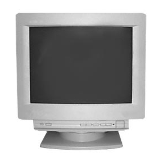
CPD-4201M
Canadian Model
D98
Power Consumption
Maximum
Nominal
Deflection frequency
AC input voltage / current
Dimensions
Mass
COLOR MONITOR
CPD-4201M
US Model
Chassis No. SCC-L20B-A
CHASSIS
130 W
100 W
Horizontal: 30 to 96 KHz
Vertical: 48 to120 Hz
100 to 120 V, 50/60 Hz, 1.7A
220 to 240V, 50/60Hz, 1.2A
444 x 467 x 455 (w/h/d)
(17
1/2
x 18
1/2
x 18 inches)
Approx. 26 kg (57 lb 5 oz)
Advertisement
Table of Contents

Related Manuals for Sony CPD-4201M


Summary of Contents for Sony CPD-4201M
-
Page 1: Service Manual
CPD-4201M SERVICE MANUAL CPD-4201M US Model Canadian Model Chassis No. SCC-L20B-A CHASSIS SPECIFICATIONS Picture tube 0.25-0.27 mm aperture grill pitch Power Consumption 19 inches measured diagonally Maximum 130 W 90-degree deflection Nominal 100 W Video image area (18" maximum viewing image) - Page 2 CPD-4201M POWER SAVING FUNCTION NOTE: If no video signal is input to the monitor, the This monitor has three Power Saving modes. "NO INPUT SIGNAL" message appears. After about By sensing the absence of a video signal from the 30 seconds, the Power Saving function automatically...
- Page 3 CRITIQUE POUR SECURITE FONCTIONNEMENT. NE LES REMPLACER QUE PAR DES COMPOSANTS SONY DONT LE NUMERO DE PIECE EST Earth Ground INDIQUE DANS LE PRESENT MANUEL OU DANS DES SUPPLEMENTS PUBLIES PAR SONY. LES REGLAGES DE CIRCUIT DONT L'IMPORTANCE EST CRITIQUE POUR LA...
-
Page 4: Table Of Contents
CPD-4201M TABLE OF CONTENTS Section Title Page 1. GENERAL .................... 5 2. DISASSEMBLY 2-1. Cabinet Removal ..............11 2-2. Service Position ..............11 2-3. D, A, H and N Board Removal .......... 11 2-4. Picture Tube Removal ............12 3. SAFETY RELATED ADJUSTMENT ........ -
Page 5: General
SECTION 1 The instructions given here are partial abstracts from the Operating Instruction Manual. The page numbers shown reflect those of the Operating Instruction Manual. GENERAL Getting Started Getting Started Setup Table of Contents Connect the monitor to your computer system. Precautions . - Page 6 Getting Started Customizing Your Monitor Customizing Your Monitor The OSD (On-screen Display) System Use of the Tilt/Swivel Adjusting the Picture Brightness and Contrast This monitor can be adjusted within the angles shown below. To 3 If necessary, use the BRIGHTNESS buttons to select a specific turn the monitor vertically or horizontally, hold it at the bottom with Introducing the OSD System item.
- Page 7 Customizing Your Monitor Customizing Your Monitor 3 Adjusting the shape of the 5 Adjusting the color of the picture 6 Adjusting the quality of the Adjusting the Settings picture (GEOM) (COLOR) picture (CONV) 1 Adjusting the centering of the The COLOR settings allow you to adjust the picture’s color The CONV settings allow you to adjust the quality of the picture by The GEOMETRY settings allow you to adjust the rotation and picture (CENTER)
- Page 8 Customizing Your Monitor Customizing Your Monitor 9 Using the GRAPHIC Resetting the adjustments Degaussing the monitor Note • Before using this feature, the monitor must be in normal operation mode The monitor is automatically degaussed (demagnetized) when the ENHANCEMENT OSD (Green power indicator) for at least 30 minutes.
- Page 9 Technical Features Additional Information Specifications Power Saving Function and Warning Messages LED Indicators Picture tube 0.25 – 0.27 mm aperture grill pitch, If there is something wrong with the input signal, one of the following messages appears. 19 inches measured diagonally, 1 Out of Scan Range INFORMATION This monitor has three Power Saving modes.
- Page 10 Additional Information Symptom Check these items Picture is fuzzy • Adjust the brightness and contrast (page 5). • Degauss the monitor* (page 9). • If CANCEL MOIRE is ON, the picture may become fuzzy. Decrease the moire cancellation effect (page 9) or set CANCEL MOIRE to OFF. Picture is ghosting •...
-
Page 11: Disassembly
CPD-4201M SECTION 2 DISASSEMBLY 2-1. CABINET REMOVAL 2-2. SERVICE POSITION Two claws PUSH H board Cabinet (additional board) PUSH A board D board 1 When the D-board is Two screws placed in service (BVTP 4 x 16) position, the Safety Earth Wire (green and yellow wire) is disconnected. -
Page 12: Picture Tube Removal
CPD-4201M 2-4. PICTURE TUBE REMOVAL Demagnetization coil Two screws (BVTP 4 x 16) Tension spring A board Neck assy Deflection yoke Four screws (Tapping screw 5) Stand assy (D board) Picture tube shield Anode cap Cushion REMOVAL OF THE ANODE-CAP NOTE: Short circuit the anode of the picture tube and the anode cap to the metal chassis, CRT shield or carbon painted on the CRT, after removing the anode. -
Page 13: Safety Related Adjustment
CPD-4201M SECTION 3 SAFETY RELATED ADJUSTMENT When replacing parts shown in the table below, the b) HV Hold-Down Check 1) Using an external DC Power supply, apply the voltage following operational checks must be performed as a shown below between cathode of D908 on "D" Board safety precaution against X-ray emissions from the unit. -
Page 14: Adjustments
CPD-4201M SECTION 4 ADJUSTMENTS Connect the communication cable of the connector located on the D board on the monitor. Run the service software and then follow the instructions. 1-690-391-21 A-1500-819-A 3-702-691-01 Interface Unit Connector Attachment IBM AT Computer To BUS CONNECTOR... - Page 15 CPD-4201M 10. Paint lock the four-pole and six-pole Mg. Receive R.B. cross-hatch. Adjust H.STAT and V.STAT at four-pole magnet. VR Adjustment on DY 4 Pole Magnet Zero Position NECK Ass'y Receive White cross-hatch. Vertical and Horizontal Position and Size Adjust HMC and VMC at six-pole magnet.
- Page 16 CPD-4201M 11. Digital Convergence Adjustment Step 4 Set CONV_SWITCH_NDX to 3 Step 1 Adjust area "A" as follows: Adjust area "03" - "83" with the following register: "X DYNAMIC CONV RX03" - "X DYNAMIC CONV RX83" "Y DYNAMIC CONV RY03" - "Y DYNAMIC CONV RY83"...
- Page 17 CPD-4201M NOTES: — 17 —...
- Page 18 CPD-4201M NOTES: — 18 —...
-
Page 19: Diagrams
DIAGRAMS 5-1. BLOCK DIAGRAM CN101 (2/2) CN801 (2/2) FUNC SW GND.A S2001-S2008 (FUNC CTRL) (MICRO, DSP) KEY SCAN1 KEY SCAN1 POWER ON LED1 LED1 S602 LED1 LED2 LED2 LED2 COM CONT COM CONT COM CONT COM BRT COM BRT COM BRT THERMAL D2001 LCC RT... -
Page 20: Circuit Boards Location
5-2. CIRCUIT BOARDS LOCATION 5-3. SCHEMATIC DIAGRAMS AND PRINTED WIRING BOARDS Note: • All capacitors are in F unless otherwise noted. pF: F 50 WV or • When replacing parts shown in the table below, less are not indicated except for electrolytic. be sure to perform the safety related adjustment. - Page 21 CPD-4201M (1) Schematic Diagram of D Board TO H BOARD CN901 CN1001 FOR SERVICE USE CN2001 :S-MICRO :S-MICRO FB2101 PIN NUMBER ON PCB (POWER DEFLECTION) H.CENT H.CENT GND.A FB899 -16V-2 H. LIN BAL KEY SCAN1 KEY SCAN1 H. LIN BAL H.SHAPE...
- Page 22 D BOARD WAVEFORMS 1.36V 128.8V 1.1KV 10.81V 59.38V 11.19V 13.06V 1.42V 8.25V 11.09V 0.05 ~ 0.7V 0.05 ~ 0.2V...
- Page 23 D BOARD TRANSISTOR D BOARD IC VOLTAGE LIST VOLTAGE LIST IC401 IC603 IC652 IC703 IC805 Q501 0.36 5.89 volt volt volt volt volt Q502 5.89 11.94 5.97 1.18 7.71 2.48 -0.05 11.91 6.68 -0.05 4.18 Q503 5.89 5.97 16.30 Q505 -0.61 -26.0 GND -15.99 6.70 -0.04...
- Page 24 D BOARD TRANSISTOR VOLTAGE LIST Q504 -12.24 -3.17 -16.46 Q506 178.50 93.70 182.20 Q508 0.07 43.70 Q509 0.07 41.30 Q510 0.00 41.40 Q511 5.02 0.00 Q512 5.02 0.00 Q513 0.07 40.43 Q602 4.85 157.80 Q901 179.10 89.20 182.20 Q902 7.98 66.50 All voltages are in V D BOARD...
- Page 25 (2) Schematic Diagram of A Board D311 +12V CN313 (VIDEO) 1PS226-115 :PROT STBY+5V R030 J001 :S-MICRO STB+5V IC002 :CHIP C352 R330 LM2403 B.GND1 C031 FB302 IC001 RGB OUT :CHIP 0.001 CXA2066S BLUE1 500V +12V D211 JW301 SHARPNESS/PREAMP R361 C015 G.GND1 1PS226-115 (7.5MM) C252...
- Page 26 A BOARD WAVEFORMS 4.37V 4.66V 4.37V 38.44V 52.50V 38.75V 38.13V 48.13V 51.88V 100.0 VDC above GND 0.76V 0.76V 0.76V...
- Page 27 A BOARD IC VOLTAGE LIST IC001 0.03 54.20 0.47 1.02 13 110.10 4.58 1.42 2.07 volt 0.01 0.04 3.41 1.22 4.80 4.59 0.00 5.02 4.70 0.54 55.50 0.00 1.22 15 107.70 0.29 0.00 0.00 4.30 0.03 IC004 IC005 0.29 5.03 1.42 2.47 2.54...
- Page 28 CPD-4201M (3) Schematic Diagram of N Board TO A BOARD CN309 TO A BOARD CN306 & CN311 CN1004 CN1003 :S-MICRO R1010 220 :CHIP INPUT SW R1054 1.0k :CHIP INPUT SW BP CLAMP R1084 R1085 R1086 R1089 R1044 PCB PIN NUMBERS...
- Page 29 N BOARD WAVEFORMS 3.38V 3.56V (8MHz) 5.03V 5.00V 3.25V...
- Page 30 N BOARD IC VOLTAGE LIST IC1001 0.01 13 0.00 20 0.32 27 0.46 34 4.81 41 GND 48 0.06 55 5.03 pin volt 4.92 14 -0.41 21 5.02 28 0.19 35 4.83 42 3.82 49 5.02 56 GND 0.03 5.02 15 5.06 22 0.12 29 GND...
- Page 31 N BOARD SEMICONDUCTOR LOCATION DIODE D1001 IC1001 D1002 IC1003 D1003 TRANSISTOR D1017 Q1001 D1018 Q1002 N BOARD SEMICONDUCTOR LOCATION IC1006 IC1007 IC1001 TRANSISTOR IC1002 Q1003 IC1005...
- Page 32 (4) Schematic Diagram of H Board BOARD CN1001 C2020 R2019 1000p 2.7k D2001 339VYUGW/R2 R2020 S2001 R2021 BRIGHT+ R2018 S2002 CONT- R2017 CONT+ R2016 S2003 BRIGHT- R2015 S2004 CN2003 MENU R2014 S2005 S602 POWER SWITCH R2013 2.2k BOARD CN603 R2012 4.7k S2007 INPUT SELECT...
-
Page 33: Semiconductors
CPD-4201M 5-4. SEMICONDUCTORS LA6500-FA MS278FP UPC4558G2 2SC2611 2SA1162-G UPC5021-109 2SC5022-02 NJM78M05FA LA6510 24LC21AT 2SC1623-L5L6 PC123F2 36 pins IRFU110A IRFIBC44LCLF65 FMC-26UA 1RF19634G-LF35 2SC5022-02 1RL1530GSLF33 FS7KM-18A-AY 2SK2098-01MR-F119 D2L40-TA D4L20U FMQ-G5FMS GBU4JL-6088 PST574CMT-T1 STV5109 TDA8177 CXD8768Q CXD8766S/JBK CAT24WC16J-TE13 TDA8138A TLV2262IDR 1SS119-25 MTZJ-39B 1PS226-115 MTZJ-6.2B... -
Page 34: Exploded Views
CPD-4201M SECTION 6 EXPLODED VIEWS Note: • • Items with no part number and no de- Items marked " " are not stocked scription are not stocked because they are since they are seldom required for routine The components identified by shading seldom required for routine service. -
Page 35: Packing Materials
CPD-4201M 6-2. PACKING MATERIALS REF.NO. PART NO. DESCRIPTION REMARK 51 * 3-865-346-12 MANUAL, INSTRUCTION 52 * 4-067-845-02 CUSHION ASSY, UPPER 1-776-027-51 CORD SET, POWER 54 * 4-041-927-11 BAG, POLYETHYLENE 55 * 4-067-849-03 CUSHION ASSY, LOWER 56 * 4-069-294-01 CARTON, INDIVIDUAL... -
Page 36: Electrical Parts List
CPD-4201M SECTION 7 ELECTRICAL PARTS LIST Note: RESISTORS The components identified by in this manual have • been carefully factory-selected for each set in order All resistors are in ohms The components identified by shading • to satisfy regulations regarding X-ray radiation. - Page 37 CPD-4201M Note: Note: Les composants identifies per un trame et une marque The components identified by shading and mark are critical for safety. sont critiques pour la securite. Ne les remplacer que par une piece por tant le numero specifie .
- Page 38 CPD-4201M REF.NO. PART NO. DESCRIPTION REMARK REF.NO. PART NO. DESCRIPTION REMARK CHIP CONDUCTOR R047 1-216-073-00 RES, CHIP 1/10W R048 1-211-885-21 METAL 2.2M JR001 1-216-296-91 SHORT R049 1-216-093-91 RES,CHIP 1/10W JR002 1-216-296-91 SHORT R053 1-219-621-91 METAL 1/4W JR003 1-216-296-91 SHORT R054...
- Page 39 CPD-4201M Note: Note: Les composants identifies per un trame et une marque The components identified by shading and mark are critical for safety. sont critiques pour la securite. Ne les remplacer que par une piece por tant le numero specifie .
- Page 40 CPD-4201M REF.NO. PART NO. DESCRIPTION REMARK REF.NO. PART NO. DESCRIPTION REMARK DIODE R1018 1-216-057-00 RES,CHIP 2.2K 1/10W R1019 1-216-049-91 RES,CHIP 1/10W D1002 1-163-021-91 CERAMIC CHIP 0.01MF R1020 1-216-049-91 RES,CHIP 1/10W D1003 1-218-772-11 METAL CHIP 680K 0.50% 1/10W R1022 1-216-677-11 METAL CHIP 0.50% 1/10W...
- Page 41 CPD-4201M Note: Note: Les composants identifies per un trame et une marque The components identified by shading and mark are critical for safety. sont critiques pour la securite. Ne les remplacer que par une piece por tant le numero specifie .
- Page 42 CPD-4201M Note: Note: The components identified by shading Les composants identifies per un trame et une marque and mark are critical for safety. sont critiques pour la securite. Ne les remplacer Replace only with part number specified. que par une piece por tant le numero specifie .
- Page 43 CPD-4201M Note: Note: Les composants identifies per un trame et une marque The components identified by shading and mark are critical for safety. sont critiques pour la securite. Ne les remplacer que par une piece por tant le numero specifie .
- Page 44 CPD-4201M Note: Note: The components identified by shading Les composants identifies per un trame et une marque and mark are critical for safety. sont critiques pour la securite. Ne les remplacer Replace only with part number specified. que par une piece por tant le numero specifie .
- Page 45 CPD-4201M Note: Note: Les composants identifies per un trame et une marque The components identified by shading and mark are critical for safety. sont critiques pour la securite. Ne les remplacer que par une piece por tant le numero specifie .
- Page 46 CPD-4201M Note: Note: The components identified by in this manual have been The components identified by shading carefully factory-selected for each set in order to satisfy and mark are critical for safety. regulations regarding x-ray radiation. Should replacement Replace only with part number specified.
- Page 47 CPD-4201M Note: Note: Les composants identifies per un trame et une marque The components identified by shading and mark are critical for safety. sont critiques pour la securite. Ne les remplacer que par une piece por tant le numero specifie .
- Page 48 CPD-4201M NOTES: — 53 —...
- Page 49 CPD-4201M NOTES: — 54 —...
- Page 50 English 98LS74015-1 Printed in U.S.A. 9-978-847-01 © 1998.12...
Need help?
Do you have a question about the CPD-4201M and is the answer not in the manual?
Questions and answers