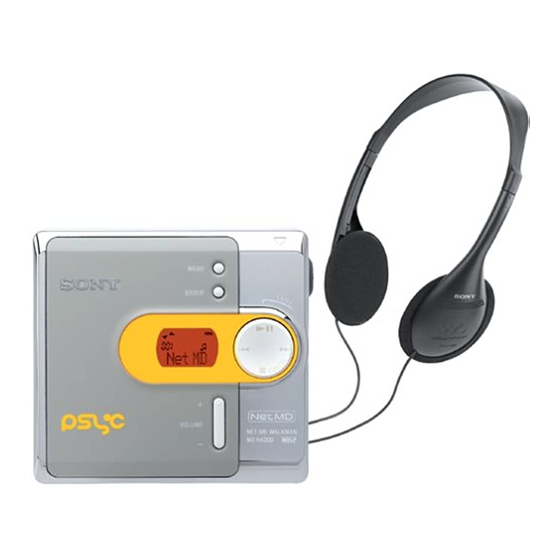
Sony MZ-N420D Service Manual
Hide thumbs
Also See for MZ-N420D:
- Operating instructions manual (56 pages) ,
- Specifications (2 pages) ,
- Specifications (2 pages)
Table of Contents
Advertisement
Quick Links
SERVICE MANUAL
Ver 1.0 2004.04
US and foreign patents licensed from Dolby
Laboratories.
• SonicStage, OpenMG and the OpenMG
logo, MagicGate, Memory Stick and the
MagicGate Memory Stick logo,
Memory Stick and the Memory Stick
logo, Net MD and the Net MD logo are
trademarks of Sony Corporation.
• Microsoft, Windows, Windows NT and
Windows Media are trademarks or
registered trademarks of Microsoft
Corporation in the United States and /or
other countries.
• IBM and PC/AT are registered
trademarks of International Business
Machines Corporation.
• Macintosh is a trademark of Apple
Computer, Inc. in the United States and/
or other countries.
• MMX and Pentium are trademarks or
registered trademarks of Intel
Corporation.
• All other trademarks and registered
trademarks are trademarks or registered
trademarks of their respective holders.
• ™ and ® marks are omitted in this
manual.
Sony Corporation
9-877-707-01
2004D1678-1
Personal Audio Company
© 2004.04
Published by Sony Engineering Corporation
MZ-N420D
Model Name Using Similar Mechanism
Mechanism Type
Optical Pick-up Name
SPECIFICATIONS
Audio playing system
MiniDisc digital audio system
Laser diode properties
Material: GaAlAs
Wavelength: λ = 790 nm
Emission duration: cont inuous
Laser output: less than 44.6 µW
(This output is the value measured at a distance
of 200 mm from the objective lens surface on
the optical pick-up block with 7 mm aperture.)
Recording and playback time (when
using MDW-80)
Maximum 160 min. in monaural
Maximum 320 min. in LP4 stereo
Revolutions
Approx. 380 rpm to 2,700 rpm
Error correction
ACIRC (Advanced Cross Interleave Reed
Solomon Code)
Sampling frequency
44.1 kHz
Coding
ATRAC (Adaptive TRansform Acoustic
Coding)
ATRAC3 — LP2/LP4
PORTABLE MINIDISC PLAYER
US Model
Canadian Model
E Model
MZ-NE410
MT-MZN710-177
LCX-5R
– Continued on next page –
Advertisement
Table of Contents

Related Manuals for Sony MZ-N420D


Summary of Contents for Sony MZ-N420D
- Page 1 • ™ and ® marks are omitted in this 44.1 kHz manual. Coding ATRAC (Adaptive TRansform Acoustic Coding) ATRAC3 — LP2/LP4 – Continued on next page – PORTABLE MINIDISC PLAYER Sony Corporation 9-877-707-01 2004D1678-1 Personal Audio Company © 2004.04 Published by Sony Engineering Corporation...
- Page 2 5 minutes each) 5 minutes each) 5 minutes each) When using a new Sony LR6 (size AA) “STAMINA” alkaline dry battery (produced in Japan). Measured in accordance with the JEITA (Japan Electronics and Information Technology Industries Association) standard. The numbers of tracks that can be checked out differs according to the computer’s operating environment.
-
Page 3: Table Of Contents
MZ-N420D TABLE OF CONTENTS CAUTION 1. SERVICING NOTES ............4 Use of controls or adjustments or performance of procedures other than those specified herein may result in hazardous ra- 2. GENERAL ................5 diation exposure. 3. DISASSEMBLY Notes on chip component replacement 3-1. -
Page 4: Servicing Notes
MZ-N420D SECTION 1 SERVICING NOTES NOTES ON HANDLING THE OPTICAL PICK-UP Providing the required system environment BLOCK OR BASE UNIT System requirements The laser diode in the optical pick-up block may suffer electro- static break-down because of the potential difference generated The following system environment is required in order to use the SonicStage Ver.2.0/MD... -
Page 5: General
MZ-N420D SECTION 2 GENERAL This section is extracted from instruction manual. This model comes in two designs with different shapes and names for the buttons. Front of the player On the following pages of this manual, explanations are given using the illustration in the top-left of this page. -
Page 6: Disassembly
MZ-N420D SECTION 3 DISASSEMBLY • This set can be disassembled in the order shown below. 3-1. CASE (LOWER) (Page 7) In order to remove mechanism deck, please remove MAIN board and upper panel section. 3-2. UPPER PANEL SECTION 3-4. MAIN BOARD... -
Page 7: Case (Lower)
MZ-N420D Note: Follow the disassembly procedure in the numerical order given. 3-1. CASE (LOWER) 2 two screws (M1.4) 1 two screws (M1.4) 3 Remove the case (lower) in the direction of the arrow. 3-2. UPPER PANEL SECTION 1 flexible board... -
Page 8: Lcd Module, Button (Control)
MZ-N420D 3-3. LCD MODULE, BUTTON (CONTROL) 1 four screws 2 two claws 3 LCD module 4 two screws 5 open locker 6 button (control) case (upper) sub assy 3-4. MAIN BOARD 1 Remove two solders of the flexible board (over write head). -
Page 9: Mechanism Deck (Mt-Mzn710-177)
MZ-N420D 3-5. MECHANISM DECK (MT-MZN710-177) 1 step screw (MD) 3 mechanism deck (MT-MZN710-177) The portion which projected is removed. 3-6. SET CHASSIS ASSY 2 two screws (TP 1.7 × 2.5) 4 ground spring (USB) 5 set chassis assy 3 battery case... -
Page 10: Op Service Assy (Lcx-5R)
MZ-N420D 3-7. OP SERVICE ASSY (LCX-5R) 2 gear (SA) 5 screw (M1.4) 1 washer (0.8-2.5) 6 thrust detent spring 3 screw (M1.4) 8 Pull off lead screw. 4 rack spring 9 Opening the over write head toward the direction A , remove the OP service assy (LCX-5R) toward the direction B . -
Page 11: Holder Assy
MZ-N420D 3-8. HOLDER ASSY 5 holder assy 2 Open the holder assy. 4 boss 1 convex portion 3 boss 3-9. DC MOTOR (SLED) (M602) 2 washer (0.8-2.5) 3 gear (SA) 4 two screws (M1.4) 1 Remove six solders of the motor flexible board. -
Page 12: Dc Motor (Over Write Head Up/Down) (M603)
MZ-N420D 3-10. DC MOTOR (OVER WRITE HEAD UP/DOWN)(M603), DC SSM18B MOTOR (SPINDLE) (M601) 1 Remove six solders of the motor flexible board. 2 tapping screw 3 motor cover 7 DC motor (over write head up/down) (M603) Note: Press-fit the gear (HA) up to the position of the DC motor (over write head up/down) (M603) as shown below. -
Page 13: Test Mode
MZ-N420D SECTION 4 TEST MODE Outline Operation in Setting the Test Mode • This set provides the Overall adjustment mode that allows CD • When the test mode becomes active, first the display check mode and MO discs to be automatically adjusted when in the test mode. - Page 14 MZ-N420D Configuration of Test Mode [VOLUME +] key: 100th place of item [Major item switching] number increase. [Test Mode $Display Check Mode%] [VOLUME --] key: 100th place of item number decrease. > x/CANCEL Press the > [Manual Mode] [VOLUME +]...
- Page 15 MZ-N420D [MENU] 5. The display changes a shown below each time the Overall Adjustment Mode key is pressed. Mode to adjust the servo automatically in all items. Normally, automatic adjustment is executed in this mode at the repair. • Address & Adjusted Value Display For further information, refer to “SECTION 5 ELECTRICAL...
- Page 16 MZ-N420D • Description of Error Indication Codes Problem Indication code Meaning of code Simple display Description No error No error No error Illegal access target Adrs Attempt to access an abnormal address address was specified Servo system error High temperature...
- Page 17 MZ-N420D Sound Skip Check Result Display Mode • Cause of Sound Skip Error This set can display the count of errors that occurred during the Cause of error Description of error recording/playing for checking. Sound error correction error • Setting Method of Sound Skip Check Result Display...
-
Page 18: Electrical Adjustments
TDYS-1 R e s e t ! (Part No. : 4-963-646-01) • SONY MO disc available on the market 4. Press the x/CANCEL key to quit the manual mode, and • Digital voltmeter return to the test mode (display check mode). - Page 19 MZ-N420D • Adjustment Method of VC1_LOW (PB) • Adjustment Method of VC2_LOW (item number: 741) (item number: 743) Set LCD display Set LCD display A D * * A D * * ** : Adjusted value ** : Adjusted value 1.
- Page 20 MZ-N420D • Adjustment Method of REG1 • Adjustment Method of REG3_LOW2 (item number: 745) (item number: 748) Set LCD display Set LCD display A D * * A D * * ** : Adjusted value ** : Adjusted value 1. Connect a digital voltmeter to the TP1907 (REGO3) on the [VOLUME +] 1.
- Page 21 MZ-N420D • Adjustment Method of VREC_LOW (X2 speed) • Adjustment Method of VREC_HIGH (HEAD MOTOR) (item number: 751) (item number: 753) Set LCD display Set LCD display A D * * A D * * ** : Adjusted value ** : Adjusted value 1.
- Page 22 MZ-N420D Adjustment/checking and Connection Location: MAIN BOARD (SIDE B) W601 W602 I C 6 5 1 IC601 TP1620(VREC) TP1909(REGO1) TP1915 IC901 IC852 IC501 ( T E S T ) IC801 W 9 0 3 BATT-(GND) TP1928(VCO1) TP1905(VOUT) TP1907(REGO3) TP1655...
- Page 23 MZ-N420D Power Supply Adjustment Auto Item Feed 5. Connect a digital voltmeter to the measuring points on the [VOLUME +] MAIN board, and adjust the voltage with the [VOLUME --] Note: This mode is available to perform the temperature correction and key.
- Page 24 MZ-N420D Laser Power Check 9. Check that the laser power meter reading is 4.95 ± 0.59 mW. 10. Press the key, and set the laser MO (X4 speed) write > Note: If result of measurement of the laser power does not satisfy the specification, either replace the OP (optical pick-up unit) or check check mode (item number 014).
- Page 25 MZ-N420D • Adjustment Method of CD and MO Overall Adjustment 8. If OK through the MO overall adjustments, press the Mode key to return to the test mode and terminate the x/CANCEL 1. Set the test mode (see page 13).
- Page 26 MZ-N420D 2. MO overall adjustment items Item No. Description Item No. Description Focus gain adjustment VC,VR power supply H/L selection Tracking gain adjustment R_GRV setting . servo OFF TWPP gain adjustment Low reflection electrical offset adjustment TWPP offset adjustment 1 Laser ON .
- Page 27 MZ-N420D Remuse Clear Perform the Resume clear when all adjustments completed. • Resume Clear Setting Method 1. Select the manual mode of the test mode, and set item number 043 (see page 14). Set LCD display # # # S 0 0 ### : Address 2.
- Page 28 MZ-N420D Rewriting the Patch Data at Replacement of MAIN Board This set requires the patch data in the nonvolatile memory (IC852) to be rewritten using the application, when the MAIN board was replaced. Caution: The application that meets the microcomputer version in this set must be used when rewriting the patch data. Rewriting the patch data using the application not suitable for the microcomputer version could cause the set to malfunction.
- Page 29 MZ-N420D 5. Confirm that the model and version indicated on the title bar coincide with the codes displayed in the Device Name block and the Version block in the window. 6. Click the [Write + Read] button. The patch data writing and the verify processing will be executed automatically in the following order:...
- Page 30 MZ-N420D • Confirmation of contents of the patch data rewrited 1. Click the [READ] button to confirm the contents of the patch data rewrited. 2. The application reads out the front and reverse patch areas and displays the results in the edit box.
- Page 31 MZ-N420D • Disconnecting the USB cable Disconnect the USB cable as the following procedure after rewriting the patch data and confirmation. Note : When the following procedure is not completed but USB cable is extracted, the application does not recognize the set at exchanging of the set.
- Page 32 MZ-N420D Rewriting the NV values Caution: The application that meets the microcomputer version in this set must be used when rewriting the NV values. Rewriting the NV values using the application not suitable for the microcomputer version could cause the set to malfunction.
- Page 33 MZ-N420D 5. Confirm that the model and version indicated on the title bar coincide with the codes displayed in the Device Name block and the Version block in the window. 6. Click the [Write + Verify] button. The NV values writing and the verify processing will be executed automatically in the following order:...
- Page 34 MZ-N420D 7. The operation will terminate with “Compere OK” given to all areas. If “Compere NG” is given to any area, the nonvolatile memory will be faulty. 8. Click the [USB DISCONNECT] button.
- Page 35 MZ-N420D 9. Confirm that the window becomes as shown below where the [Write + Verify] button is inactive. 10. Disconnect the USB cable from the personal computer and the set.
-
Page 36: Diagrams
MZ-N420D SECTION 6 DIAGRAMS NOTE FOR PRINTED WIRING BOARD AND SCHEMATIC DIAGRAMS Note on Printed Wiring Board: Note on Schematic Diagram: • All capacitors are in µF unless otherwise noted. (p: pF) • X : parts extracted from the component side. - Page 37 MZ-N420D MEMO • Waveforms IC501 9 (RFO)(TP1517) IC601 4 (CLK) IC901 yd (CLK) 2.4Vp-p 2.4Vp-p 5.67 µ s 5.67 µ s 1.2Vp-p 1V/DIV, 2 µ s/DIV 1V/DIV, 2 µ s/DIV 500mV/DIV, 200ns/DIV IC501 rd (TE)(SL501) IC801 2 (OSCO) (at the point of R806) 580mVp-p 44.3ns...
-
Page 38: Block Diagram
MZ-N420D 6-1. BLOCK DIAGRAM SYSTEM CONTROLLER SYSTEM CONTROLLER HP AMP DIGITAL SIGNAL PRCESSOR RF AMP DIGITAL SIGNAL PRCESSOR POWER AMP IC371 IC501 IC801(1/2) IC801(2/2) IC901 REGO1 UNREG OPTICAL PICK-UP DVCC REGO1 IFVDD0 DATA SDO0 AOUT L L IN REGO1 BLOCK... -
Page 39: Printed Wiring Board - Main Board (Side A)
MZ-N420D 6-2. PRINTED WIRING BOARD – MAIN BOARD (SIDE A) – :Uses unleaded solder. MAIN BOARD (SIDE A) • Semiconductor Location Ref. No. Location D171 D271 D606 D607 D903 IC371 IC701 Q501 Q603 Q604 Q605 S803 LCX-5R (OPEN/CLOSE) IC371 IC701... -
Page 40: Printed Wiring Board - Main Board (Side B)
MZ-N420D 6-3. PRINTED WIRING BOARD – MAIN BOARD (SIDE B) – :Uses unleaded solder. When IC852 is damaged, replace the MAIN board. MAIN BOARD (SIDE B) SWITCH OVER WRITE HEAD & LCD MODULE W601 W602 IC651 IC601 (VREC) (REG01) J304... -
Page 41: Schematic Diagram - Main Board (1/4)
MZ-N420D 6-4. SCHEMATIC DIAGRAM – MAIN BOARD (1/4) – • See page 46, 48 for IC Block Diagrams. • See page 37 for Waveforms. C630 C631 47 4V Q605 CPH5614-TL-E D606 MA2YD1700LS0 C632 100p D607 MA2YD1700LS0 Q604 W602 MCH6616-TL-E W601... -
Page 42: Schematic Diagram - Main Board (2/4)
MZ-N420D 6-5. SCHEMATIC DIAGRAM – MAIN BOARD (2/4) – • See page 45, 47 for IC Block Diagrams. • See page 37 for Waveforms. C513 C524 0.022 TP1539 C517 0.01 TP518 R511 CN501 C535 C526 C718 C720 TP1504 0.047 TP1507... -
Page 43: Schematic Diagram - Main Board (3/4)
MZ-N420D 6-6. SCHEMATIC DIAGRAM – MAIN BOARD (3/4) – • See page 49 for IC PIN FUNCTION DESCRIPTION. • See page 37 for Waveforms. R821 R822 R824 220k 470k FB802 R826 C819 2.2k R837 R858 C841 R835 X802 0.001 R827 4.7k... -
Page 44: Schematic Diagram - Main Board (4/4)
MZ-N420D 6-7. SCHEMATIC DIAGRAM – MAIN BOARD (4/4) – • See page 45 for IC Block Diagrams. When IC852 is damaged, replace the MAIN board. not used J304 W901 R312 CN872 TP1882 TP1883 C399 TP1884 TP1885 D271 02DZ2.4-Z(TPH3) TP1886 TP1887 D171 02DZ2.4-Z(TPH3) -
Page 45: Ic Block Diagrams
MZ-N420D • IC BLOCK DIAGRAMS IC371 NJM2776RB2A(TE2) OUT R OUT L IN R IN L STB_TC BIAS X_MUTE VREF VREF AMP IC501 SN761058AZQLR AVCC PEAK/ OFTRK T-ON BOTM 42 FE ABCD 41 ABCD 40 RFI A GND 39 ASSY OFC-C1... - Page 46 MZ-N420D IC601 SC111292EPR2 VC2 VG OUTPUT SW OUTPUT SW CHARGE CHARGE PUMP 1 PUMP 2 VC VG DC IN HI-BRIDGE CHARGE PRE DRIVER PRE DRIVER MONITOR VREF VREF X2/X4 BATM BUFFER DC IN CVREF CONTROL CONTROL CHARGE CHGSW DW BT...
- Page 47 MZ-N420D IC701 SC111290EPR2 48 47 46 45 52 51 3Phase BIAS control 3Phase control PGNDW2 VG VC PGNDW1 VMVW2 3Phase Pre driver WMVW1 3Phase Pre driver PGNDUV2 PGNDUV1 35 UO2 VMU2 VMR2 VMU1 VG VC VMR1 H-BRIDGE PGND2 DRIVER H-BRIDGE...
- Page 48 MZ-N420D IC901 SC11291EPR2 (HP AMP) AMP1 CONTROL BANDGAP FFCLR1 48 VREF REFERENCE XWAKE4 47 REGC3 REF1 XWAKE3 46 REGC2 REF2 REF3 XWAKE2 45 REGC1 REF4 REF5 XWAKE1 44 REGI1 SERIES PASS REGULATOR1 REF3 VRMC 43 REGO1 FFCLR 42 VC2 SERIES PASS...
-
Page 49: Ic Pin Function Description
MZ-N420D • IC PIN FUNCTION DESCRIPTION • IC801 CXD2680-207GA (SYSTEM CONTROLLER, DIGITAL SIGNAL PROCESSOR) Pin No. Pin Name Description OSCI Resonator connection terminal for the system clock (22.5792MHz) OSCO Resonator connection terminal for the system clock (22.5792MHz) VREFL Reference voltage terminal connected to the capacitor (for the built-in D/A converter L-CH) - Page 50 MZ-N420D Pin No. Pin Name Description ADDT Data input from the external A/D converter (fixed at “L” in this set) KRCK L/R sampling clock (44.1KHz) output to the external A/D converter Not used (open) XBCK Bit clock (2.8224MHz) output to the external A/D converter Not used (open) FS256 11.2896MHz clock output...
- Page 51 MZ-N420D Pin No. Pin Name Description BATT_CTL Control signal output for the voltage step up circuit in the external battery case Not used (open) VREC_CTL VREC voltage control signal output Not used (open) XRST_CHG_IC Reset signal output to the battery charge control IC Not used (open)
- Page 52 MZ-N420D Pin No. Pin Name Description HIDC_MON HIGH DC voltage monitor input (A/D input) Not used (fixed at “H”) WK_DET Set key WAKE detection signal input BATT_MON External battery voltage monitor input Not used (fixed at “H”) HALF_LOCK_SW Open button detection switch input (A/D input) “L” : the open button is pressed...
- Page 53 MZ-N420D Pin No. Pin Name Description — DRAM chip select terminal Not used (open) — DRAM clock terminal Not used (open) — DRAM clock enable terminal Not used (open) UDQM — DRAM byte mask terminal Not used (open) LDQM —...
- Page 54 MZ-N420D Pin No. Pin Name Description FVDD0 — Power supply terminal (for the built-in flash memory) FVSS0 — Ground terminal (for the built-in flash memory) 301, 302 DVDD5, 6 — Power supply terminal 303, 304 DRAMVDD3, 4 — Power supply terminal (for DRAM) MSAK —...
-
Page 55: Exploded Views
MZ-N420D SECTION 7 EXPLODED VIEWS NOTE: • -XX, -X mean standardized parts, so they may • Color Indication of Appearance Parts The components identified by mark 0 or have some differences from the original one. Example: dotted line with mark 0 are critical for safety. -
Page 56: Chassis Section
MZ-N420D 7-2. CHASSIS SECTION mechanism deck section-1 (MT-MZN710-177) not supplied main board section Ref. No. Part No. Description Remarks Ref. No. Part No. Description Remarks 3-237-072-02 SCREW (MD), STEP 3-318-382-91 SCREW (1.7X2.5), TAPPING 3-238-876-07 SCREW (M1.4), TOOTHED LOCK 3-246-245-02 SLIDER, OPEN... -
Page 57: Main Board Section
MZ-N420D 7-3. MAIN BOARD SECTION Ref. No. Part No. Description Remarks Ref. No. Part No. Description Remarks 3-246-247-04 CASE, BATTERY 3-237-074-11 TERMINAL (-), BATTERY 3-237-073-01 TERMINAL BOARD (+), BATTERY MAIN BOARD, COMPLETE... -
Page 58: Mechanism Deck Section-1 (Mt-Mzn710-177)
MZ-N420D 7-4. MECHANISM DECK SECTION-1 (MT-MZN710-177) mechanism deck section-2 (MT-MZN710-177) not supplied Ref. No. Part No. Description Remarks Ref. No. Part No. Description Remarks X-3381-219-4 HOLDER ASSY 3-043-237-02 BEARING (N) 3-224-779-02 SPRING, THRUST DETENT 4-222-203-02 SCREW, LEAD 3-225-996-01 SCREW (M1.4)(EG),PRECISION PAN... -
Page 59: Mechanism Deck Section-2 (Mt-Mzn710-177)
MZ-N420D 7-5. MECHANISM DECK SECTION-2 (MT-MZN710-177) M602 M603 supplied M601 Ref. No. Part No. Description Remarks Ref. No. Part No. Description Remarks 3-225-278-12 SCREW, TAPPING 3-235-839-02 LEVER (RACK) 3-235-838-02 COVER, MOTOR 3-338-645-31 WASHER (0.8-2.5) 3-235-836-01 GEAR (HB) 4-222-222-01 GEAR (RACK) -
Page 60: Electrical Parts List
MZ-N420D SECTION 8 MAIN ELECTRICAL PARTS LIST NOTE: • Due to standardization, replacements in the • RESISTORS When indicating parts by reference number, parts list may be different from the parts All resistors are in ohms. please include the board name. - Page 61 MZ-N420D MAIN Ref. No. Part No. Description Remarks Ref. No. Part No. Description Remarks C808 1-164-937-11 CERAMIC CHIP 0.001uF 10.00% 50V C984 1-164-937-11 CERAMIC CHIP 0.001uF 10.00% 50V C811 1-125-837-91 CERAMIC CHIP 6.3V C985 1-125-777-11 CERAMIC CHIP 0.1uF 10.00% 10V...
- Page 62 MZ-N420D MAIN Ref. No. Part No. Description Remarks Ref. No. Part No. Description Remarks L904 1-416-669-11 INDUCTOR 22uH R654 1-218-990-11 SHORT CHIP R655 1-218-953-11 RES-CHIP 1/16W < LINE FILTER > R656 1-218-985-11 RES-CHIP 470K 1/16W LF952 1-416-405-21 FERRITE R657 1-218-990-11 SHORT CHIP...
- Page 63 MZ-N420D MAIN Ref. No. Part No. Description Remarks R858 1-218-990-11 SHORT CHIP R860 1-216-864-11 METAL CHIP 1/16W R861 1-218-990-11 SHORT CHIP R862 1-218-989-11 RES-CHIP 1/16W R863 1-218-990-11 SHORT CHIP R871 1-218-957-11 RES-CHIP 2.2K 1/16W R872 1-218-953-11 RES-CHIP 1/16W R873 1-218-985-11 RES-CHIP...
- Page 64 MZ-N420D REVISION HISTORY Clicking the version allows you to jump to the revised page. Also, clicking the version at the upper right on the revised page allows you to jump to the next revised page. Ver. Date Description of Revision...
Need help?
Do you have a question about the MZ-N420D and is the answer not in the manual?
Questions and answers