E.F. Johnson Company 5100 Series Service Manual
Hide thumbs
Also See for 5100 Series:
- Operating manual (34 pages) ,
- Service manual (39 pages) ,
- Assembly and test procedures (36 pages)
Table of Contents
Advertisement
Quick Links
Download this manual
See also:
Operating Manual
5100 S
ERIES
P
R
ORTABLE
APCO Project 25
– Conventional
– Trunked
SMARTNET
SmartZone
®
Analog FM
Conventional
VHF
1 and 5 Watts
UHF
1 and 4 Watts
700 MHz
1 and 2.7 Watts
800 MHz
1 and 3 Watts
7.2 VDC
Part No. 242-51xx-xxx
DIGITAL/ANALOG PORTABLE RADIO
ADIO
/
®
SERVICE
MANUAL
Part Number: 001-5100-0017CD
December 2004
Supersedes: 001-5100-0016CD; 8/04
Advertisement
Table of Contents

Related Manuals for E.F. Johnson Company 5100 Series


Summary of Contents for E.F. Johnson Company 5100 Series
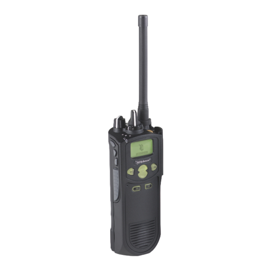
- Page 1 SERVICE MANUAL DIGITAL/ANALOG PORTABLE RADIO 5100 S ERIES ORTABLE ADIO APCO Project 25 – Conventional – Trunked SMARTNET ® SmartZone ® Analog FM Conventional 1 and 5 Watts 1 and 4 Watts 700 MHz 1 and 2.7 Watts 800 MHz 1 and 3 Watts 7.2 VDC Part No.
- Page 2 51xx SERIES PORTABLE VHF, UHF, 700/800, 800 MHz PROJECT 25 CONVENTIONAL AND TRUNKED ANALOG CONVENTIONAL ® ® SMARTNET /SMARTZONE 7.5 VDC 5W (VHF), 4W (UHF), 2.5W (700 MHz) 3W (800 MHz) Part No. 242-51xx-xx0 Copyright© 2004 by the EFJohnson Company The EFJohnson Company, which was founded in 1923, provides wireless communication systems solutions for public safety, government, and commercial customers.
-
Page 3: Table Of Contents
TABLE OF CONTENTS TABLE OF CONTENTS GENERAL INFORMATION TRANSCEIVER PROGRAMMING SCOPE OF MANUAL ....1-1 PROGRAMMING SETUP ....4-1 RADIO DESCRIPTION . - Page 4 TABLE OF CONTENTS TABLE OF CONTENTS (CONT’D) Transmit Signal Path ..... 5-21 VHF RF Board Version B ADSIC (U2)......5-21 Schematic.
- Page 5 TABLE OF CONTENTS TABLE OF CONTENTS (CONT’D) LIST OF TABLES 5100-160 Logic Board Version B Schematic ......9-9 Board Layout .
-
Page 6: General Information
UHF Mid: 403-470 MHz ming, alignment, and service information for the UHF High: 450-512 MHz EFJohnson 5100 series portable radio. 700/800 MHz: 762-806 and 806-870 MHz 800 MHz: 806-870 MHz (see next section) The 51SL and Ascend (Multi-Net) models are... -
Page 7: Operating Protocols
GENERAL INFORMATION used in systems where the channel spacing is 25 kHz Systems or 30 kHz. A system is a collection of channels or talk Digital - C4FM modulation is used. The voice is digi- groups belonging to the same repeater site. It defines tized, filtered, error corrected, optionally encrypted, all the parameters and protocol information required to and then transmitted. -
Page 8: Programming
GENERAL INFORMATION Zones M (Model) 1 - 5100 series A zone is a collection of up to 16 channels of any 2 - 51SL series type. For example, a zone could include 12 conven- 5 - Ascend series tional channels and 4 SMARTNET channels. One use... -
Page 9: Transceiver Identification
GENERAL INFORMATION function of PCConfigure to determine which proto- NOTE: Emergency 24-hour technical support is also cols and options are enabled in your radio (see available at the 800 and preceding numbers during off Section 4). hours, holidays, and weekends. D Encryption Hardware (see Section 1.13.2) When your call is answered at the EFJohnson 1 - No encryption hardware (software encryp) -
Page 10: Accessories
GENERAL INFORMATION Table 1-1 Accessories Table 1-1 Accessories (Continued) Accessory Part No. Accessory Part No. Batteries 585-5100-130 2.5” D-swivel belt loop only 3600 mAH NiMH standard 587-5100-360 585-5100-132 3.0” D-swivel belt loop only 3600 mAH NiMH std intrin safe 587-5100-361* Radio D-swiv button for -130/-132 loops 585-5100-127 Battery case for AA alkaline 250-5100-280... -
Page 11: Replacement Parts
GENERAL INFORMATION When returning equipment for repair, it is also 1.11 INTRINSICALLY SAFE INFORMATION recommended that you use a PO number or some other reference number on your paperwork in case you need 1.11.1 INTRODUCTION to call the repair lab about your unit. These numbers are referenced on the repair order and make it easier Intrinsically safe 5100 transceivers have been and faster to locate your unit in the lab. -
Page 12: Possible Ignition Sources
GENERAL INFORMATION cient electrical and thermal energy under normal oper- specified in the testing procedure occur. In other ation or specified fault conditions per the testing words, it must be able to withstand two simultaneous standard to cause ignition of a specific flammable or unrelated breakdowns without causing ignition. -
Page 13: Secure Communication
GENERAL INFORMATION include combustible dusts, and Class III materials ceiver. These protocols digitize the voice and then include ignitable fibers or flyings. The typical hazard- encrypt it using the DES or AES algorithm and an ous materials in each group and class are shown in encryption key. -
Page 14: Radio Hardware Changes
GENERAL INFORMATION . y l " r " B , ) r t a l t a l o i t o i t a l i a l i a l i a l i Figure 1-1 Hardware Changes Flowchart 1.13 RADIO HARDWARE CHANGES Version B - The changeover to this version occurred starting in late 2003. -
Page 15: Logic And Ui Board Changes
GENERAL INFORMATION The Revision Letter in the radio identification 1.13.2 LOGIC AND UI BOARD CHANGES number (see Section 1.5) can be used to determine if a VHF radio has this new Version B board. Radios with As shown in Figure 1-1 and Table 1-4, there have a Revision Letter of “B”... -
Page 16: 51Xx Family Logic And Firmware Versions
GENERAL INFORMATION Table 1-4 51xx Family Logic and Firmware Versions Analog Channel Digital Channel Application Encryption Encryption Logic/Radio Version [1] (Firmware) Code Base DES-XL DES-OFB Version 1 (No Module/Software Encryption) 1.xx Current standard version which uses the -110 Logic board and -410 UI Board. Not FIPS approved. Version 2 (uses EFJ SEM module) 2.xx Current version which has the EFJohnson SEM... - Page 17 GENERAL INFORMATION 5100 PORTABLE SPECIFICATIONS The following are general specifications intended for use in testing and servicing this transceiver. For current advertised specifications, refer to the specification sheet available from your sales representative. Values are typical and are subject to change without notice. GENERAL Frequency Range VHF: 136-174 MHz...
-
Page 18: Battery, Accessory, And Disassembly Information
BATTERY, ACCESSORY, AND DISASSEMBLY INFORMATION SECTION 2 BATTERY, ACCESSORY, AND DISASSEMBLY INFORMATION Battery Release Button Figure 2-1 Battery Removal 2.1 BATTERY INFORMATION Do not expose the charger base to high level RF signals while a battery is being charged because this 2.1.1 BATTERY REMOVAL/INSTALLATION may cause a charger fuse to blow (especially in the UHF range). -
Page 19: Battery Care
BATTERY, ACCESSORY, AND DISASSEMBLY INFORMATION 2.1.4 BATTERY CARE fails to hold a charge or provides only a very short operating time, it must be replaced with a new unit. WARNING: Do not incinerate a battery pack because it may explode. Also, do not short circuit the terminals A fully charged battery provides approximately because the battery pack and the object causing the 13 hours of service before recharging is required. -
Page 20: Accessory Installation
BATTERY, ACCESSORY, AND DISASSEMBLY INFORMATION Install Lock Screw Here Accessory Connector Latch Hook Figure 2-3 Accessory Installation 2.3 ACCESSORY INSTALLATION Option Select Lines To connect an accessory such as a speaker- Opt Sel 1 (pin 1) and Opt Sel 2 (pin 5) of the microphone to the transceiver, refer to Figure 2-3 and UDC (accessory) connector indicate to the control proceed as follows:... -
Page 21: Transceiver Disassembly
BATTERY, ACCESSORY, AND DISASSEMBLY INFORMATION 2.4 TRANSCEIVER DISASSEMBLY 2.4.1 SEPARATING FRONT COVER AND CHASSIS 1. Remove the antenna. 2. Insert a small flat-blade screwdriver or similar tool between the plastic front cover and metal chassis as shown below. Carefully lift the chassis out of the cover with the screwdriver blade. Raise it to approximately the point shown in the next illustration. -
Page 22: Removing Rf And Logic Boards From Chassis
BATTERY, ACCESSORY, AND DISASSEMBLY INFORMATION 2.4.2 REMOVING RF AND LOGIC BOARDS FROM CHASSIS 1. Separate the front cover and chassis as described in the preceding section. The RF and logic boards are located inside the metal chassis as shown below. Logic Board RF Board 2. -
Page 23: Removing Ui (User Interface) Board
BATTERY, ACCESSORY, AND DISASSEMBLY INFORMATION 2.4.3 REMOVING UI (USER INTERFACE) BOARD 1. Separate the front cover and chassis as described in Section 2.4.1. The UI board is located inside the front cover as shown below. Microphone UI Board Unsolder Wires Remove Unlock Screws... -
Page 24: Removing Switch Assembly
BATTERY, ACCESSORY, AND DISASSEMBLY INFORMATION 2.4.4 REMOVING SWITCH ASSEMBLY 1. Separate the front cover and chassis as described in Section 2.4.1. Then remove the UI board as described in the preceding section. 2. Pull the rubber knobs and plastic channel number ring off the shafts. 3. -
Page 25: Operation
OPERATION SECTION 3 OPERATION 3.1 GENERAL The operation of the 5100 transceiver is included in a separate manual that is included on the CD-ROM with this manual. -
Page 26: Transceiver Programming
CD-ROM with the service manual. NOTE: The -920 cable, -488 software, and a CD manual are included in the 5100 Series Programming Kit, Part No. 250-5100-003. 4.2 COMPUTER DESCRIPTION Tone (CTCSS) and digital (DCS) Call Guard... -
Page 27: Cloning Procedure
TRANSCEIVER PROGRAMMING 4.4 CLONING PROCEDURE For more information on cloning one radio with another, refer to Section 14 of the PCConfigure The Clone feature allows one radio to be used to Manual included on the CD-ROM with this service program another with identical information. The manual. -
Page 28: Circuit Description
RS-232 communications 5.1.1 INTRODUCTION between the radio and remote computer stations for the purposes of radio programming, tuning, encryption key The EFJohnson 5100 series digital portable radio loading and software downloading. ® uses a PowerPC -based controller and a Digital Signal... -
Page 29: Project 25 Digital Mode
CIRCUIT DESCRIPTION VHF RF BOARD (VERSION C) Transmit Mode This bit stream in then encoded, two bits at a time, into a digital level corresponding to one of the The signal from the microphone is amplified and four allowable frequency deviations. This produces then routed to the CODEC chip where it is first digi- 16-bit symbols with a rate of 4800 Hz. -
Page 30: Vhf Rf Board Block Diagram (Version C)
CIRCUIT DESCRIPTION VHF RF BOARD (VERSION C) RF / Logic Interface 64.455 MHz BPF 1 BPF 2 1Kbit EEPROM MOSI RFOut 15 kHz 15 kHz MISO Receiver Back End Addr1 SPI Addr 136 - 174 MHz 8 ch Addr2 200 - 239 MHz Antenna Addr3 D0-D5... -
Page 31: Synthesizer
CIRCUIT DESCRIPTION VHF RF BOARD (VERSION C) IF of 64.455 MHz to a second IF frequency of 2.1 Reference PLL MHz. Phase Locked Loop circuitry inside of the AD9864 operates with a phase-detector frequency The reference PLL phase locks the receive PLL of 15 kHz. -
Page 32: Uhf Rf Board (Version C)
CIRCUIT DESCRIPTION VHF RF BOARD (VERSION C) UHF RF BOARD (VERSION C) applied to the transmit PLL transmit VCO (U47) fixed tuned bandpass filters are used in the front-end provides high-frequency modulation. Signals for both of the receiver. Depending on the desired receive band, modulation ports are provided by DACs on the digital the appropriate filter is selected using RF switches board. -
Page 33: Uhf Rf Board Block Diagram (Version C)
CIRCUIT DESCRIPTION UHF RF BOARD (VERSION C) RF / Logic Interface Bandpass Bandpass Filters Filters 380-444 MHz 380-444 MHz Receiver Back End (450-455 MHz) (450-455 MHz) MGA-71543 IF Amp MIXER 64.455 MHz 64.455 MHz Fif = 2.1MHz AT-267 MOSI 15 KHz BW 15 KHz BW MMBR941 Switch... -
Page 34: Synthesizer
CIRCUIT DESCRIPTION UHF RF BOARD (VERSION C) Analog / Digital Conversion and Processing - A RF2361 buffer amplifier (U6) provides the Sigma-delta converters provide I and Q sampling required level of drive for the receiver mixer's local directly from the second IF frequency. The oscillator signal as discussed above. -
Page 35: 700/800 Mhz Rf Board (Version C)
CIRCUIT DESCRIPTION 700/800 MHz RF BOARD (VERSION C) RF / Logic Interface Bandpas s Filters Receiver Back End (Digital IF) IF Am p Varacter-Tuned 762 - 776 MHz Fif = 2.1MHz MIXER RF2361 Bandpass Filter 64.455 MHz MOSI Switc h MMBR941 Switc h Switc h... -
Page 36: Synthesizer
CIRCUIT DESCRIPTION 700/800 MHz RF BOARD (VERSION C) LNA minimizes the impact of the filter loss on the frequency of 62.355 MHz in order to convert the receiver sensitivity. first IF of 64.455 MHz to a second IF frequency of 2.1 MHz. -
Page 37: Transmitter
CIRCUIT DESCRIPTION 700/800 MHz RF BOARD (VERSION C) RF BOARD OVERVIEW (VERSION A/B) backend IC. The center frequency of this oscillator is corrected using a DC tuning voltage from the digital board during receive and it is modulated with voice or To maintain the specified Transmitter output data during transmit. -
Page 38: Vhf/Uhf Rf Board (Version A/B)
CIRCUIT DESCRIPTION VHF/UHF RF BOARD (VERSION A/B) Figure 5-4 RF Board Block Diagram (Version A/B) The frequency generation function is performed The transmitter consists of an RF PA IC that gets by three ICs and associated circuitry. The reference an injection signal from the VCO. Transmit power is oscillator provides a frequency standard to the synthe- controlled by two custom ICs that monitor the output sizer/prescaler IC which controls the VCO IC. - Page 39 CIRCUIT DESCRIPTION VHF/UHF RF BOARD (VERSION A/B) device (Q202), whereas the VHF Tx VCO’s active circuit. The Tx VCO feedback capacitors are C219 device is a transistor inside the VCO buffer. The UHF and C220. Varactor diode CR203/CR207 sets the Tx Tx VCO uses two active devices, one external (Q203) frequency while varactor CR202 is the Tx modulation and the other internal to the VCO buffer.
-
Page 40: Antenna Switch
CIRCUIT DESCRIPTION VHF/UHF RF BOARD (VERSION A/B) 5.6.2 ANTENNA SWITCH filtered by a second broadband, fixed-tuned, bandpass filter consisting of C6, C7, C8, C80, C86, C87, C88, The antenna switch is a current device consisting C97, C99, L3, L4, L5, and L30 (VHF) or C4 -C7, of a pair of diodes (CR108/ CR109) that electroni- C88 - C94, C99, and L11 - L15 (UHF) to improve the cally steer RF between the receiver and the transmitter. -
Page 41: Transmitter
CIRCUIT DESCRIPTION VHF/UHF RF BOARD (VERSION A/B) filtered, mixed down to baseband, and filtered again. RF Power Amplifier Module The differential output data stream is then sent to the logic board where it is decoded to produce the recov- RF power amplifier module U105 is a wide-band, ered audio. -
Page 42: 800 Mhz Rf Board (Version A/B)
CIRCUIT DESCRIPTION 800 MHz RF BOARD (VERSION A/B) • 5.7 800 MHz RF BOARD (VERSION A/B) For first LO injection frequencies 777-797 MHz, pins 6 and 7 must both be low. NOTE: The following describes the earlier Version A • and B RF boards described in Section 1.13. -
Page 43: Antenna Switch
CIRCUIT DESCRIPTION 800 MHz RF BOARD (VERSION A/B) loop divider's output signal with the signal from diodes CR102 and CR104 must be back-biased to U304 (that is divided down after it is applied to pin properly route the received signal. 14 of U302). -
Page 44: Receiver Back End
CIRCUIT DESCRIPTION 800 MHz RF BOARD (VERSION A/B) capacitor C213. The mixer's LO port is matched to the filters in the ABACUS IC. The ABACUS IC contains radio's PLL by a capacitive tap, C207 and C206. a feedback AGC circuit to expand the dynamic range of the sigma-delta converter. -
Page 45: User Interface Board (All)
CIRCUIT DESCRIPTION UI BOARD (ALL VERSIONS) Q501. Transistor Q501 responds to the base drive level 5.8.3 MEMORY by varying the DC control voltages applied to pin 2 of the RF PA which controls the RIF power level of Early Units (Versions A and B in Section 1.13) module U502. -
Page 46: Logic Board (Version C)
CIRCUIT DESCRIPTION LOGIC BOARD (VERSION C) LOGIC BOARD (VERSION A/B) 5.9.2 DIGITAL SIGNAL PROCESSING 5.10 LOGIC BOARD (VERSION A/B) OVERVIEW NOTE: The following describes the Version A and B The DSP section consists of a DSP chip (U15) logic board described in Section 1.13. and the CODEC (U27). -
Page 47: Receive Signal Path
CIRCUIT DESCRIPTION LOGIC BOARD (VERSION A/B) ADSIC via the serial port. In the ADSIC, the VCO D/ initial programming, the reference clock must be A converts the sampled modulation signal into an present. analog signal and then routes this signal to the VCO on the RF Board. -
Page 48: Transmit Signal Path
CIRCUIT DESCRIPTION LOGIC BOARD (VERSION A/B) AUDIO CIRCUIT (VERSION A/B) 5.10.4 TRANSMIT SIGNAL PATH through a serial port. This serial port consists of pins SCKR, RFS, RxD, TxD, SCKT, and TFS on the The ADSIC contains an analog-to-digital (ADC) ADSIC. converter for the microphone. -
Page 49: Transmit Audio Circuit
CIRCUIT DESCRIPTION AUDIO CIRCUIT (VERSION A/B) Internal U17A RF Board Logic Board UI Board Speaker Amp Tone Sig Tones Buffer 8 ohms U8A/B U17C U17B Audio Mute Single-Diff Diff-Single Combiner Rx Signal Data Converter Switch Converter (SBI/DIN/DIN*/ODC) External ADSIC Mute Speaker Amp Volume Microcontroller... -
Page 50: Alignment Procedure
ALIGNMENT PROCEDURE SECTION 6 ALIGNMENT PROCEDURE 5100 Test Cable DB9 - Connect To Part No. 023-5100-940 Serial Port Audio Out Cable Part No. 023-5100-950 Communication Monitor SINAD Meter/ AC Voltmeter Figure 6-1 Alignment Setup 6.1 GENERAL All adjustments are set digitally using the computer. -
Page 51: Pctune Version Required
ALIGNMENT PROCEDURE Menu Bar Tool Bar Radio Information Tune Category Buttons Adjusts Freq Tuning Instructions Select Next Adjustment Mode/Tool Tip Figure 6-2 PCTune Main Screen (Version 2.0) Software Installation On-Line Help Proceed as follows to install this software: On-line help is currently not available. 1. -
Page 52: Menu Bar Description
ALIGNMENT PROCEDURE - Selects the Partial Tune mode the same as Tuning Categories the Transfer > Tune Partial menu (see Section 6.3.3) This mode allows manual selection of These buttons select the tuning adjustment to be the desired Tune Category and then automati- performed. -
Page 53: Tools Menu
ALIGNMENT PROCEDURE selected. These parameters default to the last selected change the radio series or band or exit an adjustment condition the next time the program is started. before it is complete. Set Band - Selects the operating band of the radio. All tuning values are reset to the factory defaults. -
Page 54: Starting And Configuring Pctune
ALIGNMENT PROCEDURE • Section 4) should not be used because it does not To perform these tests, a Digital Communication have the audio output jack. Analyzer such as Motorola R2670 or IFR 2975 is required. 2. Connect the other end of the test cable to the acces- •... -
Page 55: Transmitter Tests
ALIGNMENT PROCEDURE 2. Set the analyzer output level for 0.35 µV (–116 the receiving radio. This tone can also be used to test dBm) at the receiver antenna jack. The BER (Bit other radios. Error Rate) should be 5% or less. (This is a ratio of the receive bit errors to the total number of bits 7. -
Page 56: Transmitter Performance Tests
ALIGNMENT PROCEDURE Squelch Sensitivity Transmit Frequency 5. Increase the signal generator output from zero and 2. Monitor the transmit frequency and at room temper- note the SINAD when unsquelching occurs. It ature it should ±100 Hz. At other temperatures (–30 should be approximately 8 dB. -
Page 57: Parts List
PARTS LIST SECTION 7 PARTS LIST Ref No. Description Part No. Ref No. Description Part No. VHF 134-174 MHz, Version B 023-5110-001 CHASSIS, HARDWARE, MISC UHF 380-450 MHz, Version B 023-5120-001 UHF 403-470 MHz, Version B 023-5130-001 UHF 450-512 MHz, Version B 023-5140-001 A 030 Rear housing assembly, std version 023-5100-030... -
Page 58: Rf Board (A200)
PARTS LIST CHASSIS, HARDWARE, MISC (Cont’d) LOGIC BOARD (VERSION C) Ref No. Description Part No. Ref No. Description Part No. LOGIC BOARD (A100) MP 030 RF shield, improved Ver A/B bds 017-2229-552 Part No. 023-5500-120 RF shield, Version C RF boards 017-2229-569 (see Section 1.13.1) (Version C, see Section 1.13) - Page 59 PARTS LIST LOGIC BOARD (VERSION C) Ref No. Description Part No. Ref No. Description Part No. C 083 33 pF ±10% 25V cer smd 510-3681-330 CR 004 Switching diode 523-1004-021 C 084 33 pF ±10% 25V cer smd 510-3681-330 CR 006 3.6V zener diode 523-2016-369 C 085 33 pF ±10% 25V cer smd...
- Page 60 PARTS LIST LOGIC BOARD (VERSION C) Ref No. Description Part No. Ref No. Description Part No. R 029 4.7k ohm ±5% 1/16W smd 569-0165-472 R 096 1k ohm ±5% 1/16W smd 569-0165-102 R 030 4.7k ohm ±5% 1/16W smd 569-0165-472 R 097 1k ohm ±5% 1/16W smd 569-0165-102...
-
Page 61: Logic Board (A100)
PARTS LIST LOGIC BOARD (VERSION C) LOGIC BOARD (VERSION A/B) Ref No. Description Part No. Ref No. Description Part No. R 256 10 ohm ±5% 1/16W smd 569-0165-100 C 003 .01 µF ±10% 10V cer smd 510-3681-103 R 257 10 ohm ±5% 1/16W smd 569-0165-100 C 004 .01 µF ±10% 10V cer smd... - Page 62 PARTS LIST LOGIC BOARD (VERSION A/B) Ref No. Description Part No. Ref No. Description Part No. C 045 .01 µF ±10% 10V cer smd 510-3681-103 C 107 10 pF ±.1 pF NPO cer smd 510-3673-100 C 046 .01 µF ±10% 10V cer smd 510-3681-103 C 047 .01 µF ±10% 10V cer smd...
- Page 63 PARTS LIST LOGIC BOARD (VERSION A/B) Ref No. Description Part No. Ref No. Description Part No. R 008 100k ohm ±5% 1/16W smd 569-0165-104 R 044 100 ohm ±5% 1/16W smd 569-0165-101 R 009 220k ohm ±5% 1/16W smd 569-0165-224 R 045 100 ohm ±5% 1/16W smd 569-0165-101...
-
Page 64: User Interface Board (A400)
PARTS LIST LOGIC BOARD (VERSION A/B) USER INTERFACE BOARD (VERSION C) Ref No. Description Part No. Ref No. Description Part No. R 097 100k ohm ±5% 1/16W smd 569-0165-104 C 011 .1 µF ±10% X7R 25V cer smd 510-3675-104 R 098 100k ohm ±5% 1/16W smd 569-0165-104 C 012... - Page 65 PARTS LIST USER INTERFACE BOARD (VERSION C) Ref No. Description Part No. Ref No. Description Part No. C 059 .1 µF ±10% X7R 25V cer smd 510-3675-104 C 105 1.0 µF 16V cer smd 510-3923-105 C 060 .1 µF ±10% X7R 25V cer smd 510-3675-104 C 106 1.0 µF 16V cer smd...
- Page 66 PARTS LIST USER INTERFACE BOARD (VERSION C) Ref No. Description Part No. Ref No. Description Part No. CR 043 LED, green RG1101 smd 549-4003-011 R 014 220k ohm ±5% 1/16W smd 569-0165-224 CR 044 5.6V zener diode 523-2016-569 R 015 20k ohm ±1% 1/16W smd 569-0161-432 R 016...
- Page 67 PARTS LIST USER INTERFACE BOARD (VERSION C) Ref No. Description Part No. Ref No. Description Part No. R 064 220k ohm ±5% 1/16W smd 569-0165-224 R 110 100k ohm ±5% 1/16W smd 569-0165-104 R 065 10k ohm ±5% 1/16W smd 569-0165-103 R 111 100k ohm ±5% 1/16W smd...
-
Page 68: User Interface Board (A400)
PARTS LIST USER INTERFACE BOARD (VERSION C) USER INTERFACE BOARD (VERSION A/B) Ref No. Description Part No. Ref No. Description Part No. R 162 470 ohm ±5% 1/16W smd 569-0165-471 U 009 A/D converter, 10 bit LTC1199 544-2031-005 R 163 470 ohm ±5% 1/16W smd 569-0165-471 U 010... - Page 69 PARTS LIST USER INTERFACE BOARD (VERSION A/B) Ref No. Description Part No. Ref No. Description Part No. C 015 .01 µF ±10% 10V cer smd 510-3681-103 C 064 .01 µF ±10% 10V cer smd 510-3681-103 C 016 .01 µF ±10% 10V cer smd 510-3681-103 C 065 .01 µF ±10% 10V cer smd...
- Page 70 PARTS LIST USER INTERFACE BOARD (VERSION A/B) Ref No. Description Part No. Ref No. Description Part No. C 121 .01 µF ±10% 10V cer smd 510-3681-103 PC 001 PC board, user interface rev 10 035-5100-400 (-410 bd) C 131 .001 µF ±10% 10V cer smd 510-9227-102 PC board, user interface revision 1 035-5100-450 1...
- Page 71 PARTS LIST USER INTERFACE BOARD (VERSION A/B) Ref No. Description Part No. Ref No. Description Part No. R 029 4.7k ohm ±5% 1/16W smd 569-0165-472 R 083 100k ohm ±5% 1/16W smd 569-0165-104 R 030 2k ohm ±5% 1/16W smd 569-0165-202 R 084 47k ohm ±5% 1/16W smd...
- Page 72 PARTS LIST USER INTERFACE BOARD (VERSION A/B) Ref No. Description Part No. Ref No. Description Part No. R 137 220k ohm ±5% 1/16W smd 569-0165-224 R 247 100k ohm ±5% 1/16W smd 569-0165-104 R 138 220k ohm ±5% 1/16W smd 569-0165-224 R 248 82 ohm ±5% 1/16W smd...
-
Page 73: Exploded Views
PARTS LIST EXPLODED VIEWS MP107 MP108 MP106 HW101 MP105 MP006 A050 MP007 MP109 MP114 PC010 HW102 MP115 MP003 MP116 NP101 MP101 MP120 A040 (Complete Assembly) MP111 Front Cover Assembly 7-17... - Page 74 PARTS LIST EP101b MP104 EP102 R101 S101 PC040 MP040 Top Switch Assembly HW031 J030 CH030 MP035 A035 Rear Housing Assembly 7-18...
- Page 75 PARTS LIST A050/A060 DS401 MP401 A400 Short Lead on Top A401 J8/J9 W101 ( - Case) W102 (+) MK101 MP110 SP101 NP102 HW103 MP113 MP112 W103/W104 EP031 7-19...
- Page 76 PARTS LIST A200 MP032 MP030 Part of A200 Part of A200 EP030 MP033 MP031 A030 EP031 MP034 A100 7-20...
-
Page 77: Schematic Diagrams And Component Layouts
SECTION 8 SCHEMATIC DIAGRAMS AND COMPONENT LAYOUTS A400 A100 USER INTERFACE A200 LOGIC BOARD (UI) BOARD PC10 RF BOARD UDC Flex Flex Cir Circuit Opt Sel 1 RF_CLK+ RF_CLK_CPLD HCNTL0 HCNTL0 OPT_SEL1 Ext Spkr + HCNTL1 HCNTL1 EXTSPKR_P Ext Mic RF_DAT+ RF_DATA_CPLD EXT_MIC... -
Page 78: Schematic
A400 USER INTERFACE A100 A215 LOGIC BOARD (UI) BOARD PC10 RF BOARD PC50 UDC Flex Flex Cir Circuit Opt Sel 1 D Out D Out HCNTL0 EB_A29 OPT_SEL1 Ext Spkr + D Out* D Out* HCNTL1 EB_A30 EXTSPKR_P Ext Mic EXT_MIC Sw B+ SW_BATT... - Page 79 +5VR IF FILTER .1uf SHIELD-IF LRG .01uf 390nH 0603 SHIELD-IF SM 180pf 0603 270nH 2% 180pf DSF753 FROM PG 5 68nH 33pf 100pf 1008 .01uf 1008 270nH 2% 270nH 2% 68pf DSF753 0805 10pf 1008 1008 SHIELD-BACKEND 1000pf +5.5V +5.5V +3.3VXR +5VR +5.5V...
- Page 80 UNSW_BAT UNSW_BAT1 FUSE0603 FB-1210SO C115 33pf 4.7uf .01uf +3.3V C200 .01uF 74HC138 ADDR1 ADDR2 RXBE_CS PLL1_CS SPI_ENA +3.3V C199 EPROM .01uF AT25010 STPAD STPAD HOLD STPAD STPAD SPI_CLK STPAD SPI_MOSI SPI_MISO +5VR 47pf C169 LOCK_ENA TP17 TestPoint .01uF VoutA LDAC VoutB 47pf nSYNC...
- Page 81 +5.5V nSHTDN TP13 C154 TestPoint 10uf C161 SHIELD-PLL C160 LT1761ES5-5 4700pf C157 16.8MHz 1000pF +3.3VXR +3.3V .1uf 470pf 82nH nT/R +5VA C164 C171 .1uF RF2361 4.7uf 100nH RFIN TX_MOD1 RX_LO RFOUT C193 C192 C202 18pf 100pf .1uF 4.7uf C174 C182 C181 470pf 240K...
- Page 82 +5.5V +5.5V SW+5V nTX_NAP nSHTDN C172 C105 SI2323 C125 4.7uF L C114 ILC7081AIM550x .01uF C152 .01uf C158 C162 120pF 3300pf 220nH 2N7002 UNSW_BAT C155 SGA-6589 C148 +4dBm FB-1210SO TX_RF +21dBm +3.3V FROM PG 6 3300pF 3300pF 33pf 3300pf +23dB -2dB +19dBm FB-1210SO 4.7uf 16V...
- Page 83 nTX_NAP +3.3VXR R106 nATTEN C229 SI2323 ATTEN R107 1000pf C232 1000pf AT-267 136-174 MHz 136-174 MHz .01uf W=7, S=8, W=7, S=8, N=1.5 N=1.5 C242 C241 3300pf 3300pf 3300pf MGA-71543 C234 22nH C277 C235 C230 W=30, L=30 W=30, L=30 W=30, L=40 W=40, L=60 39pf L FROM PG4...
- Page 84 +5.5V T/nR nSHTDN C284 C310 10uf LT1761ES5-5 C311 4700pf 72nH 72nH 0603 0603 C272 C274 C312 3.3pf 10pf 3.3pf C273 C313 3.3pf 3.3pf +3.3V +3.3VXR +5VA C285 C286 .1uF 4.7uf FB10 TX_MOD2 C287 C288 C289 100pf .1uF 4.7uf 330nH R110 3.3pf C290 C291...
- Page 85 VHF RF BOARD VER C LAYOUT Version C Board (see Section 1.13)
- Page 86 NOTE: Individual replacement parts are not available for the RF board, so the entire board must be replaced if it is defective. VHF RF BOARD SCHEMATIC VER B (PAGE 1 OF 3) Version B Board (see Section 1.13) 8-10...
- Page 87 VHF RF BOARD SCHEMATIC VER B (PAGE 2 OF 3) 8-11...
- Page 88 VHF RF BOARD SCHEMATIC VER B (PAGE 3 OF 3) 8-12...
- Page 89 TOP VIEW BOTTOM VIEW VHF RF BOARD VER B LAYOUT Version B Board (see Section 1.13) 8-13...
- Page 90 +5VR .1uf SHIELD-IF LRG SHIELD-IF SM SHIELD-NP .01uf 390nH SHLD-COVER-IFLRG SHLD-COVER-IFSM SPRING - GND 0603 180pf 0603 270nH 2% 180pf DSF753 FROM PG 5 68nH 2% 39pf 100pf 1008 .01uf 1008 SHIELD-SPRING CLP SHIELD-LO 270nH 2% 270nH 2% 10pf 100pf DSF753 0805 1008...
- Page 91 UNSW_BAT UNSW_BAT1 PAD-NP FUSE0603 FB-1210SO C115 33pf 4.7uf PAD-NP .01uf +3.3V C200 PAD-NP .01uF 74HC138 ADDR1 ADDR2 RXBE_CS PLL1_CS SPI_ENA +3.3V C199 EPROM SPRINGCLIP .01uF SPRINGCLIP AT25010 SPRINGCLIP HOLD SPRINGCLIP SPRINGCLIP SPI_CLK SPI_MOSI SPI_MISO +5VR 47pf C169 LOCK_ENA TP17 TestPoint .01uF VoutA LDAC...
- Page 92 BAND1 BAND2 +5.5V RX_LO 220pf +5.5V nSHTDN nSHTDN TX_LO nT/R SHIELD-PLL 220pf AS169-73 TP13 TestPoint C154 C186 C256 C257 SHLD-COVER-PLL C161 10uf C198 10uf 220pf 220pf C157 C160 C197 LT1761ES5-5 LT1761ES5-5 4700pf 4700pf 16.8MHz 1000pF +3.3VXR 7.5pf 220pf +3.3V .1uf 27nH 220pf 27nH...
- Page 93 +5.5V +5.5V SW+5V nTX_NAP nSHTDN C172 C105 SI2323 C125 C114 4.7uF L ILC7081AIM550x .01uF C152 .01uf 2N7002 C158 C162 220pF 1000pf 68nH 1008 UNSW_BAT C155 C148 +4dBm SGA6589 +3.3V FB-1210SO TX_LO +21dBm FROM PG 3 220pF 220pF 220pf +23dB -2dB +19dBm 1000pf FB-1210SO...
- Page 94 R106 NP nATTEN nTX_NAP +3.3VXR ATTEN R107 TUNE1 FROM PG2 (450-455 MHz) (450-455 MHz) C227 380-444 MHz 380-444 MHz C228 TP29 3.9pf L C229 SI2323 (3.3pf) 4.7pf L TP28 C230 (3.3pf) C231 C232 16nH 0805 22nH 51nH 1008 1.0pf L 0805 16nH 0805...
- Page 95 TOP VIEW BOTTOM VIEW UHF RF BOARD VER C LAYOUT Version C Board (see Section 1.13) 8-19...
- Page 96 TX_OUT BAT_STATUS J1-5 BUSS_07 57R01 DIG_B+ J1-15 E104 *U105* BUSS_01 C317 57R01 C310 J1-20 100pF C137 C138 4.7uF R107 RF_OUTPUT 100pF BAT_STATUS R126 100pF R127 J3-2 RF_INPUT C120 U104 OMIT C102 2.4K 01J68 C132 BUSS_02 3.3uF 8.2pF L107 L108 RAW_1_B+ OMIT C140 R125...
- Page 97 BUSS_08 C204 *L201* RX_INJ SYNTH_CE J1-9 9 22nH 100pF *C292* R208 *L224* C202 C205 TX_OUT SUPER_FILTER_VOLTAGE C203 2.4pF 4.7pF 33nH 2.4K R207 OMIT OMIT C231 C201 L218 MOD_OUT 1.5pF MOD_OUT REF_2.1MHz 390nH OMIT *C206* 10uF C233 C279 3300pF 100pF 0.1uF SYNTH_CE C289 C245...
- Page 98 C207 REF_2.1MHz 2.1MHZ .01uF R417 REG_5V R403 BUSS_15 C409 R404 R407 680pF C515 0.1uF DOUTx C410 J1-1 C416 BUSS_16 .01uF 75pF VR402 L401 3.9uH C414 DOUT J1-2 C514 C430 C418 6800pF 0.1uF 10uF 3.3uF BUSS_17 R510 C413 J1-11 .01uF C513 R401 100pF C403...
- Page 99 R417 C430 R420 C423 C402 C513 C424 C419 U105 R407 C414 C450 L402 R406 C605 C606 L603 C442 R405 C702 FL401 C102 C309 C101 E101 C103 C431 R410 C603 S205 C502 E104 C304 L601 C104 CR108 R411 C604 S201 L122 C310 C123 U106...
- Page 100 IF Filter +5VR .1uf 64.455 MHz Crystal Filter .01uf 390nH 64.455 MHz Crystal Filter IF Amp 180pf From Page 5 270nH 2% 180pf DSF753 68nH 39pf 100pf 1008 .01uf 1008 270nH 2% 270nH 2% 10pf 47pf DSF753 0805 1008 1008 1000pf +5.5V 5V Regulator...
- Page 101 UNSW_BAT UNSW_BAT1 FUSE 0603 FB-1210S0 C115 33pf 4.7uf +3.3V .01uf C200 Multiplexer .01uF 74HC138 ADDR1 ADDR2 RXBE_CS PLL1_CS SPI_ENA +3.3V C199 EPROM STPAD .01uF AT25010 STPAD STPAD HOLD STPAD SPI_CLK STPAD SPI_MOSI SPI_MISO 47pf LOCK_ENA +5VR C169 TP17 TestPoint .01uF 47pf D-A Converter VoutA...
- Page 102 +5.5V +5.5V Regulator Regulator Regulator nTX_NAP BAND2 TUNE2 nSHTDN nSHTDN nSHTDN TP13 TestPoint C154 C186 C172 10uf 10uf 10uf C161 C198 C183 C160 C197 LT1761ES5-5 LT1761ES5-5 LT1761ES5-5 C157 4700pf 4700pf 4700pf 16.8MHz To Page 1 1000pF Switch nTX_NAP C212 TO PG 4 +3.3V 100pf TX_NAP...
- Page 103 +5.5V SI2323 C152 .01uf +5.5V SW+5V nTX_NAP nSHTDN C158 C162 100pF .1uF 2N7002 C105 C125 UNSW_BAT C114 4.7uF L ILC7081AIM550x .01uF Driver 33nH C155 SGA-6589 C148 FB-1210S0 +4dBm TX_LO From Page 3 +21dBm 100pF 100pF 33pf 33pf +23dB -2dB +19dBm FB-1210S0 4.7uf 16V PA Module...
- Page 104 C187 100pf Bandpass Filter Switch TO LNA C184 +3.3VXR +3.3VXR +3.3VXR RX_IN C188 1.2pf L .6pf L From Page 4 1.2pf L C185 56nH C180 .01uf 4.7uF BBY58 AS193-73 100pf C206 C205 060 3 BBY58 100pf .01uf C179 C170 .01uf C173 .01uf 100pf...
- Page 105 TOP VIEW BOTTOM VIEW 700/800 MHZ RF BOARD VER C LAYOUT Version C Board (see Section 1.13) 8-29...
- Page 106 TX_OUT BUSS_19 BUSS_11 57R01 57R01 F001 RAW_1_B+ RAW_1_B+ J1-15 BAT_CAST BAT_STATUS J3-3 33pF 4.7uF RAW_1_B+ J1-20 BUSS_12 33pF RAW_B+ 33pF J3-1 U502 BUSS_20 79V26 U501 57R01 R507 RFIN 1 3.3K RF_OUT RF_IN RFOUT GROUND J1-6 COUPLER 57R01 SHW9001 BUSS_13 Power Amp J3-2 GROUND .022uF...
- Page 107 BUSS_5 TX_OUT SYNTH_CE J1-9 RX_INJ 2.1_MHz C313 C312 0.1uF 0.1uF R310 C328 C340 C314 C307 .022uF 100pF 0.1uF 4.7uF C339 C342 4.7pF 12pF C300 C305 100pF 4700pF C302 XTAL1 0.1uF Frac-N XTAL2 *U302* 25U31 FREFOUT EN_CE MODOUT C370 4.3pF C350 MODIN VMULT1 C321...
- Page 108 C441 2.1_MHz 2.1MHZ .01uF R417 REG_5V R403 C409 BUSS_1 R404 R407 680pF C450 10uF DOUTx C410 J1-1 C416 BUSS_2 .01uF VR402 L401 75pF 3.9uH C414 DOUT J1-2 6800pF C430 C418 3.3uF BUSS_3 10uF C413 J1-11 .01uF C403 R401 C401 .047uF BUSS_4 .033uF J1-4...
- Page 109 C430 C450 R327 C434 R417 C413 U502 C414 R412 C427 C409 C419 C416 R420 R403 R418 C422 R410 R411 C431 L402 C432 C507 C523 FL401 C420 FL402 C342 R507 VR401 R506 R416 C227 CR501 T201 C600 TOP VIEW T202 U203 R505 L605 C503...
- Page 110 Digital Signal Processor (DSP) SW_VD3_3 HPI_D[0:15] HPI_D[0:15] U15C HPI_D15 Digital Signal Processor (DSP) 4.7K 4.7K HPI_D14 HPI_D13 HPI_D12 U15A HPI_D11 HPI_D10 CLKR1 EMU0 HPI_D9 DEC_RXD EMU1/OFF HPI_D8 FSR1 TRST HPI_D7 DSP_TMS HPI_D6 DSP_TDI CLKX1 HPI_D5 DSP_TD FSX1 HD10 HPI_D4 DSP_TCK HD11 HPI_D3 SEM_CLKR...
- Page 111 CODEC 5500-120 LOGIC BOARD VER C SCHEMATIC (PAGE 4 OF 11) Version C Board (see Section 1.13) 8-35...
- Page 112 SEM Module 5500-120 LOGIC BOARD VER C SCHEMATIC (PAGE 5 OF 11) 8-36...
- Page 113 Analog Switch 5500-120 LOGIC BOARD VER C SCHEMATIC (PAGE 6 OF 11) 8-37...
- Page 114 SW_VD3_3 Supply SW_VD5_0 Regulator SW_VD1_8 Supply SW_VD5_0 Regulator SW_VD1_6 Supply 3.8V Regulator 5500-120 LOGIC BOARD VER C SCHEMATIC (PAGE 8 OF 11) 8-38 NOTE: Page 7 is not used.
- Page 115 To RF Board R101 RF_CLK_CPLD R105 RF_DATA_CPLD R106 RF_FS_CPLD R236 SYNTH_EN SPI_ADDR_1 R237 SPI_ADDR_2 R238 SPI_ADDR_3 R239 5,10 MISO SYNTH_LOCK RF_SW_V3_3D SW_V5_5RF UNSW_BATT R240 nTXNAP 270nH TEMP R241 nT/R 270nH TXMOD1 270nH TXMOD2 ZIFCON26 30pF 30pF 30pF 30pF 30pF 30pF 33pF 33pF C118...
- Page 116 Programmable Logic To UI Board D Flip-Flop 5500-120 LOGIC BOARD VER C SCHEMATIC (PAGE 10 OF 11) 8-40...
- Page 117 5500-120 LOGIC BOARD VER C SCHEMATIC (PAGE 11 OF 11) 8-41...
- Page 118 TOP VIEW BOTTOM VIEW 5500-120 LOGIC BOARD VER C LAYOUT Version C Board (see Section 1.13) 8-42...
- Page 119 BUS TRANSCEIVER BUS TRANSCEIVER SW_VD3_3 SW_VD1_5 CVDD1 DVDD1 SW_VD5_0 SW_VD3_3 CVDD2 DVDD2 DSP_D0 ADSIC_D0 CVDD3 DVDD3 DSP_D1 ADSIC_D1 CVDD4 DSP_D2 DVDD4 ADSIC_D2 CVDD5 DVDD5 DSP_D3 ADSIC_D3 CVDD6 DVDD6 DSP_D4 ADSIC_D4 CVDD7 DSP_D5 ADSIC_D5 DSP_D6 ADSIC_D6 CVSS1 DVSS1 DSP_D7 ADSIC_D7 CVSS2 DVSS2 DSP_D8 ADSIC_D8...
- Page 120 ADSIC SW_VD5_0 6.8K C14 0.1uF VDDD VAGB C15 0.1uF VAGOb 0.22uF VDD1 C16 0.1uF VAGOm VDD2 C17 0.1uF VAGOs To RF Boar d VDD3 SW_VA5_0 C18 0.1uF 470pF VDDA C19 0.1uF VDDAb D Out* 5.1pF C21 0.1uF D Out 6.2pF 10pF V20b 270nH...
- Page 121 5100-110 LOGIC BOARD VER A BOTTOM VIEW 5100-110 LOGIC BOARD VER A TOP VIEW Revision 7 Board, version w/o encryption module Version A Board (see Section 1.13) 8-45...
- Page 122 BUS TRANSCEIVERS FIPS 140 CRYPTO MODULE SW_VD3_3 SW_VD1_5 SW_VD1_5 SW_VD3_3 SW_VD5_0 CVDD1 DVDD1 1.6VDC CVDD2 DVDD2 VccA VccB 1.6VDC CVDD3 SW_VD3_3 DVDD3 3.3VDC CVDD4 DVDD4 3.3VDC CVDD5 DVDD5 DSP_D7 ADSIC_D7 CVDD6 DVDD6 100k DSP_D6 ADSIC_D6 CVDD7 DSP_D5 ADSIC_D5 100k DSP_D4 ADSIC_D4 CVSS1 DVSS1...
- Page 123 ADSIC SW_VD5_0 6.8K VDDD C14 0.1uF VAGB C15 0.1uF VAGOb VDD1 C16 0.1uF 0.22uF VAGOm VDD2 C17 0.1uF VAGOs To RF Board VDD3 SW_VA5_0 C18 0.1uF 470pF VDDA C19 0.1uF VDDAb D Out* 5.1pF C21 0.1uF D Out 6.2pF 10pF V20b 270nH 390K...
- Page 124 5100-150 LOGIC BOARD VER B BOTTOM VIEW 5100-150 LOGIC BOARD VER B TOP VIEW Version with EFJ SEM Version B Board (see Section 1.13) 8-48...
- Page 125 BUS TRANSCEIVERS PROGRAMMABLE LOGIC VD3_3 SW_VD1_5 SW_VD3_3 SW_VD3_3 SW_VD5_0 SW_VD5_0 CVDD1 DVDD1 BCLKR1 CVDD2 DVDD2 VccA VccB I/O0 I/O31 TP46 3616 CVDD3 PORESET DVDD3 TP38 I/O1 TP47 BDR1 I/O30 CVDD4 DVDD4 I/O2 I/O29 TP50 CVDD5 DVDD5 TP39 I/O3 I/O28 TP51 DSP_D7 ADSIC_D7 BFSR1...
- Page 126 ADSIC SW_VD5_0 6.8K C14 0.1uF VDDD VAGB C15 0.1uF VAGOb VDD1 C16 0.1uF 0.01uF VAGOm VDD2 C17 0.1uF VAGOs To RF Board VDD3 SW_VA5_0 C18 0.1uF 470pF VDDA C19 0.1uF D Out* VDDAb 5.1pF C21 0.1uF D Out 6.2pF 10pF V20b C22 0.1uF 270nH...
- Page 127 5100-160 LOGIC BOARD VER B TOP VIEW 5100-160 LOGIC BOARD VER B BOTTOM VIEW Version with Motorola UCM 8-51...
- Page 128 SW_VD3_3 4,6,18 8.2uH SW_VD3_3 EB_WE1 SW_VD3_3 4,18 EB_WE0 Power PC Microprocessor Power PC Microprocessor Power PC Microprocessor VDD1 GND1 EB_CS0 TSIZ0/REG VDD2 GND2 EB_WE0 KAPWR WE0/BS_AB0/IORD EB_CS1 TSIZ1 VDD3 GND3 EB_WE1 VDDSYN WE1/BS_AB1/IOWR RD/WR nW 4,15, 18 VDD4 GND4 VSSSYN WE2/BS_AB2/PCOE EB_CS3 BURST...
- Page 129 EB_A[9:30] 3,6,18 EB_D[0:15] 3,15,18 EB_R/nW 3,18 EB_nOE 2M x 16 FLASH Memory EB_A9 UNSW_VD3_3 EB_A30 EB_D15 EB_A29 EB_D14 1M x 16 SRAM Memory EB_D13 EB_A28 EB_A27 EB_D12 EB_D11 EB_A26 EB_D10 EB_A25 220K 220K EB_D7 EB_A30 EB_A24 EB_A29 EB_D9 EB_D6 EB_D8 EB_A23 TC7S08FU EB_D5...
- Page 130 SW_VA5_0 VA_REF2_5 R62 Not Populated Vol Control D/A Converter VOL_LVL REFIN SCLK SW_VD5_0 CS_DAC_VOL 3 FS_DAC_VOL 3 AGND 100pF TLV5623I/A Bat Voltage/Vol Ctrl A/D Converter SW_VD3_3 CS_ADC_BATT/VOL 3 SPICLK 3,18 MOSI 3,13,15 VOL_CTRL MISO 3,15 DOUT 0.01uF LTC1199LxMS8 Temperature D/A Converter SW_BATT SW_VD3_3 20K 1%...
- Page 131 SW_VD3_3 SW_VD3_3 SW_VD3_3 SW_VD3_3 4.7K 4.7K 100K 100K 220K 220K 220K 4.7K 220K 4.7K 220K 220K 220K 220K 220K 220K 220K 220K 220K 220K 220K 220K 220K 220K 220K 220K 220K 4.7K 3,15 EB_WAIT UPWAITB RSTCONF MODCK1 MODCK2 3,8,11,16 DSDI 3,8,11,16 DSCK WAIT_B...
- Page 132 32K x 8 EEPROM SW_VD3_3 Programmable Logic Device (PLD) SW_VD3_3 U12A R238 DTMFROW_2 NAVCOL_0 I/O1 I/O43 NAVCOL_1 I/O2 I/O44 I/O3 I/O45 DTMFROW_3 I/O4 I/O46 3,8,15 NAVROW_0 I/O5 I/O47 M24256-A/A NAVROW_1 I/O6 I/O48 I/O7 I/O49 I/O8 I/O50 NAVROW_2 I/O9 I/O51 3,15 I/O10 I/O52 UIB_IRQ...
- Page 133 Programmable Logic Device (PLD) U12B Programmable Logic Device (PLD) I/O85 I/O127 I/O86 I/O128 TX_LED I/O87 I/O129 IP_B1 3,6,11,16 SW_VD3_3 RX_LED I/O88 I/O130 I/O89 I/O131 IP_B0 U12C 3,6,11,16 I/O90 I/O132 I/O91 I/O133 VCC1 GND1 I/O92 I/O134 nSRESET 3,11,14,16 VCC2 GND2 I/O93 I/O135 nHRESET 3,4,6,11,13,14,15,16...
- Page 134 SW_VA5_0 4.7uF 4.7uF 0.01uF 0.01uF VA_REF2_5 SW_VA5_0 U17A 100K OPA4340 100K 0.01uF SW_VA5_0 TONE_SIG 0.1uH 100K U17B 100K OPA4340 Internal Speaker Amp R272 INTSPKR_P1 INTSPKR_M1 DC/SD BYPASS SW_VA5_0 HP_SENSE R246 C142 VA_REF2_5 100pF 0.1uF LM4865M MUTE_B 100K 0.1uF 100K MMBT3904TT1 AUDIO_OUT_M Do not place R268 100K...
- Page 135 R112 100K R111 U19A R115 OPA4340 VA_REF2_5 100K AUDIO_IN_M 49.9K Int/Ext Mic Sel Switch 680pF R114 R118 2.2K R116 100K 0.1uF EXT_MIC U19C 0.01uF 100K 100K OPA4340 SW_VA5_0 NLAS4599/A VA_REF2_5 C101 R113 R119 270pF SW_VA5_0 100K 100K R117 AUDIO_IN_P 100K VA_REF2_5 U19D R120...
- Page 136 To Acc Connector To Top Panel Comparator To Side Panel , 6 , 5500-420 USER INTERFACE BOARD VER C SCHEMATIC (PAGE 11 OF 18) 8-60...
- Page 137 NAVCOL_1 Keypad NAVCOL_0 NAVROW_0 DOWN NAVROW_1 NAVROW_2 LEFT RIGHT R139 R140 R141 R142 R143 R144 R145 R146 R147 R148 R149 SW_VD5_0 DTMFCOL_2 DTMFCOL_1 DTMFCOL_0 Keypad DTMFROW_0 DTMFROW_1 R150 DTMFROW_2 SW_VD5_0 DTMFROW_3 R151 R152 R153 R154 R155 R156 R157 R158 R159 R160 R161 R162...
- Page 138 C103 C104 C105 C106 C107 To LCD Display SW_VD3_3 3,5,15 MOSI SPICLK_L LCD_1 LCD_2 LCD_3 FPZ-18 100K SW_VD3_3 R252 SW_VD3_3 MMBT3904TT1 100K C112 3,4,6,8,11,14,15,16 nHRESET MMBT3904TT1 0.01uF 100K C108 C109 C110 C111 2.2uF 2.2uF 2.2uF 2.2uF 5500-420 USER INTERFACE BOARD VER C SCHEMATIC (PAGE 13 OF 18) 8-62...
- Page 139 SW_VD3_3 SW_VD5_0 R108 R169 R170 R171 Reset SW_VD5_0 SW_VD3_3 4.7K 4.7K VCC3 COMP3 PWRGOOD VCC5/25 COMP5/25 C113 C114 C115 VCCA COMPA 0.01uF 0.01uF 0.01uF PORESET nHRESET 3,4,6,8,11,13,15,16 LT1727/A nSRESET 3,8,11,16 C156 C102 .001uF .001uF SW_VD3_3 R172 R173 100K 100K ON_OFF_IND CR33 11,15 ON_OFF_SW...
- Page 140 BB_D[0:7] SW_VD5_0 EB_A[9:30] EB_A30 3,7,8 EB_A29 R176 To Logic Board LOGBRD_nRST 3 BB_D0 TEMP BB_D1 SW_VA5_0 CR35 003385 BB_D2 EB_WAIT BB_D3 AUDIO_OUT_P BB_D4 AUDIO_OUT_M MMBT3904TT1 R180 BB_D5 AUDIO_IN_M BACKLT_0 AUDIO_IN_P BB_D6 SW_BATT BB_D7 UNSW_VD3_3 MISO SPICLK_O 3,5,13 MOSI 3,4,18 EB_R/nW FIPS_CS 3,18 DSP_DS0...
- Page 141 TP41 TP43 TP64 TP65 TP66 3,6,8,11 TP66-8 TP67 TP67-10 3,8,11 TP68 TP68-4 3,6,8,11 TP69 TP70 TP700 TP70-7 3,4,6,8,11,13,14,15 8,18 8,18 TP71 TP710 TP71-2 3,8,11,14 TRM_TXD TP72 TRM_RXD TP720 3,6,8,11 TP72-1 3,6,8,11 DSDI TP73 3,8,11 DSDO TP730 3,6,8,11 TP73-6 3,6,8,11 DSCK TP74 3,4,6,8,11,13,14,15 nHRESET...
- Page 142 Programmable Logic Device (CPLD) 3,4,6 EB_D15 3,15 EB_CS5 EB_D14 3,4,15 EB_D13 EB_nOE EB_D12 EB_WE0 I/O-GTS1 EB_D11 I/O-GTS0 EB_D10 I/O-GTS3 EB_D9 I/O-GTS2 EB_D8 I/O-GSR EB_D7 EB_D6 BB_D0 EB_D5 BB_D1 EB_D4 BB_D2 EB_D3 BB_D3 EB_D2 EB_D1 I/O-GCK0 EB_D0 I/O-GCK1 BB_D4 I/O-GCK2 BB_D5 BB_D6 BB_D7 K_O 15...
- Page 143 5500-420 USER INTERFACE BOARD VER C TOP VIEW Version C Board (see Section 1.13) 8-67...
- Page 144 5500-420 USER INTERFACE BOARD VER C BOTTOM VIEW 8-68...
- Page 145 8.2uH SW_VD3_3 POWER PC MICROPROCESSOR SW_VD3_3 EB_A30 0.1uF 256K x 16 SRAM EB_A29 10uF TO LOGIC EB_D[0:15] EB_A31 KAPWR BOARD VDDSYN EB_A30 EB_D7 VSSSYN EB_D6 EB_A29 SW_VD3_3 VSSSYN1 Ferrite Inductors EB_D5 EB_A28 DSDO TDO/DSDO EB_D4 EB_A27 DSDI L183 EB_D0 EB_D7 TDI/DSDI EB_D3 EB_A26...
- Page 146 32K x 8 PROGRAMMABLE LOGIC DEVICE (PLD) NAVCOL_1 DTMFCOL_2 SW_VD3_3 SW_VD3_3 EEPROM NAVCOL_0 DTMFCOL_1 R238 U12A DTMFCOL_0 NAVROW_0 I/O43 I/O1 DTMF KEYPAD I/O44 I/O2 NAVROW_1 DOWN I/O45 I/O3 I/O46 I/O4 NAVROW_2 SW_VD3_3 M24256-A/A MMBT3904TT1 I/O47 I/O5 R239 DTMFROW_0 I/O6 R150 I/O48 I/O7 I/O49...
- Page 147 5100-410 USER INTERFACE BOARD VER A TOP VIEW Version w/o encryption module Version A Board (see Section 1.13) 8-71...
- Page 148 5100-410 USER INTERFACE BOARD VER A BOTTOM VIEW Version w/o encryption module 8-72...
- Page 149 8.2uH SW_VD3_3 POWER PC MICROPROCESSOR SW_VD3_3 EB_A30 0.1uF 256K x 16 SRAM EB_A29 10uF TO LOGIC EB_D[0:15] EB_A31 KAPWR BOARD EB_A30 VDDSYN EB_D7 VSSSYN EB_A29 EB_D6 SW_VD3_3 VSSSYN1 Ferrite Inductors EB_D5 EB_A28 DSDO TDO/DSDO EB_D4 EB_A27 DSDI L183 EB_D0 EB_D7 TDI/DSDI EB_D3 EB_A26...
- Page 150 32K x 8 PROGRAMMABLE LOGIC DEVICE (PLD) NAVCOL_1 DTMFCOL_2 SW_VD3_3 SW_VD3_3 EEPROM NAVCOL_0 DTMFCOL_1 R238 U12A DTMFCOL_0 NAVROW_0 I/O1 I/O43 I/O2 DTMF KEYPAD I/O44 NAVROW_1 I/O3 DOWN I/O45 I/O46 I/O4 NAVROW_2 SW_VD3_3 M24256-A/A MMBT3904TT1 R239 I/O47 I/O5 DTMFROW_0 I/O48 I/O6 R150 I/O49 I/O7...
- Page 151 5100-450 USER INTERFACE BOARD VER B TOP VIEW Version with EFJ SEM Version B Board (see Section 1.13) 8-75...
- Page 152 5100-450 USER INTERFACE BOARD VER B BOTTOM VIEW Version with EFJ SEM 8-76...
- Page 153 8.2uH W_VD3_3 POWER PC MICROPROCESSOR SW_VD3_3 0.1uF 256K x 16 SRAM EB_A30 EB_A29 10uF TO LOGIC EB_D[0:15] EB_A31 KAPWR BOARD VDDSYN EB_A30 EB_D7 VSSSYN EB_D6 EB_A29 SW_VD3_3 VSSSYN1 Ferrite Inductors EB_D5 EB_A28 DSDO TDO/DSDO EB_D4 EB_A27 EB_D7 DSDI L183 EB_D0 EB_A26 TDI/DSDI EB_D3...
- Page 154 32K x 8 PROGRAMMABLE LOGIC DEVICE (PLD) NAVCOL_1 DTMFCOL_2 SW_VD3_3 SW_VD3_3 EEPROM NAVCOL_0 DTMFCOL_1 R238 U12A DTMFCOL_0 NAVROW_0 I/O1 I/O43 I/O2 DTMF KEYPAD I/O44 NAVROW_1 DOWN I/O45 I/O3 I/O46 I/O4 NAVROW_2 SW_VD3_3 M24256-A/A MMBT3904TT1 R239 I/O47 I/O5 DTMFROW_0 I/O48 I/O6 R150 I/O49 I/O7...
- Page 155 5100-460 USER INTERFACE BOARD VER B TOP VIEW Version with Motorola UCM Version B Board (see Section 1.13) 8-79...
- Page 156 5100-460 USER INTERFACE BOARD VER B BOTTOM VIEW Version with Motorola UCM 8-80...
-
Page 157: Programming Cable Schematic
Tx Data/USB DP Rx Data/USB DM To Transceiver To Computer 232_EN Accessory Jack Serial Port PROGRAMMING CABLE SCHEMATIC Part No. 023-5100-920 5100 Test Cable Part No. 023-5100-940 Tx Data Rx Data To Computer DB9 F Pin Numbering To Transceiver Serial Port Accessory Jack RENA Ext Spkr -... -
Page 158: Obsolete Board Schematics And Layouts
SECTION 9 OBSOLETE BOARD SCHEMATICS AND LAYOUTS A400 USER INTERFACE A100 A215 LOGIC BOARD (UI) BOARD PC10 RF BOARD PC50 UDC Flex Flex Cir Circuit Opt Sel 1 D Out D Out HCNTL0 EB_A29 OPT_SEL1 Ext Spkr + D Out* D Out* HCNTL1 EB_A30... -
Page 159: Schematic
TX_OUT BUSS_17 J1-15 C301 *U105* E101 4.7uF J1-20 57R01 SHW5071 BUSS_11 U104 RF_OUT RF_IN 01J69 VCNTR BAT_STATUS C101 C103 C102 C164 C163 J3-2 PWR_OUT PWR_IN BPOS 0.1uF 10uF 330pF BUSS_18 100pF 100pF BIAS BUSS_12 C116 REV_PWR FWD_PWR BIAS1 RAW_1_B+ 1.2pF BAT_STATUS J3-1 REV_TRM... - Page 160 C204 L201 BUSS_1 330pF 33nH RX_INJ SYNTH_CE J1-9 L223 R208 120nH SUPER_FILTER_VOLTAGE C203 C205 TX_OUT C309 C202 330pF 10pF 2.2K R207 C288 C231 5.1pF 330pF MOD_OUT C207 C208 MOD_OUT REF_2.1MHz L218 C287 6.2pF 4.7pF C289 C206 10uF C233 330pF 620pF 330pF L217 C245...
- Page 161 C207 REF_2.1MHz 2.1MHZ .01uF R417 REG_5V R403 C409 BUSS_15 R404 R407 C515 680pF 0.1uF DOUTx C410 J1-1 C416 BUSS_16 .01uF 75pF VR402 L401 3.9uH C414 DOUT J1-2 C514 C430 C418 6800pF 0.1uF 3.3uF BUSS_17 10uF R510 C413 J1-11 .01uF C513 R401 C403 100pF...
- Page 162 C508 C430 C507 U105 C420 R417 L402 C412 L603 VR401 C509 FL401 C105 C116 L601 E101 C433 R410 C431 C609 C106 C603 R602 C103 C301 C607 L604 FL402 S201 C604 C601 S203 TOP VIEW Q110 C251 C210 C510 L223 L210 C252 C277 L221...
- Page 163 BUS TRANSCEIVER BUS TRANSCEIVER SW_VD3_3 SW_VD1_5 CVDD1 DVDD1 SW_VD5_0 SW_VD3_3 CVDD2 DSP_D0 DVDD2 ADSIC_D0 CVDD3 DVDD3 DSP_D1 ADSIC_D1 CVDD4 DVDD4 DSP_D2 ADSIC_D2 CVDD5 DVDD5 DSP_D3 ADSIC_D3 CVDD6 DVDD6 DSP_D4 ADSIC_D4 CVDD7 DSP_D5 ADSIC_D5 DSP_D6 ADSIC_D6 DSP_D7 CVSS1 DVSS1 ADSIC_D7 CVSS2 DVSS2 DSP_D8 ADSIC_D8...
- Page 164 ADSIC 6.8K VDDD 0.1uF VAGB 0.1uF VAGOb VDD1 0.1uF 0.22uF VAGOm VDD2 0.1uF VAGOs To RF Board VDD3 SW_VA5_0 0.1uF 470pF 0.1uF VDDA D Out* VDDAb 5.1pF 0.1uF D Out 6.2pF 10pF V20b 0.1uF 270nH Lock Det 390K V20m 0.1uF MMBV3401L /A V20s 4.7K...
- Page 165 5100-110 LOGIC BOARD VER A BOTTOM VIEW 5100-110 LOGIC BOARD VER A TOP VIEW Version A Board (see Section 1.13) OBSOLETE VERSION Revision 5 Board...
- Page 166 BUS TRANSCEIVERS PROGRAMMABLE LOGIC SW_VD3_3 SW_VD1_5 SW_VD5_0 SW_VD3_3 CVDD1 DVDD1 SW_VD5_0 CVDD2 BCLKR1 VccA DVDD2 VccB I/O0 I/O31 TP46 CVDD3 DVDD3 TP38 I/O1 I/O30 TP47 BDR1 CVDD4 DVDD4 I/O2 TP50 I/O29 CVDD5 DVDD5 TP39 I/O3 I/O28 TP51 DSP_D7 ADSIC_D7 BFSR1 CVDD6 DVDD6 I/O4...
- Page 167 ADSIC SW_VD5_0 6.8K VDDD C14 0.1uF VAGB C15 0.1uF VAGOb VDD1 C16 0.1uF 0.01uF VAGOm VDD2 C17 0.1uF VAGOs To RF Board VDD3 SW_VA5_0 C18 0.1uF 470pF C19 0.1uF VDDA VDDAb D Out* 5.1pF C21 0.1uF 6.2pF 10pF D Out V20b C22 0.1uF 270nH...
- Page 168 5100-160 LOGIC BOARD VER B BOTTOM VIEW 5100-160 LOGIC BOARD VER B TOP VIEW Version B Board (see Section 1.13) OBSOLETE VERSION Revision 2 Board, version with Motorola UCM 9-11...
- Page 169 8.2uH SW_VD3_3 POWER PC MICROPROCESSOR SW_VD3_3 0.1uF EB_A30 256K x 16 SRAM 10uF EB_A29 TO LOGIC EB_D[0:15] EB_A31 KAPWR BOARD VDDSYN EB_D7 EB_A30 VSSSYN EB_D6 EB_A29 SW_VD3_3 Ferrite Inductors VSSSYN1 EB_D5 EB_A28 DSDO EB_A27 TDO/DSDO EB_D4 EB_D7 DSDI L183 EB_D0 TDI/DSDI EB_A26 EB_D3...
- Page 170 32K x 8 PROGRAMMABLE LOGIC DEVICE (PLD) NAVCOL_1 DTMFCOL_2 SW_VD3_3 SW_VD3_3 EEPROM NAVCOL_0 DTMFCOL_1 R238 U12A DTMFCOL_0 NAVROW_0 I/O43 I/O1 DTMF KEYPAD I/O44 I/O2 NAVROW_1 DOWN I/O45 I/O3 I/O46 I/O4 NAVROW_2 SW_VD3_3 M24256-A/A MMBT3904TT1 I/O47 I/O5 R239 DTMFROW_0 I/O6 R150 I/O48 I/O7 I/O49...
- Page 171 5100-410 USER INTERFACE BOARD VER A TOP VIEW Version A Board (see Section 1.13) OBSOLETE VERSION 9-14 Revision 6 Board...
- Page 172 5100-410 USER INTERFACE BOARD VER A BOTTOM VIEW OBSOLETE VERSION 9-15 Revision 6 Board...
- Page 173 Part Number 001-5100-0017CD 12-04hph Printed in U.S.A.
Need help?
Do you have a question about the 5100 Series and is the answer not in the manual?
Questions and answers