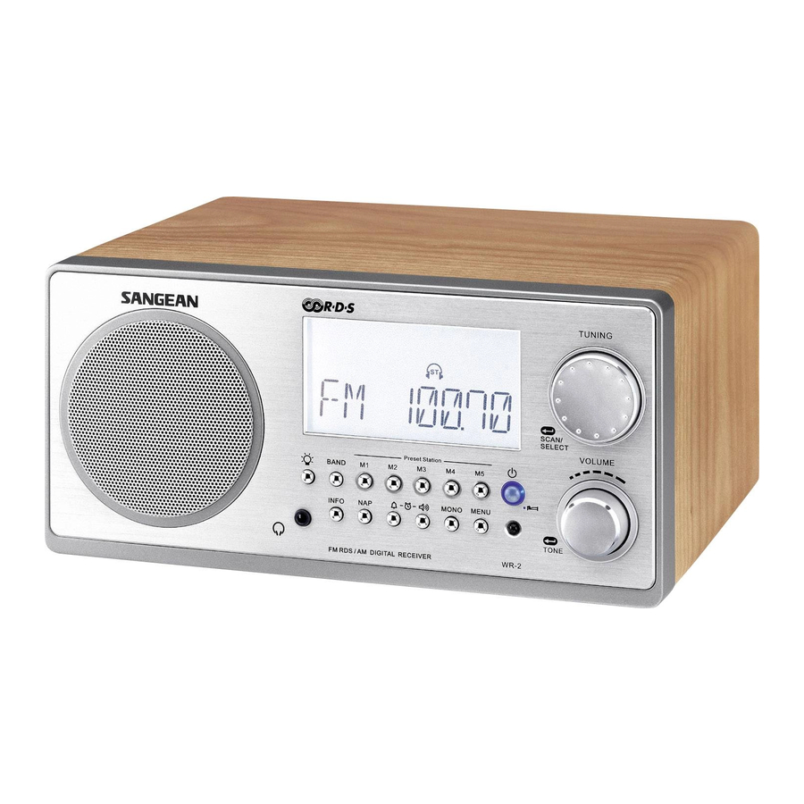
Sangean WR-2 Service Manual
Fm rds/am pll synthesized receiver
Hide thumbs
Also See for WR-2:
- Operating instructions manual (125 pages) ,
- Service manual (44 pages) ,
- Instruction manual (31 pages)
Table of Contents
Advertisement
FM RDS/AM PLL SYNTHESIZED
Specification .....................................................................................................................2-8
Block Diagram .....................................................................................................................9
Alignment Instructions.........................................................................................................10-15
Test Points Diagram.................................................................................................................16
Main PCB Top View.................................................................................................................17
Main PCB Bottom View..............................................................................................................18
Control PCB Top View..............................................................................................................19
Control PCB Bottom View.........................................................................................................20
Wiring Diagram............................................................................................................21
Troubleshooting Flow Chart.....................................................................................................22
Electrical Parts List.............................................................................................................23-26
Mechanical Parts List.........................................................................................................27-28
Exploded Views........................................................................................................................29
IC Circuit Block Diagram......................................................................................................30-37
IC and Transistor Voltage Chart..............................................................................................38-41
Semiconductor Lead Identifications...........................................................................................42
Main Schematic Diagram..........................................................................................................43
Control Schematic Diagram.......................................................................................................44
WR-2
RECEIVER
CONTENTS
Advertisement
Table of Contents

Related Manuals for Sangean WR-2


Summary of Contents for Sangean WR-2
-
Page 1: Table Of Contents
WR-2 FM RDS/AM PLL SYNTHESIZED RECEIVER CONTENTS Specification ………………………………………………………………………………………………………2-8 Block Diagram ………………………………………………………………………………………………………9 Alignment Instructions……………………………………………………………………………………………10-15 Test Points Diagram…………………………………………………………………………….……….……………16 Main PCB Top View…………………………………………………………………………….……….……………17 Main PCB Bottom View.………………………………………………………………………….……..………..…..18 Control PCB Top View……………………………………………………………………………….………….……19 Control PCB Bottom View……………………………………………………………………………………………20 Wiring Diagram..….………………………………………….………………….….……………..……….21 Troubleshooting Flow Chart..….………………………………………….……………….….……………..……22 Electrical Parts List………………………………………………………………………………..……………23-26 Mechanical Parts List………………………………………………………………….………….…………….27-28... -
Page 2: Specification
SPECIFICATION FM. ELECTRICAL PERFORMANCE Temp: 25 ℃ Model: WR-2(CE) Brand: SANGEAN R. H. : 75 % Date:2005/5/20 Condition Value Test No. Test Item Unit Input Output freq Nom. Lim. ±0.1 87.5 S/N=6dB Tuning Range ±0.1 S/N=6dB ±0.1 Intermediate freq. 10.7 S/N=6dB Max. - Page 3 SPECIFICATION FM. ELECTRICAL PERFORMANCE Temp: 25 ℃ Model: WR-2(USA) Brand: SANGEAN R. H. : 75 % Date: 2005/5/20 Condition Value Test No. Test Item Unit Input Output freq Nom. Lim. ±0.1 87.5 S/N=6dB Tuning Range ±0.1 S/N=6dB ±0.1 Intermediate freq.
- Page 4 SPECIFICATION MW ELECTRICAL PERFORMANCE Temp: 25 ℃ Model: WR-2(CE) Brand: SANGEAN R. H. : 75 % Date:2005/5/20 Condition Value Test No. Test Item Unit Input Output Freq. Nom. Lim. ±1 Min. S/N=6dB Tuning Range ±1 Max. 1629 S/N=6dB ±1 Intermediate freq.
- Page 5 SPECIFICATION MW ELECTRICAL PERFORMANCE Temp: 25 ℃ Model: WR-2(UK) Brand: SANGEAN R. H. : 75 % Date:2005/5/20 Condition Value Test No. Test Item Unit Input Output Freq. Nom. Lim. ±1 Min. S/N=6dB Tuning Range ±1 Max. 1629 S/N=6dB ±1 Intermediate freq.
- Page 6 SPECIFICATION AUX-IN ELECTRICAL PERFORMANCE Temp: 25 ℃ Model: WR-2(ALL) Brand: ALL R. H. : 75 % Date: 2005/3/30 Condition Value Test No. Test Item Unit Input Output Freq. Nom. Lim. AUX IN=0.5V/100Hz Output Power THD=10% Output=R.0 (ATT=0) AUX IN Vrms...
- Page 7 SPECIFICATION MW ELECTRICAL PERFORMANCE Temp: 25 ℃ Model: WR-2(USA) Brand: SANGEAN R. H. : 75 % Date: 2005/5/20 Condition Value Test No. Test Item Unit Input Output Freq. Nom. Lim. ±1 Min. S/N=6dB Tuning Range ±1 Max. 1710 S/N=6dB ±1 Intermediate freq.
- Page 8 SPECIFICATION LW ELECTRICAL PERFORMANCE Temp: 25 ℃ Model: WR-2(UK) Brand: ROBERTS R. H. : 75 % Date:2005/3/14 Condition Value Test No. Test Item Unit Input Output Freq. Nom. Lim. ±3 Min. S/N=6dB Tuning Range ±3 Max. S/N=6dB ±3 Intermediate freq.
-
Page 9: Block Diagram
BLOCK DIAGRAM... -
Page 10: Alignment Instructions
ALIGNMENT INSTRUCTIONS 1. ALIGNMENT FOR AM/LW IF Required Instruments: AM IF Sweep Generator with scope Alignment Procedure Mode Adjustment Procedure (1) Press the power button to turn on the radio. (2) Connect the input terminal of AM IF sweep generator in series with a resistor of 1.2k ohm to the TP3 and TP4. - Page 11 2. ALIGNMENT FOR AM/LW TUNING VOLTAGE RANGE Required Instruments: Alignment Procedure Mode Adjustment Procedure (1) Turn on the radio. (2) Connect the probe of DVM to the test point TP29 and TP4. (3) Tune the AM frequency to 522 kHz. (4) Adjust L5 to have a reading of 1.2V ±0.04V.
- Page 12 3. ALIGNMENT FOR FM TUNING VOLTAGE Required Instruments Alignment Procedure Mode Adjustment Procedure (1) Turn on the radio. (2) Connect the probe of DVM to the TP29 and TP4. (3) Tune the FM frequency to 108MHz. (4) Adjust L1 to have a reading of 7.2V ±0.3V. Instrument Connection TP29...
- Page 13 WR-2L 4. ALIGNMENT FOR AM/LW SENSITIVITY Required Instruments AM Signal Generator SSVM Alignment Procedure Mode Adjustment Procedure (1) Turn on the radio. (2) Connect a SSVM to the speaker TP7 and TP8 terminals. (3) Connect an AM signal generator together with standard loop dummy antenna and feed 30% modulated signal to the AM ferrite bar antenna L2.
- Page 14 WR-2 4-1. ALIGNMENT FOR AM SENSITIVITY Required Instruments AM Signal Generator SSVM Alignment Procedure Mode Adjustment Procedure (1) Turn on the radio. (2) Connect a SSVM to the speaker TP7 and TP8 terminals. (3) Connect an AM signal generator together with standard loop dummy antenna and feed 30% modulated signal to the AM ferrite bar antenna L2.
- Page 15 5. ALIGNMENT FOR FM TUNING SENSITIVITY Required Instruments FM Signal Generator SSVM Alignment Procedure Mode Adjustment Procedure (1) Turn on radio. (2) Connect a SSVM to speaker TP7 and TP8. (3) Connect a FM signal generator to TP1 and TP2. (4) Set the signal generator to 22.5 kHz deviation with 1 kHz modulation.
-
Page 16: Test Points Diagram
TEST POINTS DIAGRAM... -
Page 17: Main Pcb Top View
MAIN PCB TOP VIEW... -
Page 18: Main Pcb Bottom View
MAIN PCB BOTTOM VIEW... -
Page 19: Control Pcb Top View
CONTROL PCB TOP VIEW... -
Page 20: Control Pcb Bottom View
CONTROL PCB BOTTOM VIEW... -
Page 21: Wiring Diagram
WIRING DIAGRAM... -
Page 22: Troubleshooting Flow Chart
TROUBLESHOOTING FLOW CHART ( 1 ) Weak sensitivity on FM mode Check whether the sensitivity is recovered if antenna is directly Check the antenna terminal and connected to the point between antenna circuit. C22 and C34. Check IF waveform. Check CF2, CF3, T2. ( 2 ) Weak sensitivity in AM band Check the antenna circuit and Is the reception in MW band O.K.? -
Page 23: Electrical Parts List
TOROID COIL 0.6mH L 300, 1210271 TC 10P 4.5mm WHT TC 3,4, 1210281 TC 20P 4.5mm RED TC 1, 1600661 LCD WR-2 SZ5307-TG-E LCD200, 1613001 PCB A WR-2 1613010 PCB C WR-2 1613120 PCB D WR-2 1620732 SP.3" 8Ω 7W 1631520 SLIDE SW.1P2C... - Page 24 ELECTRICAL PARTS LIST WR-2 PART NO DESCRIPTION Q'TY REMARK 1646040 AC SOCKET HJC-037P JK 300, 1647110 JACK DC HTJ-020-04AZ JK 2, 1650290 X'TAL 4.332MHz X 200, 1650530 X'TAL 75K +10 -20PPM 2x6 X 201, 1660341-A FILTER PFWLF450KS2A-A0 CF 1, 1664150-A...
- Page 25 ELECTRICAL PARTS LIST WR-2 PART NO DESCRIPTION Q'TY REMARK 5012261 CH CC 122K 50V X7R-C C 51,52, 5012361 CH CC 123K 50V X7R-C C 97,98, 5018001 CH CC 180J 50V NPO-C C 14, 5022001 CH CC 220J 50V NPO-C C 27,33,...
-
Page 26: Electrical Parts List
ELECTRICAL PARTS LIST WR-2 PART NO DESCRIPTION Q'TY REMARK 6100164 CH RD 1/16W 220KJ-C R 42,107,278,279, 6100165 CH RD 1/16W 270KJ-C R 268, 6100172 CH RD 1/16W 1MJ-C R 240, 6100184 CH RD 1/16W 10MJ-C R 108,110,111, 6100194 CH RD 1/16W OJ-C... -
Page 27: Mechanical Parts List
MECHANICAL PARTS LIST WR-2 Ref no PART NO. DESCRIPTION Q'TY DWG NO. REMARK 20K6040 PHONE JACK HOLDER A3-WR1-25A 20M7000 LCD LIGHT LENS A4-WR2-12A 20M7010 IR HOLDER A4-WR2-16A 20M7020 LENS HOLDER A3-WR2-17A 20M7030 BAR ANT HOLDER A3-WR2-18A 20M7040 BOSS HOLDER A3-WR2-19A... - Page 28 MECHANICAL PARTS LIST WR-2 Ref no PART NO. DESCRIPTION Q'TY DWG NO. REMARK 9102122 SCREW PTP 2.6x12(NI) PHONE JACK PCBx2 9103102 SCREW PTP 3X10(NI) AC JACKx2 9153082 SCREW PTPW 3x8(NI) TRANSx2 9163082 SCREW PTB 3.0x8(NI) SPEAKERx4/C PCBx4 BOSS HOLDERx2 9163142...
-
Page 30: Ic Circuit Block Diagram
IC CIRCUIT BLOCK DIAGRAM IC1 – LA1177 IC2 – TA2099F... - Page 31 IC3 – BA09T IC4 – TDA7313D...
- Page 32 IC5 – TDA7266L IC6 – TC7S66FU...
- Page 33 IC7 – NJM4580D IC8 – PT2308...
- Page 34 IC200 – H7805AM 10. IC201 – XC62AP4002...
- Page 35 11. IC202 – TC9324F...
- Page 36 12. IC203 – BU1924F 13. IC204 – XC61CN2002MR...
- Page 37 14. IC205 – XC61CN3502MR...
-
Page 38: Ic And Transistor Voltage Chart
IC AND TRANSISTOR VOLTAGE CHART IC1 – LA1177 IC2 – TA2099F IC3 – BA09T IC4 – TDA7313D 11.17 9.08 IC5 – TDA7266L IC6 – TC7S66FU IC7 – NJM4580D IC8 – PT2308 IC200 – H7805AM IC201 – XC62AP4002... - Page 39 IC202 – TC9324F PIN FM MW LW AUX OFF PIN FM MW LW AUX OFF PIN FM MW LW AUX OFF 100 2.0...
- Page 40 IC203 – BU1924F IC204 – XC61CN2002MR IR200 – PNA4312M 2.16 2.13 2.15 4.31 2.13...
- Page 41 Transistor Q208 5.06 4.22 Q209 7.88 Q204 0.18 3.46 Q205 2.62 Q200 Q203 Q201 Q206 Q202 Q207 Q207...
-
Page 42: Semiconductor Lead Identifications
SEMICONDUCTOR LEAD IDENTIFICATIONS Transistors 3SK263 2SA812 2SK433B UNR5110 2SB1295 UNR5113 2SC1623 UNR5210 2SC4081 UNR5211 2SC4154 (E:Emitter C:Collector B:Base) Diodes 1SS367 FR204 1SS314 BAV99 WAP200U SVC220 SVC383 (A:Anode C:Cathode) -
Page 43: Main Schematic Diagram
MAIN SCHEMATIC DIAGRAM... -
Page 44: Control Schematic Diagram
CONTROL SCHEMATIC DIAGRAM...
Need help?
Do you have a question about the WR-2 and is the answer not in the manual?
Questions and answers