Advertisement
FM TRANSCEIVER
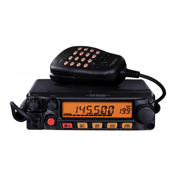
FT-1900R
Technical Supplement
©2009 VERTEX STANDARD CO., LTD.
Introduction
This manual provides technical information necessary for servicing the FT-1900R FM Transceiver.
Servicing this equipment requires expertise in handling surface-mount chip components. Attempts by non-
qualified persons to service this equipment may result in permanent damage not covered by the warranty,
and may be illegal in some countries.
Two PCB layout diagrams are provided for each double-sided circuit board in the Transceiver. Each side of
is referred to by the type of the majority of components installed on that side ("leaded" or "chip-only"). In
most cases one side has only chip components, and the other has either a mixture of both chip and leaded
components (trimmers, coils, electrolytic capacitors, ICs, etc.), or leaded components only.
While we believe the technical information in this manual to be correct, VERTEX STANDARD assumes no
liability for damage that may occur as a result of typographical or other errors that may be present. Your
cooperation in pointing out any inconsistencies in the technical information would be appreciated.
The transceiver was assembled using Pb (lead) free solder, based on the RoHS specification.
Only lead-free solder (Alloy Composition: Sn-3.0Ag-0.5Cu) should be used for repairs performed on this appara-
tus. The solder stated above utilizes the alloy composition required for compliance with the lead-free specification,
and any solder with the above alloy composition may be used.
Specifications ...................................................... 2
Exploded View & Miscellaneous Parts ............ 3
Block Diagram .................................................... 5
Connection Diagram .......................................... 6
Circuit Description ............................................. 7
Alignment ............................................................ 9
VERTEX STANDARD CO., LTD.
4-8-8 Nakameguro, Meguro-Ku, Tokyo 153-8644, Japan
VERTEX STANDARD
US Headquarters
10900 Walker Street, Cypress, CA 90630, U.S.A.
YAESU UK LTD.
Unit 12, Sun Valley Business Park, Winnall Close
Winchester, Hampshire, SO23 0LB, U.K.
VERTEX STANDARD HK LTD.
Unit 5, 20/F., Seaview Centre, 139-141 Hoi Bun Road,
Kwun Tong, Kowloon, Hong Kong
VERTEX STANDARD ( AUSTRALIA ) PTY., LTD.
Normanby Business Park, Unit 14/45 Normanby Road
EH023N91A
Notting Hill 3168, Victoria, Australia
Important Note
Contents
Board Unit
MAIN Unit Circuit Diagram ................................. 13
MAIN Unit Parts Layout ...................................... 15
MAIN Unit Parts List ............................................ 17
CNTL Unit Circuit Diagram .................................. 27
CNTL Parts Layout ............................................... 28
CNTL Parts List .................................................... 29
(Schematics, Layouts & Parts)
1
Advertisement
Table of Contents

Related Manuals for Yaesu FT-1900R


Summary of Contents for Yaesu FT-1900R
-
Page 1: Table Of Contents
Notting Hill 3168, Victoria, Australia Introduction This manual provides technical information necessary for servicing the FT-1900R FM Transceiver. Servicing this equipment requires expertise in handling surface-mount chip components. Attempts by non- qualified persons to service this equipment may result in permanent damage not covered by the warranty, and may be illegal in some countries. -
Page 2: Specifications
Specifications General Frequency Range: Tx 144 - 146 MHz or 144 - 148 MHz Rx 144 - 146 MHz or 136 - 174 MHz Channel Step: 5/10/12.5/15/20/25/50/100 kHz Standard Repeater Shift: ±600 kHz Frequency Stability: Better than ±10 ppm [–4 °F to +140 °F (–20 °C to +60 °C)] Modes of Emission: F2D/F3E Antenna Impedance:... -
Page 3: Exploded View & Miscellaneous Parts
DC CABLE ( FT-1900R ) T9021715 T9207482 RA60H1317M1 DC CABLE ( FT-1900E ) WIRE ASSY T9022815 SPARE FUSE ( 15 A: FT-1900R ) Q0000151 SPARE FUSE ( 15 A: FT-1900E ) Q0000075 BRACKET ( MMB-36 ) D6000055 CB0297000 SCREW SET REF. - Page 4 Note...
-
Page 5: Block Diagram
Block Diagram... -
Page 6: Connection Diagram
Connection Diagram... -
Page 7: Circuit Description
Circuit Description Receive Signal Path The audio signal passes through a band-pass filter consisting of Q1046 and Q1047 (both 2SC4154), and Incoming RF signal is from the antenna jack is de- the audio mute gate Q1039 (2SJ347), to the audio livered to the Main Unit and passed through the low- VR which adjusts the audio sensitivity to compen- pass filter network consisting capacitors C1213,... - Page 8 Circuit Description TX APC Circuit to the frequency dividing data that is associated with the setting frequency input from the main CPU A portion of the power amplifier module output is Q2002 (HD64F2266TF13). It is then sent to the phase rectified by D1022 (1SS321), then delivered to APC c o m p a r a t o r s e c t i o n o f t h e P L L I C Q 1 0 1 1 Q1038 (LM2904PWR), as a DC voltage which is pro-...
-
Page 9: Alignment
Alignment Introduction Required Test Equipment The FT-1900R is carefully aligned at the factory for The following test equipment (and familiarity with the specified performance across the amateur band. its use) is necessary for complete realignment. Cor- Realignment should therefore not be necessary ex- rection of problems caused by misalignment result- cept in the event of a component failure. -
Page 10: Test Setup
B0111 tL B0111 tL.” rameter to “B0111 tL B0111 tL Alignment of the FT-1900R is performed using a Press the [ D/MR ( MW )] key to enable adjustment front panel software-based procedure. To perform of the “Squelch Threshold Level.”... - Page 11 Alignment S-meter Level (S-1) TX Power (Low 2) Rotate the DIAL knob to set the alignment pa- Inject a 145.100 MHz signal at a level of –5 dBµ rameter to “B0101 L2 B0101 L2 B0101 L2 B0101 L2 B0101 L2.” (with 1 kHz modulation @±3.5 kHz deviation) Press the [ D/MR ( MW )] key to enable adjustment from the RF signal generator.
- Page 12 Alignment Closing the Alignment mode DCS TX Deviation Rotate the DIAL knob to set the alignment pa- 1. Press the [DW(REV)] key to save the new setting and rameter to “B0101 dC B0101 dC B0101 dC B0101 dC B0101 dC.” exit to normal operation.
-
Page 13: Main Unit Circuit Diagram
MAIN Unit Circuit Diagram 4.3 V RX: 6.1 V RX: 0 V 4.1 V TX: 4.2 V RX: 0 V TX: 2.0 V TX: 5.0 V RX: 0 V RX: 0 V RX: 0.5 V TX: 6.9 V TX: 1.6 V TX: 0.6 V RX: 0 V 3.2 V... - Page 14 MAIN Unit Note...
-
Page 15: Main Unit Parts Layout
MAIN Unit Parts Layout (Side A) RA60H1317M1 KIA7808API LA4425A (Q1030) (Q1015) (Q1035) 2SA1774 (FR) 2SJ615 2SC4081 (B) (Q1007) (Q1008) (Q1033) 2SC4400 (RT4) (Q1032) 2SC4617 (BR) (Q1051, 1053) 2SC5226 (R22) (Q1026) 2SC5231 (C9) CD4094BPWR 3SK299 (U73) (Q1009) (Q1048) (Q1037, 1045) 2SC5374 (NA) MB15A01PFV1 (Q1010, 1017, 1023) (Q1011) - Page 16 MAIN Unit Parts Layout (Side B) LM2902PWR M62364FP LM2904PWR (Q1005, 1049) (Q1043) (Q1006, 1038, 1044, 1050) 2SA1774 (FR) 2SJ347 (KS) 2SJ364 (4M) (Q1024, 2027, 1029) (Q1039) (Q1034, 1036, 1041, 1042) 2SC4081 (B) DTC144EE (26) S-812C50AUA (Q1001, 1012, 1021, (Q1013, 1018, 1019, (Q1016) 1046, 1047) 1020, 1031, 1040)
-
Page 17: Main Unit Parts List
MAIN Unit Parts List DESCRIPTION VALUE TOL. MFR'S DESIG VXSTD P/N VERS. LOT SIDE LAY ADR PCB with Components CB3119006 CE:OFF, DST:USA2 CB3119007 CE:OFF, DST:EXP2 Printed Circuit Board AH023N000 FR013240E C 1001 CHIP TA.CAP. 10uF TAJA106M010Y K78100072 C 1002 CHIP TA.CAP. 10uF TAJA106M010Y K78100072... - Page 18 MAIN Unit Parts List DESCRIPTION VALUE TOL. MFR'S DESIG VXSTD P/N VERS. LOT SIDE LAY ADR C 1078 CHIP CAP. 0.015uF GRM188B11H153KA01D K22174838 C 1079 CHIP CAP. 150pF GRM1882C1H151JA01D K22174239 C 1080 CHIP CAP. 560pF GRM1882C1H561JA01D K22174273 C 1081 CHIP CAP. 0.001uF GRM188B11H102KA01D K22174821...
- Page 19 MAIN Unit Parts List DESCRIPTION VALUE TOL. MFR'S DESIG VXSTD P/N VERS. LOT SIDE LAY ADR C 1156 CHIP CAP. 0.001uF GRM188B11H102KA01D K22174821 C 1157 CHIP CAP. 0.01uF GRM188B11H103KA01D K22174823 C 1158 CHIP CAP. 0.001uF GRM188B11H102KA01D K22174821 C 1161 CHIP CAP. 0.047uF GRM188B11E473KA01D K22144811...
- Page 20 MAIN Unit Parts List DESCRIPTION VALUE TOL. MFR'S DESIG VXSTD P/N VERS. LOT SIDE LAY ADR C 1244 CHIP CAP. 0.001uF GRM188B11H102KA01D K22174821 C 1245 CHIP CAP. 10pF GRM1882C1H100JA01D K22174211 C 1248 CHIP CAP. 39pF GRM1882C1H390JA01D K22174225 C 1249 CHIP CAP. GRM1884C1H2R0CZ01D K22174203 C 1250...
- Page 21 MAIN Unit Parts List DESCRIPTION VALUE TOL. MFR'S DESIG VXSTD P/N VERS. LOT SIDE LAY ADR FB1007 FERRITE BEADS BK1608HS121-T L9190081 J 1001 CONNECTOR SC25-02WS P0090621 J 1002 CONNECTOR HSJ0836-0105009 P1091085 J 1003 CONNECTOR 32FLT-SM2-TB(LF)(SN)(M) P1091258 L 1002 CHIP COIL 0.056uH LQW2BHN56NG03L L1690978...
- Page 22 MAIN Unit Parts List DESCRIPTION VALUE TOL. MFR'S DESIG VXSTD P/N VERS. LOT SIDE LAY ADR Q 1051 TRANSISTOR 2SC4617 TL R G3346178R Q 1052 TRANSISTOR DTC143EE TL G3070114 Q 1053 TRANSISTOR 2SC4617 TL R G3346178R R 1001 CHIP RES. 3.3k 1/16W RMC1/16S 332JTH...
- Page 23 MAIN Unit Parts List DESCRIPTION VALUE TOL. MFR'S DESIG VXSTD P/N VERS. LOT SIDE LAY ADR R 1076 CHIP RES. 390k 1/16W RMC1/16S 394JTH J24189056 R 1077 CHIP RES. 1/16W RMC1/16S 223JTH J24189041 R 1079 CHIP RES. 2.2k 1/16W RMC1/16S 222JTH J24189029 R 1081 CHIP RES.
- Page 24 MAIN Unit Parts List DESCRIPTION VALUE TOL. MFR'S DESIG VXSTD P/N VERS. LOT SIDE LAY ADR R 1156 CHIP RES. 1/16W RMC1/16S 393JTH J24189044 R 1157 CHIP RES. 330k 1/16W RMC1/16S 334JTH J24189055 R 1158 CHIP RES. 330k 1/16W RMC1/16S 334JTH J24189055 R 1159 CHIP RES.
- Page 25 MAIN Unit Parts List DESCRIPTION VALUE TOL. MFR'S DESIG VXSTD P/N VERS. LOT SIDE LAY ADR R 1236 CHIP RES. 2.2k 1/16W RMC1/16S 222JTH J24189029 R 1237 CHIP RES. 1/16W RMC1/16S 681JTH J24189023 R 1238 CHIP RES. 4.7k 1/16W RMC1/16S 472JTH J24189033 R 1239 CHIP RES.
- Page 26 MAIN Unit Note...
-
Page 27: Cntl Unit Circuit Diagram
CNTL Unit Circuit Diagram 8.0 V 5.0 V 3.4 V 2.3 V 2.6 V 2.6 V 5.0 V 5.0 V RX: 4.8 V TX: 0.6 V RX: 4.8 V TX: 0.6 V 3.9 V 5.0 V 5.0 V 2.5 V 4.8 V 5.0 V 1.8 V... -
Page 28: Cntl Parts Layout
CNTL Unit Parts Layout (Side A) CPH6202 (CB) DTC143ZE (E23) (Q2005) (Q2004) (Side A) 2SC4617 (BR) BD4830FVE (Q2007, 2008, 2013) (Q2011) 2SC5374 (NA) (Q2003) S-812C50AUA DTC143ZE (E23) (Q2010) (Q2012) (Side B) DA221 (26) DAN222 (N) (D2001, 2025) (D2023) HD64F2266TF13 BR24L64 (Q2002) (Q2006) -
Page 29: Cntl Parts List
CNTL Unit Parts List DESCRIPTION VALUE TOL. MFR'S DESIG VXSTD P/N VERS. LOT SIDE LAY ADR PCB with Components CS2033409 CE:OFF, DST:USA2, TYP:A2 CS2033410 CE:OFF, DST:EXP2, TYP:A1 CS2033411 CE:OFF, DST:EXP2, TYP:A2 CS2033412 CE:OFF, DST:EXP2, TYP:A3 CS2033415 CE:OFF, DST:EXP2, TYP:B3 Printed Circuit Board FR013250D C 2001 CHIP CAP. - Page 30 CNTL Unit Parts List DESCRIPTION VALUE TOL. MFR'S DESIG VXSTD P/N VERS. LOT SIDE LAY ADR D 2009 SML-512WWT86 G2071104 D 2010 SML-512WWT86 G2071104 D 2011 DIODE 1SS400 TE61 G2070634 D 2012 DIODE 1SS400 TE61 G2070634 D 2013 SML-512WWT86 G2071104 D 2014 SML-512WWT86 G2071104...
- Page 31 CNTL Unit Parts List DESCRIPTION VALUE TOL. MFR'S DESIG VXSTD P/N VERS. LOT … LAY ADR R 2039 CHIP RES. 1/16W RMC1/16S 683JTH J24189047 R 2040 CHIP RES. 220k 1/16W RMC1/16S 224JTH J24189053 R 2041 CHIP RES. 6.8k 1/16W RMC1/16S 682JTH J24189035 R 2042 CHIP RES.
- Page 32 CNTL Unit Note...
- Page 34 Copyright 2009 VERTEX STANDARD CO., LTD. All rights reserved No portion of this manual may be reproduced without the permission of VERTEX STANDARD CO., LTD. Printed in Japan.
Need help?
Do you have a question about the FT-1900R and is the answer not in the manual?
Questions and answers