Samsung VP-M50 Service Manual
8mm
Hide thumbs
Also See for VP-M50:
- Owner's instruction book (63 pages) ,
- Owner's instruction manual (62 pages)
Table of Contents
Advertisement
© Samsung Electronics Co.,Ltd. MAR. 2000
Printed in Korea
AD68-00079N
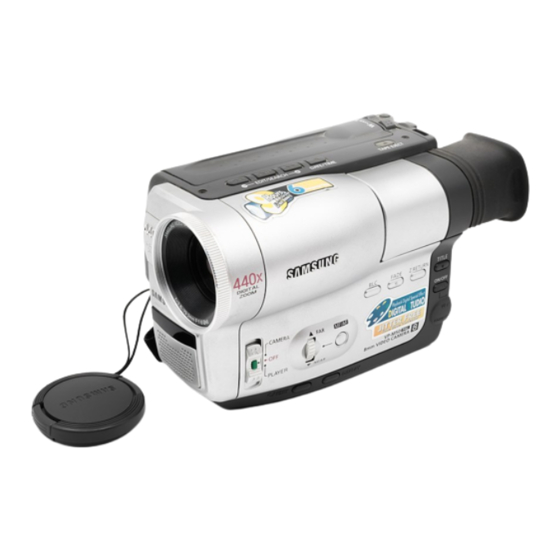
8mm CAMCORDER
VP-M50/SCM50
VP-M51/SCM51
VP-M52/SCM52
VP-M53/SCM53
VP-M54
VP-M51B
SERVICE
For mechanical disassembly and adjustment, refer to the "Mechanical Manual"
(DE-6
AD68-30200A).
8mm CAMCORDER
Manual
CONTENTS
1. Precautions
2. Product Specifications and
Comparison Chart
3. Disassembly and Reassembly
4. Alignment and Adjustment
5. Exploded View and Parts List
6. Electrical Parts List
7. PCB Diagrams
8. Wiring Diagram
9. Schematic Diagrams
Advertisement
Table of Contents

Related Manuals for Samsung VP-M50


Summary of Contents for Samsung VP-M50
- Page 1 2. Product Specifications and Comparison Chart 3. Disassembly and Reassembly 4. Alignment and Adjustment 5. Exploded View and Parts List 6. Electrical Parts List 7. PCB Diagrams 8. Wiring Diagram 9. Schematic Diagrams © Samsung Electronics Co.,Ltd. MAR. 2000 Printed in Korea AD68-00079N...
-
Page 2: Precautions
Alternatively, wear a dis- tion, replace the picture tube only with one that is the same type as the original. charging Wrist-strap device. (Be sure to remove it prior to applying power--this is an electric shock precaution.) Samsung Electronics... - Page 3 17. Observe the original lead dress, especially near the following areas : Antenna wiring, sharp edges, and especially the AC and high voltage power supplies. Always inspect for pinched, out-of-place, or frayed wiring. Do not change the spacing between components and the Samsung Electronics...
-
Page 4: Product Specifications And
SCM50/M51/M52: 3.9W, SCM53: 4.4W Built-in mic Condenser mic, omni-directional Operating temperature 0°C to 40°C (32°F to 104°F) Dimension (W x H x D) 101 x 104 x 174.3 (mm) ; 39.7 x 40.9 x 68.6 (inch) Weight 670g (1/49 lbs) Samsung Electronics... -
Page 5: Disassembly And Reassembly
3. Disassembly and Reassembly 3-1. Cabinet and PCB 3-1-1 Ass’y Cover Housing Removal REMOVE 2 SCREWS. "A" Remove the ass'y cover housing in the direction of arrow Fig. 3-1 Ass’y Cover Housing Removal Samsung Electronics... - Page 6 REASSEMBLY : PUT THE 4 TABS INTO THE SLOT, WHILE SLIDING IT AS SHOWN IN DETAIL "B". 1 LOCKING TAB "B" PRECISION SCREW DRIVER < DETAIL "B" > < DETAIL "A" > Fig. 4-2 Ass’y Case Top Removal Samsung Electronics...
-
Page 7: Alignment And Adjustment
PB RF - Pin 11 of CN452 Head Switching Trigger - Pin 9 of CN452 CN452 CN452 PB RF Head Switching - Trigger SW471 J451 DC-JACK Fig. 1 Test point Fig. 2 Test location of test point (Rear Board) Samsung Electronics... - Page 8 The camera will move both zoom and focus lens. The adjustment is finished when the O.K! message appears on the TV screen. Store the data to mode 0A6, 0A7, 0A8, 0A9, 0AA, 0AB, 0AC or 0AD. (3M±1cm) (Be sure to maintain the distance.) LENS 4-22 Samsung Electronics...
-
Page 9: Exploded View And Parts List
5-7 Mechanical Parts (2) - - - - - - - - - - - - - - - - - - - - -5-14 5-8 Mechanical Parts (3) - - - - - - - - - - - - - - - - - - - - -5-16 Samsung Electronics... -
Page 10: Electrical Parts List
2203-000626 C-CERAMIC,CHIP;0.022nF,5%,50V,NP0,TP,160 C053 2203-001686 C-CERAMIC,CHIP;0.075nF,5%,50V,NP0,TP,160 C121 2203-000257 C-CERAMIC,CHIP;10nF,10%,50V,X7R,TP,1608 C054 2203-000357 C-CERAMIC,CHIP;0.15nF,5%,50V,NP0,TP,1608 C122 2203-000189 C-CERAMIC,CHIP;100nF,+80-20%,25V,Y5V,TP, C055 2203-000236 C-CERAMIC,CHIP;0.1nF,5%,50V,NP0,TP,1608 C123 2203-001195 C-CERAMIC,CHIP;0.007nF,0.25pF,50V,NP0,TP C056 2203-000189 C-CERAMIC,CHIP;100nF,+80-20%,25V,Y5V,TP, C124 2203-002605 C-CERAMIC,CHIP;0.008nF,0.25pF,50V,NP0,TP C061 2203-001408 C-CERAMIC,CHIP;0.27nF,5%,50V,NP0,TP,1608 C125 2203-000426 C-CERAMIC,CHIP;0.018nF,5%,50V,NP0,TP,160 C101 2203-000257 C-CERAMIC,CHIP;10nF,10%,50V,X7R,TP,1608 C126 2203-000384 C-CERAMIC,CHIP;0.015nF,5%,50V,NP0,TP,160 Samsung Electronics... - Page 11 7-9 Function PCB - - - - - - - - - - - - - - - - - - - - - - - - - - 7-14 7-10 Front PCB - - - - - - - - - - - - - - - - - - - - - - - - - - - - 7-15 Samsung Electronics...
- Page 12 8. Wiring Diagram Samsung Electronics...
-
Page 13: Table Of Contents
9-11 Function - - - - - - - - - - - - - - - - - - - - - - - - - - - - - 9-14 9-12 EVF - - - - - - - - - - - - - - - - - - - - - - - - - - - - - - - - - 9-15 Samsung Electronics... - Page 14 Schematic Diagrams OPTION LIST VALUE(BASIC) SCM50 SCM51 SCM52 SCM53 VP-M50 VP-M51 VP-M51(B) VP-M52 VP-M53 VP-M54 OPTION VALUE(BASIC) SCM50 SCM51 SCM52 SCM53 VP-M50 VP-M51 VP-M51(B) VP-M52 VP-M53 VP-M54 OPTION C156 120,50V,* NTSC CW02 10/10V, XDR O 150,50V,* CW03 104,25V,* XDR O...
- Page 15 Schematic Diagrams VALUE(BASIC) SCM50 SCM51 SCM52 SCM53 VP-M50 VP-M51 VP-M51(B) VP-M52 VP-M53 VP-M54 OPTION VALUE(BASIC) SCM50 SCM51 SCM52 SCM53 VP-M50 VP-M51 VP-M51(B) VP-M52 VP-M53 VP-M54 OPTION R235 000,(1/16W),* None RD51 10,1/16W,* DIS O R241 1K,(1/16W),* None RP100 000,(1/16W),* B&W R247 4.7K,(1/16W),*...
-
Page 16: Dc/Dc Converter (Main)
Schematic Diagrams 9-1 DC/DC Converter (Main) Samsung Electronics... -
Page 17: System Control/Servo (Main)
Schematic Diagrams 9-2 System Control/Servo (Main) Samsung Electronics... -
Page 18: Video (Normal) (Main)
Schematic Diagrams 9-3 Video (Normal) (Main) Samsung Electronics... -
Page 19: Video (Hi8) (Main)
Schematic Diagrams 9-4 Video (Hi8) (Main) Samsung Electronics... -
Page 20: Audio (Main)
Schematic Diagrams 9-5 Audio (Main) Samsung Electronics... -
Page 21: Camera (Main)
Schematic Diagrams 9-6 Camera (Main) Samsung Electronics... -
Page 22: Rear
Schematic Diagrams 9-7 Rear 9-10 Samsung Electronics... -
Page 23: Ccd
Schematic Diagrams 9-8 CCD Samsung Electronics 9-11... -
Page 24: Cvf
Schematic Diagrams 9-9 CVF 9-12 Samsung Electronics... -
Page 25: Front
Schematic Diagrams 9-10 Front Samsung Electronics 9-13... -
Page 26: Function
Schematic Diagrams 9-11 Function 9-14 Samsung Electronics... -
Page 27: Evf
Schematic Diagrams 9-12 EVF Samsung Electronics 9-15... -
Page 28: Samsung Electronics
Wiring Diagram MEMO MEMO Samsung Electronics... -
Page 29: Pcb Diagrams
PCB Diagrams 7-1 Main PCB (Normal) (Component Side) Samsung Electronics... - Page 30 PCB Diagrams Samsung Electronics...
- Page 31 PCB Diagrams 7-2 Main PCB (Normal) (Conductor Side) Samsung Electronics...
- Page 32 PCB Diagrams Samsung Electronics...
- Page 33 PCB Diagrams 7-3 Main PCB (Hi8) (Component Side) Samsung Electronics...
- Page 34 PCB Diagrams Samsung Electronics...
- Page 35 PCB Diagrams 7-4 Main PCB (Hi8) (Conductor Side) Samsung Electronics...
- Page 36 PCB Diagrams Samsung Electronics...
- Page 37 PCB Diagrams 7-5 Rear PCB (VP-M54 only) (Component Side) (Conductor Side) 7-10 Samsung Electronics...
- Page 38 PCB Diagrams 7-6 CCD PCB (Component Side) (Conductor Side) Samsung Electronics 7-11...
- Page 39 PCB Diagrams 7-7 CVF PCB (Component Side) (Conductor Side) 7-12 Samsung Electronics...
- Page 40 PCB Diagrams 7-8 EVF PCB (Component Side) (Conductor Side) Samsung Electronics 7-13...
- Page 41 PCB Diagrams 7-9 Function PCB (Component Side) (Conductor Side) 7-14 Samsung Electronics...
- Page 42 PCB Diagrams 7-10 Front PCB Samsung Electronics 7-15...
- Page 43 PCB Diagrams MEMO MEMO 7-16 Samsung Electronics...
- Page 44 2203-000257 C-CERAMIC,CHIP;10nF,10%,50V,X7R,TP,1608 C153 2203-000604 C-CERAMIC,CHIP;22nF,10%,25V,X7R,TP,1608 C224 2203-000715 C-CERAMIC,CHIP;3.3nF,10%,50V,X7R,TP,1608 C154 2203-000257 C-CERAMIC,CHIP;10nF,10%,50V,X7R,TP,1608 C224 2203-001652 C-CERAMIC,CHIP;470nF,+80-20%,16V,Y5V,TP, C154 2203-000332 C-CERAMIC,CHIP;0.012nF,5%,50V,NP0,TP,160 C225 2203-000189 C-CERAMIC,CHIP;100nF,+80-20%,25V,Y5V,TP, C155 2203-000257 C-CERAMIC,CHIP;10nF,10%,50V,X7R,TP,1608 C225 2404-001131 C-TA,CHIP;22UF,10%,10V,GP,TP,3528 C155 2203-000604 C-CERAMIC,CHIP;22nF,10%,25V,X7R,TP,1608 C226 2203-000189 C-CERAMIC,CHIP;100nF,+80-20%,25V,Y5V,TP, C156 2203-000384 C-CERAMIC,CHIP;0.015nF,5%,50V,NP0,TP,160 C226 2203-001640 C-CERAMIC,CHIP;0.39nF,10%,50V,X7R,TP,160 Samsung Electronics...
- Page 45 2203-001607 C-CERAMIC,CHIP;0.22nF,5%,50V,NP0,TP,1608 C539 2203-000189 C-CERAMIC,CHIP;100nF,+80-20%,25V,Y5V,TP, C720 2203-000189 C-CERAMIC,CHIP;100nF,+80-20%,25V,Y5V,TP, C541 2404-000284 C-TA,CHIP;10uF,20%,16V,-,TP,3528,- C721 2203-000189 C-CERAMIC,CHIP;100nF,+80-20%,25V,Y5V,TP, C542 2203-001640 C-CERAMIC,CHIP;0.39nF,10%,50V,X7R,TP,160 C722 2203-000491 C-CERAMIC,CHIP;2.2nF,10%,50V,X7R,TP,1608 C543 2203-001662 C-CERAMIC,CHIP;5.6nF,10%,50V,NP0,TP,1608 C723 2404-000151 C-TA,CHIP;1uF,20%,16V,-,TP,3216,- C544 2203-000888 C-CERAMIC,CHIP;4.7nF,10%,50V,X7R,TP,1608 C728 2404-000151 C-TA,CHIP;1uF,20%,16V,-,TP,3216,- C545 2203-001103 C-CERAMIC,CHIP;6.8nF,10%,50V,X7R,TP,1608 C729 2404-001020 C-TA,CHIP;10uF,20%,10V,GP,TP,3216,3.2 Samsung Electronics...
- Page 46 0407-000139 DIODE-ARRAY;IMN10,80V,100mA,CX3,IMD,TP CP68 2203-000257 C-CERAMIC,CHIP;10nF,10%,50V,X7R,TP,1608 DP01 0405-000143 DIODE-VARACTOR;MA341,30V,10nA,MINI-2,TP CP69 2203-000998 C-CERAMIC,CHIP;0.047nF,5%,50V,NP0,TP,160 DP02 0401-001054 DIODE-SWITCHING;KDS160,85V,300mA,SOD-323 CP70 2203-000257 C-CERAMIC,CHIP;10nF,10%,50V,X7R,TP,1608 DP03 0407-000148 DIODE-ARRAY;MA141WK,40V,150mA,CA2-3,SC-7 CP71 2203-000681 C-CERAMIC,CHIP;0.027nF,5%,50V,NP0,TP,160 DP04 0401-001054 DIODE-SWITCHING;KDS160,85V,300mA,SOD-323 CP72 2203-000189 C-CERAMIC,CHIP;100nF,+80-20%,25V,Y5V,TP, DP05 0401-001054 DIODE-SWITCHING;KDS160,85V,300mA,SOD-323 CP73 2203-000189 C-CERAMIC,CHIP;100nF,+80-20%,25V,Y5V,TP, DP06 0401-001058 DIODE-SWITCHING;KDS121,85V,300mA,SOT-323 Samsung Electronics...
- Page 47 0501-002171 TR-SMALL SIGNAL;KTA2014,PNP,100mW,SOT-32 LP10 2703-001883 INDUCTOR-SMD;22uH,10%,2.5x2x1.8mm Q282 0506-000151 TR-ARRAY;UMZ1N,NPN/PNP,1,50V,40V,100mA, LP11 2703-001883 INDUCTOR-SMD;22uH,10%,2.5x2x1.8mm Q288 0504-001032 TR-DIGITAL;KRC404,NPN,100MW,47K/47K,SOT- LP12 2703-001883 INDUCTOR-SMD;22uH,10%,2.5x2x1.8mm Q301 0501-002128 TR-SMALL SIGNAL;KTC4075,NPN,100mW,USM,TP NOR Q001 0506-000146 TR-ARRAY;UMH6N,NPN,2,150mW,UM6,TP,68 Q302 0501-002128 TR-SMALL SIGNAL;KTC4075,NPN,100mW,USM,TP NOR Q004 0504-001032 TR-DIGITAL;KRC404,NPN,100MW,47K/47K,SOT- Q348 0501-002171 TR-SMALL SIGNAL;KTA2014,PNP,100mW,SOT-32 Samsung Electronics...
- Page 48 2007-000079 R-CHIP;1.8Kohm,5%,1/16W,DA,TP,1608 R133 2007-000121 R-CHIP;820ohm,5%,1/16W,DA,TP,1608 R165 2007-000123 R-CHIP;1.5Kohm,5%,1/16W,DA,TP,1608 R134 2007-000075 R-CHIP;220ohm,5%,1/16W,DA,TP,1608 R166 2007-000078 R-CHIP;1Kohm,5%,1/16W,DA,TP,1608 R134 2007-000078 R-CHIP;1Kohm,5%,1/16W,DA,TP,1608 R167 2007-000458 R-CHIP;18Kohm,5%,1/16W,DA,TP,1608 R135 2007-000081 R-CHIP;2.7Kohm,5%,1/16W,DA,TP,1608 R168 2007-000458 R-CHIP;18Kohm,5%,1/16W,DA,TP,1608 R135 2007-000643 R-CHIP;270ohm,5%,1/16W,DA,TP,1608 R169 2007-000078 R-CHIP;1Kohm,5%,1/16W,DA,TP,1608 R136 2007-000082 R-CHIP;3.3Kohm,5%,1/16W,DA,TP,1608 R170 2007-000123 R-CHIP;1.5Kohm,5%,1/16W,DA,TP,1608 6-10 Samsung Electronics...
- Page 49 2007-000503 R-CHIP;2.2ohm,5%,1/16W,DA,TP,1608 R392 2007-000078 R-CHIP;1Kohm,5%,1/16W,DA,TP,1608 R519 2007-000503 R-CHIP;2.2ohm,5%,1/16W,DA,TP,1608 R392 2007-000084 R-CHIP;4.7Kohm,5%,1/16W,DA,TP,1608 R520 2007-000503 R-CHIP;2.2ohm,5%,1/16W,DA,TP,1608 R393 2007-000078 R-CHIP;1Kohm,5%,1/16W,DA,TP,1608 R521 2007-000483 R-CHIP;1OHM,5%,1/10W,DA,TP,2012 R401 2007-000450 R-CHIP;180ohm,5%,1/16W,DA,TP,1608 R522 2007-000483 R-CHIP;1OHM,5%,1/10W,DA,TP,2012 R402 2007-000078 R-CHIP;1Kohm,5%,1/16W,DA,TP,1608 R523 2007-000483 R-CHIP;1OHM,5%,1/10W,DA,TP,2012 R403 2007-000078 R-CHIP;1Kohm,5%,1/16W,DA,TP,1608 R524 2007-000483 R-CHIP;1OHM,5%,1/10W,DA,TP,2012 6-12 Samsung Electronics...
- Page 50 2007-000090 R-CHIP;10Kohm,5%,1/16W,DA,TP,1608 R728 2007-000078 R-CHIP;1Kohm,5%,1/16W,DA,TP,1608 RP05 2007-000075 R-CHIP;220ohm,5%,1/16W,DA,TP,1608 R729 2007-000078 R-CHIP;1Kohm,5%,1/16W,DA,TP,1608 RP06 2007-000078 R-CHIP;1Kohm,5%,1/16W,DA,TP,1608 R734 2007-000070 R-CHIP;0ohm,5%,1/16W,DA,TP,1608 RP07 2007-000104 R-CHIP;150Kohm,5%,1/16W,DA,TP,1608 R742 2007-000097 R-CHIP;47Kohm,5%,1/16W,DA,TP,1608 RP08 2007-000125 R-CHIP;3.9Kohm,5%,1/16W,DA,TP,1608 R761 2007-000090 R-CHIP;10Kohm,5%,1/16W,DA,TP,1608 RP09 2007-000125 R-CHIP;3.9Kohm,5%,1/16W,DA,TP,1608 R762 2007-000092 R-CHIP;15Kohm,5%,1/16W,DA,TP,1608 RP10 2007-000104 R-CHIP;150Kohm,5%,1/16W,DA,TP,1608 6-14 Samsung Electronics...
- Page 51 CNV02 3708-000514 CONNECTOR-FPC/FFC/PIC;16P,0.5mm,SMD-S,SN X601 2801-003239 CRYSTAL-SMD;11.71875MHz,50ppm,28-ABL,13p CNV03 3708-001436 CONNECTOR-FPC/FC/PIC;4P,1mm,SMD-S,SN XP01 2801-001428 CRYSTAL-SMD;28.375MHz,30ppm,28-ABL,7pF,6 CV03 2203-000257 C-CERAMIC,CHIP;10nF,10%,50V,X7R,TP,1608 XP02 2801-000258 CRYSTAL-UNIT;32.768KHz,20ppm,28-AAW,12 CV05 2203-000257 C-CERAMIC,CHIP;10nF,10%,50V,X7R,TP,1608 XP03 2801-003242 CRYSTAL-SMD;11.895104MHz,50ppm,28-ABL,13 CV09 2203-000925 C-CERAMIC,CHIP;470NF,+80-20%,50V,Y5V,TP, ASSY-FUNCTION BOARD CV10 2203-000925 C-CERAMIC,CHIP;470NF,+80-20%,50V,Y5V,TP, CN471 3708-001472 CONNECTOR-FPC/FC/PIC;36P,0.5mm,SMD-A,SN CV11 2203-000925 C-CERAMIC,CHIP;470NF,+80-20%,50V,Y5V,TP, 6-16 Samsung Electronics...
- Page 52 2007-000931 R-CHIP;470OHM,5%,1/10W,DA,TP,2012 CNC01 3711-004241 CONNECTOR-HEADER;BOX,18P,2R,1MM,SMD-A,SN SW471 3409-001035 SWITCH-DETECTOR;3~5V,50uA~10mA,2,30gf,R DC02 0401-001054 DIODE-SWITCHING;KDS160,85V,300mA,SOD-323 SW473 3404-001117 SWITCH-TACT;12V,50mA,130gf,8.0x3.7x2.5mm ICC01 0605-001041 CCD;COLOR,DIP,14,400MIL,320K,7.3x4 320K SW474 3404-001119 SWITCH-TACT;12V,50mA,130gf,6.2x6.2x2.6mm ICC01 0605-001038 CCD;COLOR,DIP,14P,400MIL,470K,4.85 470K SW475 3409-001035 SWITCH-DETECTOR;3~5V,50uA~10mA,2,30gf,R QC01 0505-000180 FET-SILICON;2SK1070PIETR,-,150MW,SOT VR471 2102-001019 VR-SLIDE;10Kohm,30%,1/20W,SLIDE RC01 2007-000109 R-CHIP;1Mohm,5%,1/16W,DA,TP,1608 6-18 Samsung Electronics...
-
Page 53: Cabinet Assembly (1)
Exploded View and Parts List 5-1 Cabinet Assembly (1) Samsung Electronics... - Page 54 Exploded View and Parts List 5-2 Cabinet Assembly (2) Samsung Electronics...
-
Page 55: Cabinet Assembly (3)
Exploded View and Parts List 5-3 Cabinet Assembly (3) Samsung Electronics... - Page 56 Exploded View and Parts List 5-4 Cabinet Assembly (4) Samsung Electronics...
- Page 57 Exploded View and Parts List 5-5 EVF/CVF 5-10 Samsung Electronics...
- Page 58 Exploded View and Parts List 5-6 Mechanical Parts (1) 5-12 Samsung Electronics...
- Page 59 Exploded View and Parts List 5-7 Mechanical Parts (2) 5-14 Samsung Electronics...
- Page 60 Exploded View and Parts List 5-8 Mechanical Parts (3) 5-16 Samsung Electronics...
- Page 61 Exploded View and Parts List MEMO MEMO 5-18 Samsung Electronics...
- Page 62 - Store the data to mode 0B7. - IRIS closed, HALL minimum value found, - IRIS open, HALL maximum value found, - Store the data to mode 00A and mode 00B. - Store the HALL min./max. data to mode 0C1 and mode 0C2. Samsung Electronics 4-23...
- Page 63 B-Y axial on screen of the b-1. Aim the camera at a 5100°K gray-scale vectorscope. 3100°K+CCB16) chart illuminated at 1500 to Note : Bright dot shifts after the confirm button is 2000 lx. (40us) pressed. 4-24 Samsung Electronics...
- Page 64 7) Be sure to press the “MENU ON/OFF(CON- 50IRE. FIRM)” button to memorize setting. 7) Be sure to press the “MENU ON/OFF(CON- Note : Bright dot shifts after the confirm button is FIRM)” button to memorize setting. pressed. 70IRE 50IRE Samsung Electronics 4-25...
- Page 65 (DATA DOWN)” button so that the yellow vec- BLUE VECTOR 346 DEG. tor is 165. 7) Be sure to press the “MENU ON/OFF (CON- FIRM)” button to memorize setting. Note : Bright dot shifts after the confirm button is pressed. 4-26 Samsung Electronics...
- Page 66 FIRM)” button to memorize setting. FIRM)” button to memorize setting. Note : Bright dot shifts after the confirm button is Note : Bright dot shifts after the confirm button is pressed. pressed. RED VECTOR 104 DEG. CYAN VECTOR 284 DEG. Samsung Electronics 4-27...
- Page 67 EPR : XX EVR : XX EJECT PLAY DATA DOWN DATA UP Confirm MODE UP MODE DOWN MANUAL FOCUS NEAR OSD ON/OFF Note : When XX XX is shown in service adjustment procedures, this indicates variable values. 4-28 Samsung Electronics...
- Page 68 ADJUST GAMMA 1 GAMMA1 GAIN FIXED GAMMA 2 GAMMA2 GAIN FIXED ADJUST MODE 1 PAL/NTSC FIXED MODE 2 NORMAL/TEST FIXED MODE 3 HD-POSITION FIXED NOTE : PLL --> BRIGHT --> R-SUB --> B-SUB --> COLOR --> TINT Samsung Electronics 4-29...
- Page 69 PEDESTAL) RED LEVEL GREEN LEVEL YELLOW LEVEL 3. R-Sub Brightness (ADDRESS : 4.R-SUB) 1) Connect an oscilloscope probe to TP-R 2) Adjust the EVR so that R-OUT(Red) level is 8.0Vp-p (pedestal to pedestal). 8.0V (PEDESTAL TO PEDESTAL) 4-30 Samsung Electronics...
- Page 70 Ground and “A”part to store the confirmed data in EEPROM when pushing ON/OFF button. 2. BRIGHTNESS 1. PLL 3. R-SUB BRIGHTNESS CVF Adjust Mode (Short) 10P CON 4. B-SUB BRIGHTNESS 5. COLOR ADJ. point 6. HUE Samsung Electronics 4-31...
- Page 71 5 seconds. EJECT PLAY DATA DOWN DATA UP Confirm MODE UP MODE DOWN MANUAL FOCUS NEAR OSD ON/OFF Notes : When XX XX is shown in service adjustment procedures, this indicates variable values. 4-32 Samsung Electronics...
- Page 72 FIXED FIL/LPF FIL/LPF FIXED PIC/GAIN PICTURE/GAIN FIXED MODE/PLL MODE/PLL ADJUST SYNC GEN SYNC GEN FIXED Y MIRROR NTSC/PAL FIXED OUT INV OUT INV FIXED X MIRROR UP/DOWN FIXED H POSI H-POSITION FIXED HDO OUT HDO OUT FIXED Samsung Electronics 4-33...
- Page 73 EVF Adjust Mode (Short) 10P CON Note : When adjusting EVF be sure to short circuit between Ground and “A”part to store the confirmed data in EEPROM when pushing ON/OFF button. After finishing the adjustment, you have to reset. 4-34 Samsung Electronics...
- Page 74 Address of the adjustment mode. Name of the adjustment mode. : there are 01h to 1 ch.(refer xxxx) : every address have a name like this (refer xxx) Present data New data : be adjusts before. : be adjusted newly. Samsung Electronics 4-35...
- Page 75 5. If you want to finish the adjustment mode, you have to do Battery Reset. The Battery Reset means that you pull out the power source and pull in it again. Then, the adjustment ended and the camcorder works normally. 4-36 Samsung Electronics...
- Page 76 REAR PCB JIG SO JIG DETECT JIG SI Fig. 1 Video Signal Connection Note 3 : How to record -1. Insert a recordable tape. -2. Press the SW474 (START/STOP) button on the Rear board in the adjustment mode. Samsung Electronics 4-37...
- Page 77 HD SWP (SUB DATA) BATTERY END LEVEL ATF REF. 2. Adjustment * Please keep the order according to explanation. TAPE NONE EQUIPMENT POWER SOURCE 2-1. Model Code 0 OTHER NONE TEST POINT NONE a. Preparation ADDRESS NAME MODEL CODE0 4-38 Samsung Electronics...
- Page 78 TEST POINT NONE ADDRESS Model Name Addressed code Model Name Addressed code NAME HD SWP VP-M50 SCM50 b. Connect a power source. VP-M51 SCM51 c. Get into the VCR adjustment mode. VP-M51B SCM52 d. Press the “FADE(MODE UP)” or “BLC(MODE...
- Page 79 TEST POINT IC201 PIN13 : This adjustment is perform to set the A/D ADDRESS input level to the regulated level. NAME Y-EMPHASIS IN (HI8) a. Preparations b. Connect a power source. c. Get into the VCR adjustment mode. 4-40 Samsung Electronics...
- Page 80 WHITE ( APPROX. 100% ) f. Connect the oscilloscope counter to the APPROX. addressed Test Point. 0.7V 1.0 0.02Vp-p g. Press the “Z.RETURN(DATA DOWN)/ TITLE(DATA UP)” button so that the CN452 APPROX. PIN13 is 0.9±0.02Vp-p from SYNC to peak 0.3V level. Samsung Electronics 4-41...
- Page 81 VIDEO OUT signal. JIG SO JIG DETECT * Note : It is a little difficult to adjust because you JIG SI can check the waveform in playback mode even though the adjustment is performed in VCR record mode. 4-42 Samsung Electronics...
- Page 82 5.99MHz ±0.02MHz form level smaller than 1Vp-p, press the Data Up button so as to set to up the waveform level. WHITE ( APPROX. 100% ) APPROX. 0.7V 1.0 0.02Vp-p APPROX. 0.3V Samsung Electronics 4-43...
- Page 83 OTHER TEST POINT CN452 PIN 10 ADDRESS NAME BPF ADJ b. Connect a power source. c. Get into the VCR adjustment mode. d. Press the “FADE(MODE UP)” or ”BLC(MODE DOWN)” button of FUNCTION so as to select 4-44 Samsung Electronics...
- Page 84 COMMON GROUND IC601 28PIN IC601 27PIN IC601 26PIN LOADING EJECT UNLOADING PLAY LOADING STOP STOP IC601 IC601 IC601 POSITION ACTION MODE 28PIN 27PIN 26PIN EJECT EJECT UNLOADING STOP UNLOADING STOP LOADING STOP LOADING STOP PLAY, FF, REW, STILL..Samsung Electronics...
- Page 85 5. Set OSD on state. STEP 3 On screen display show “0DF. T.INI XX XX” CAMERA ADJUSTMENT mode has suc- cessfully been activated. Note : When “XX XX” is shown in service adjustment procedures, this indicates variable values. Samsung Electronics...
- Page 86 @WDR ON, AE DATA CUTTING -HIGH @AE TARGET-LOW BYTE @AE TARGET-HIGH BYTE @AETAR L (FLEX-ZONE) @AETAR H (FLEX-ZONE) @BLC/WDR , AE TARTGET 'L' @BLC /WDR, AE TARTGET 'H' @SAND&SNOW MODE AE TARGET 'L' @SAND&SNOW MODE AE TARGET 'H' Samsung Electronics...
- Page 87 :VTR @DSP IC ADDR #15H ;EVSC(R-Y)BURST :VTR @DSP IC ADDR #20H ;YVBTH,YVBKG,YHBKTH,YHBKG :VTR @DSP IC ADDR #28H ;VCR_ADJ,WHITE LEVEL :VTR @DSP IC ADDR #47H ;CRYGP :VTR @DSP IC ADDR #48H ;CRYGN :VTR @DSP IC ADDR #4BH ;CRYGP :VTR Samsung Electronics...
- Page 88 --------VCR DATA[5] @PB Y LEVEL(NOR) --------VCR DATA[6] @Y-EMPHASIS(HI8) --------VCR DATA[7] @PB Y LEVEL(HI8) --------VCR DATA[8] *.@DSP IC ADDR #29H ;YGAIN VCR-PLAY MODE --------VCR DATA[9] @Y FM CARRIER(NOR) --------VCR DATA[10] @Y FM DEVIATION(NOR) --------VCR DATA[11] @Y FM CARRIER(HI8) 4-10 Samsung Electronics...
- Page 89 YHEMBSEL[1:0] YVEMBSEL[1:0] |---- YPST[7:0] pastel level ----| |---- YEMB[7:0] embossing level ----| GYDLY[2:0];LINE-INPUT MODE YEMBOSS YPASTEL YIN-OUT YWINDOW |---- CRDS[7:0] r-dark-slice ----| |---- CBDS[7:0] b-dark-slice |---- CGDS[7:0] g-dark-slice |---- CRWB[7:0] R-white-balance-control |---- CBWB[7:0] B-white-balance-control |---- CGWB[7:0] G-white-balance-control 4-12 Samsung Electronics...
- Page 90 @ AWB WINDOW H-END POINT;3~256 ----| |---- OAWBVS @ AWB WINDOW V-START POINT;1~155 ----| |---- OAWBVE @ AWB WINDOW V-END POINT;1~156 ----| |---- OYH-AE @Y-HIGH-THRESHOLD FOR AE;0~255 ----| |---- OYL-AE @Y-LOW -THRESHOLD FOR AE ----| |---- OYH-AWB @Y-HIGH-THRESHOLD FOR AWB ----| 4-14 Samsung Electronics...
- Page 91 CLUSTER 13 (HEADER[3:0] = 4'b1101); DECODER 1 |----DVAS[7:0]; HORIZENTAL ACTIVE VIDEO START POINT ----| |----DVAE[7:0]; HORIZENTAL ACTIVE VIDEO END POINT CONTROL ----| |----VAVS[7:0]; VERTICAL ACTIVE VIDEO START POINT ----| |----VAVE[7:0]; VERTICAL ACTIVE VIDEO END POINT CONTROL ----| 4-16 Samsung Electronics...
- Page 92 ----| |---- DCLP_R (7:0) RISING EDGE TIME CONTROL FOR ODM ----| |---- DCLP_F (7:0) FALLING EDGE TIME CONTROL FOR ODM ----| YHAFS YLPFS HAPG (3:0) HORIZONTAL APERTURE GAIN CONTROL |---- APCLP (7:0) HORIZONTAL APERTURE CLIP LEVEL ----| 4-18 Samsung Electronics...
- Page 93 OYH_TH (7:0) AE Y SINGLE HIGH THRESHOLD ----| |---- OAECLIP_TH (7:0) AE CLIP COUNT THRESHOLD ----| |---- OAFCLIP_TH (7:0) AF CLIP COUNT THRESHOLD ----| |---- PFCNT_MI (7:0) DEFECT COUNT VALUE FROM MICOM ----| |---- PTHRESH (7:0) DIGITAL CLAMP THRESHOLD VALUE FROM MICOM ----| 4-20 Samsung Electronics...
- Page 94 Disassembly and Reassembly 3-1-3 Ass’y Front Removal REMOVE THE ASS'Y FRONT IN THE DIRECTION OF ARROW "A". REMOVE 2 SCREWS. "A" PISCOANECT THE CONNECTOR FROM THE MAIN PCB. Fig.3-3 Ass’y Front Removal Samsung Electronics...
- Page 95 3-1-4 Ass’y Case Left Removal REMOVE THE ASS’Y CASE Right IN THE DIRECTION OF ARROW "A". REMOVE 2 SCREWS. "A" DISASSEMBLE AFTER TURNING KNOB to be "LOCK". REMOVE 3 SCREWS. REMOVE 1 SCREWS. Fig. 3-4 Ass’y Case Left Removal Samsung Electronics...
- Page 96 3-1-5 Ass’y Case Right Removal PULL OUT THE CASE LEFT ASSEMBLY IN THE DIRECTION OF ARROW "A" DISCONNECT FPC FROM THE CONNECTOR OF THE MAIN PCB. REMOVE 4 SCREWS. REMOVE 1 SCREWS. Fig. 3-5 Ass’y Case Right Removal Samsung Electronics...
- Page 97 Disassembly and Reassembly 3-1-6 Ass’y EVF/CVF Removal REMOVE 6 SCREWS. REMOVE THE EVF/CVF ASS’Y IN THE DIRECTION OF ARROW. Fig. 3-6 Ass’y EVF/CVF Removal Samsung Electronics...
- Page 98 Disassembly and Reassembly 3-1-7 Ass’y Rear Board Removal REMOVE 2 SCREWS. "A" REMOVE THE ASS'Y FUNCTION BOARD IN THE DIRECTION OF ARROW "A". Fig. 3-7 Ass’y Rear Board Removal Samsung Electronics...
- Page 99 PULL OUT THE MAIN POB FROM THE ASS'Y DECK IN THE DIRATION OF ARROW "A". DISCONNECTOR THE FPC FROM THE MAIN PCB. REMOVE THE 2 SCREWS. DISCONNECT CONNECTOR FROM THE HEAD-DRUM. Fig. 3-8 Ass’y Deck and Main PCB Removal Samsung Electronics...
- Page 100 REMOVE 2 SCREWS. REMOVESDLDER WITH AN IRON TO ISOPATE SHIELD-CASE AND LENS. DISCONNECT FPC FROM THE CONNECTOR OF THE MAIN PCB. DISCONNECTOR CONNECTOR AND PULL OUT THE ASS'Y LENS IN THE DIRECTION OF ARROW. A Fig. 3-9 Ass’y Camera Removal Samsung Electronics...
-
Page 101: Circuit Boards Location
Disassembly and Reassembly 3-2. Circuit Boards Location ASS’Y FRONT BOARD ASS’Y MAIN BOARD ASS’Y FUNCTION BOARD ASS’Y REAR BOARD Fig. 3-10 Circuit Boards Location 3-10 Samsung Electronics... - Page 102 ASS’Y LENS PCB CNP01 MAIN PCB CCD PCB CNC01 MAIN PCB FRONT PCB CN701 CN801 CN602 MAIN PCB FUNCTION PCB CN471 CN802 FRONT PCB ASS’Y MIC MIC CONNECTOR CN473 FUNCTION PCB ASS’Y CVF(EVF) CVF(EVF) FPC Fig. 3-11 Connector Diagrams Samsung Electronics 3-11...
- Page 103 Disassembly and Reassembly MEMO MEMO 3-12 Samsung Electronics...
- Page 104 Monaural, Ø3.5 General Power requirement 7.4 ~ 8.4 V DC Power consumption VP-M50/M51/M51B/M52: 3.9W, VP-M53: 4.4W, VP-M54: 4.9W Built-in mic Condenser mic, omni-directional Operating temperature 0°C to 40°C Dimension (W x H x D) 101 x 104 x 174.3 (mm)
- Page 105 Products Specifications and Comparison Chart MEMO MEMO Samsung Electronics...
Need help?
Do you have a question about the VP-M50 and is the answer not in the manual?
Questions and answers