Table of Contents
Advertisement
Quick Links
SERVICE MANUAL
Ver. 1.1 2006.09
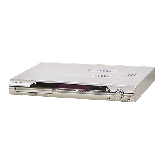
• HCD-DZ3K is the amplifier, DVD/CD
and tuner section in DAV-DZ3K.
This system incorporates with Dolby*
adaptive matrix surround decoder and the DTS*
System.
*1 Manufactured under license from Dolby Laboratories.
"Dolby," "Pro Logic," and the double-D symbol are trademarks of
Dolby Laboratories.
*2 Manufactured under license from Digital Theater Systems, Inc.
"DTS" and "DTS Digital Surround" are trademarks of Digital
Theater Systems, Inc.
Amplifier section
Latin American models:
Stereo mode (rated)
100 W + 100 W (3 ohms at
1 kHz, 1 % THD)
Surround mode (reference) RMS output power, 10 %
THD
Front: 133 W + 133 W
(with SS-TS59)
Center*: 133 W
(with SS-CT51C)
Surround*: 133 W + 133
W
(with SS-TS51C)
Subwoofer*: 135 W
(with SS-WS52)
Mexican and other models:
Stereo mode (rated)
108 W + 108 W (3 ohms at
1 kHz, 1 % THD)
Surround mode (reference) RMS output power, 10 %
THD
Front: 142 W + 142 W
(with SS-TS59)
Center*: 142 W
(with SS-CT51C)
Surround*: 142 W + 142
W
(with SS-TS51C)
Subwoofer*: 140 W
(with SS-WS52)
Sony Corporation
9-887-276-02
Home Audio Division
2006I16-1
Published by Sony Techno Create Corporation
© 2006.09
1
Digital and Dolby Pro Logic (II)
2
Digital Surround
SPECIFICATIONS
* Depending on the sound field settings and the source,
there may be no sound output.
In
puts (Analog)
TV/VCR (AUDIO IN)
AUDIO IN/MIC 1
MIC 2
DVD system
Laser
Signal format system
Mexican models:
Other models:
Tuner section
System
FM tuner section
Tuning range
Antenna (aerial)
Antenna (aerial) terminals 75 ohms, unbalanced
Intermediate frequency
HCD-DZ3K
Model Name Using Similar Mechanism
Mechanism Type
Optical Pick-up Name
AM tuner section
Tuning range
Asian and other models:
Sensitivity: 450/250 mV
Sensitivity:
AUDIO IN 250/125 mV/
Latin American models:
MIC 1 1 mV
Sensitivity: 1 mV
Antenna (aerial)
Se
miconductor laser
(DVD: λ = 650 nm)
Intermediate frequency
(CD: λ = 790 nm)
Video section
Emission duration:
Outputs
continuous
NTSC
NTSC/PAL
PLL quartz-locked digital
synthesizer system
87.5-108.0 MHz (50 kHz
step)
FM wire antenna (aerial)
10.7 MHz
E Model
Australian Model
HCD-DZ520K
CDM85-DVBU102
KHM-310CAA
531-1,602 kHz (with the
interval set at 9 kHz)
530-1,710 kHz (with the
interval set at 10 kHz)
530-1,710 kHz (with the
interval set at 10 kHz)
531-1,710 kHz (with the
interval set at 9 kHz)
AM loop antenna (aerial)
450 kHz
VIDEO: 1 Vp-p 75 ohms
S VIDEO:
Y: 1 Vp-p 75 ohms
C: 0.286 Vp-p 75 ohms
COMPONENT:
Y: 1 Vp-p 75 ohms
P
/C
, P
/C
: 0.7 Vp-p
B
B
R
R
75 ohms
— Continued on next page —
DVD RECEIVER
Advertisement
Table of Contents

Related Manuals for Sony HCD-DZ3K


Summary of Contents for Sony HCD-DZ3K
-
Page 1: Service Manual
HCD-DZ3K SERVICE MANUAL E Model Australian Model Ver. 1.1 2006.09 • HCD-DZ3K is the amplifier, DVD/CD and tuner section in DAV-DZ3K. This system incorporates with Dolby* Digital and Dolby Pro Logic (II) Model Name Using Similar Mechanism HCD-DZ520K adaptive matrix surround decoder and the DTS*... - Page 2 COMPONENTS IDENTIFIED BY MARK 0 OR DOTTED LINE WITH MARK 0 ON THE SCHEMATIC DIAGRAMS AND IN THE PARTS LIST ARE CRITICAL TO SAFE OPERATION. REPLACE THESE COMPONENTS WITH SONY PARTS WHOSE PART NUMBERS APPEAR AS SHOWN IN THIS MANUAL OR IN SUPPLEMENTS PUBLISHED BY SONY.
-
Page 3: Table Of Contents
HCD-DZ3K TABLE OF CONTENTS SERVICING NOTE 6-7. Printed Wiring Board – MAIN Board (Side B) – .... 32 ........... 4 6-8. Schematic Diagram – MAIN Board (1/10) – ....33 6-9. Schematic Diagram – MAIN Board (2/10) – ....34 GENERAL .............. -
Page 4: Servicing Note
Although this is not a Note on MAIN board replacement malfunction and for Sony service use only, New part of EEP ROM (IC1103) on the MAIN board cannot be used. normal system operation will not be possible. - Page 5 HCD-DZ3K HOW TO OPEN THE DISC TABLE WHEN POWER SWITCH TURNS OFF Insert a tapering driver into the aperture of the unit bottom, and slide it in the direction of the arrow. tapering driver loading panel Discharge the charged electricity in capacitors to prevent electric shock as follows When disassembling the machine, be sure to discharge the charged electricity in the following capacitors.
- Page 6 HCD-DZ3K Fix the capacitors with adhesive agent as follows Fixing the capacitors with adhesive agent is required by the safety regulation. Be sure to fix the capacitors with adhesive agent when part or circuit board is replaced. POWER BOARD C910...
- Page 7 HCD-DZ3K Precaution when replacing the CAP Please apply the adhesive agent to the BUTTON BASE (PLAY) when replacing the CAP (PLAY) or CAP (FUNC) or CAP (AMS). Please apply the adhesive agent to the BUTTON BASE (POWER) when replacing the CAP (POWER).
- Page 8 HCD-DZ3K Precaution on the connector processing of the POWER board. MAIN BOARD (Parts face side) IC504 CN3002 CN506 POWER BOARD AC IN (Parts face side) CN902 CN904 CN901 IC941 IC942 IC943 After twist the harness once, install the connector. MAIN board...
-
Page 9: General
HCD-DZ3K SECTION 2 This section is extracted from instruction manual. GENERAL Front panel A "/1 (on/standby) (22) (remote sensor) (8) B Front panel display (88) G MIC 2 jack (54) H VOLUME control (22) C A (open/close) (22) I AUDIO IN/MIC 1/A.CAL MIC jack (23, 54) - Page 10 HCD-DZ3K Front panel display About the indications in the front panel display A Lights up when the time information of H Lights up when the DYNAMIC BASS is a title or chapter appears in the front selected. (58) panel display. (DVD only) (38) I Lights up when CD is loaded.
-
Page 11: Remote Control
HCD-DZ3K Remote control ALPHABETICAL ORDER BUTTON DESCRIPTIONS [/1 (on/standby) 1 (14, 16, 22, A – O P – Z 30, 51) AMP MENU wg (16, 23, 53, 59, PICTURE NAVI 6 (30, 53) TV [/1 (on/standby) 1 (53) PRESET +/– wk es (51) -
Page 12: Disassembly
HCD-DZ3K SECTION 3 DISASSEMBLY 3-1. DISASSEMBLY FLOW • This set can be disassembled in the order shown below. 3-2. CASE, FRONT PANEL ASSY (Page 13) 3-9. DVD MECHANISM DECK 3-5. I/O BOARD 3-8. POWER BOARD 3-3. FL BOARD (CDM85-DVBU102) (Page 15) -
Page 13: Case, Front Panel Assy
HCD-DZ3K Note: Follow the disassembly procedure in the numerical order given. 3-2. CASE, FRONT PANEL ASSY 4 screw (CASE3 TP2) 6 five screws (+BVTP 3 × 8) 7 case 5 screw (CASE3 TP2) 9 connector (CN312) q; two screws (+BVTP 3 × 8) -
Page 14: Fl Board
HCD-DZ3K 3-3. FL BOARD 7 connector (CN811) 6 wire (flat type) 13core (CN805) 9 FL board 8 wire (flat type) 23core (CN801) 4 shield plate (fs) 3 five screws (+BVTP 2.6 × 8) 5 screw (+BVTP 2.6 × 8) 2 retainer K 1 three rivets 3-4. -
Page 15: I/O Board
HCD-DZ3K 3-5. I/O BOARD 8 I/O board qd two screws (+BV 3 × 6) 7 PWB support qf SPEAKER board When assembling, clamp the three harnesses with 6 three screws a lead pin or a similar tool so (+BVTP 3 × 8) 5 wire (flat type) that they do not touch this screw. -
Page 16: Dc Fan, Tuner Unit
HCD-DZ3K 3-7. DC FAN, TUNER UNIT 3 tuner unit 1 two screws (+BVTT 3 × 6) 4 two screws (+BVTP 3 × 8) 6 two screws (+BVTT 4 × 8) 5 cover (fan) 2 wire (flat type) 9core 7 DC fan 3-8. -
Page 17: Dvd Mechanism Deck (Cdm85-Dvbu102)
HCD-DZ3K 3-9. DVD MECHANISM DECK (CDM85-DVBU102) 7 Remove the wire and harness. 8 three screws (+BV 3 × 6) 9 cover (MD) 6 sheet q; three screws (+BV 3 × 6) 1 two screws (+BVTP 3 × 8) 5 wire (flat type) 24core... -
Page 18: Belt, Ms-203 Board
HCD-DZ3K 3-11. BELT, MS-203 BOARD 2 chuck cam 3 belt 4 screw (M 1.7 × 2.5) 1 two claws 7 MS-203 board 6 DC motor 5 three claws... -
Page 19: Optical Pick-Up (Khm-310Caa)
HCD-DZ3K 3-12. OPTICAL PICK-UP (KHM-310CAA) 3 two claws 2 chuck cam 1 two claws 4 base unit 8 two insulators 6 four insulator screws 9 two insulators 0 optical pick-up (KHM-310CAA) 5 two claws 7 bu holder... -
Page 20: Test Mode
HCD-DZ3K Ver. 1.1 SECTION 4 TEST MODE 3. Disc Tray Lock Note 1: Regarding the notification symbol “R” The disc tray lock function for the antitheft of an demonstration Because the number of the operating buttons of this product disc in the store is equipped. - Page 21 HCD-DZ3K Ver. 1.1 (2) Select “2. Drive Manual Operation” by pressing the 2 “R” DVD SECTION button on the remote commander. The screen will appear as below. 8-1. GENERAL DESCRIPTION Drive Manual Operation The IOP measurement allows you to make diagnosis and adjustment simply by using the remote commander and monitor TV.
- Page 22 HCD-DZ3K Ver. 1.1 8-4. EMERGENCY HISTORY The meaning of error code is as below: To check the emergency history, please follow the following 01: Communication error (No reply from syscon) procedure. 02: Syscon hung up 03: Power OFF request when syscon hung up (1) From the Top Menu of Remocon Diagnosis Menu, select “3.
- Page 23 HCD-DZ3K Ver. 1.1 8-4-4. Return to the Top Menu of Remocon Diagnosis Menu Press 0 “R” button on the remote commander. • Check Version Information To check the version information, please follow the following procedure. (1) From the Top Menu of Remocon Diagnosis Menu, select “4.
-
Page 24: Electrical Adjustment
HCD-DZ3K Ver. 1.1 SECTION 5 ELECTRICAL ADJUSTMENT Checking Location: MAIN board (Side A) DVD SECTION MAIN BOARD (SIDE A) When the base unit is replaced, perform the adjustment and the measurement as shown below in this order. IC501 EXECUTING IOP MEASUREMENT (See page 21) -
Page 25: Diagrams
HCD-DZ3K SECTION 6 DIAGRAMS • Circuit Boards Location THIS NOTE IS COMMON FOR PRINTED WIRING BOARDS AND SCHEMATIC DIAGRAMS. (In addition to this, the necessary note is printed in each block.) For Schematic Diagrams. For Printed Wiring Boards. Note: Note: •... -
Page 26: Block Diagram - Rf Section
HCD-DZ3K 6-1. BLOCK DIAGRAM – RF SECTION – CN1105 RFMON V2REFO V2REFO DVDRFIP TO DIAG JIG DVDA DVDB DETECTOR DVDC DVDD • Signal Path 8 NA : CD PLAY 9 NB IC1101 (1/3) OPTICAL PICK-UP : DVD PLAY CD/DVD RF AMP,... -
Page 27: Block Diagram - Audio Section
HCD-DZ3K 6-2. BLOCK DIAGRAM – AUDIO SECTION – IC352 AUDIO INPUT SELECTOR Q360-361 MUTING 11 X3 IC401 IC2200 15 X2 A/D CONVERTER 14 X1 – 1 LIN DOUT J401 – AMP LRCKO LRCK AUDIO IN/MIC 1/ AMP BCKO A.CAL MIC... -
Page 28: Block Diagram - Amp Section
HCD-DZ3K 6-3. BLOCK DIAGRAM – AMP SECTION – • Signal Path : AUDIO IC3030 IC3400 S-MASTER PROCESSOR S-MASTER DIGITAL AMP SPEAKER AMP_D1-D3 AMP_BCK0,LRCK0,MCK0 AUDIO AMP_D3 31 DATA OUTL1 14 PWMB OUTB SECTION WOOFER MCK0 (Page 27) 36 XFSIIN OUTL2 PWMA (–) -
Page 29: Block Diagram - Video Section
HCD-DZ3K 6-4. BLOCK DIAGRAM – VIDEO SECTION – IC201 VIDEO AMP, 75Ω DRIVE 2 CIN J201 COUT S VIDEO 6 YIN (DVD ONLY) YOUT 4 CVBSIN VIDEO CVBSOUT 10 CYIN 12 CBIN CYOUT CRIN J202 COMPONENT CbOUT VIDEO OUT 25 S1... -
Page 30: Block Diagram - Power Section
HCD-DZ3K 6-5. BLOCK DIAGRAM – POWER SECTION – POWER Thermistor F901 T901 D901 TRANSFORMER(MAIN) AC IN LINE T801 FILTER DC/DC D931 IC901 CONVERTER D905 +31.5V Q901 POWER VOLTAGE PROTECTION CONTROLLER IC931 VOLTAGE TO FLUORESCENT RECT DETECT INDICATOR TUBE PC901 D801,802... -
Page 31: Printed Wiring Board - Main Board (Side A)
HCD-DZ3K • See page 25 for Circuit Boards Location. 6-6. PRINTED WIRING BOARD – MAIN BOARD (SIDE A) – :Uses unleaded solder. New part of EEP ROM (IC1103) on the MAIN board cannot be used. FL BOARD Therefore, if the mounted MAIN board (A-1191-800-A, etc.) is replaced, CN801 exchange new EEP ROM (IC1103) with that used before the replacement. -
Page 32: Printed Wiring Board - Main Board (Side B)
HCD-DZ3K • See page 25 for Circuit Boards Location. 6-7. PRINTED WIRING BOARD – MAIN BOARD (SIDE B) – :Uses unleaded solder. POWER BOARD POWER BOARD CN902 CN904 (Page 49) (Page 49) (CHASSIS) (CHASSIS) (CHASSIS) IC516 C602 C3054 C512 CN515... -
Page 33: Schematic Diagram - Main Board (1/10)
HCD-DZ3K • See page 52 for IC Block Diagrams. 6-8. SCHEMATIC DIAGRAM – MAIN BOARD (1/10) – (CHASSIS) EB3001 TERMINAL BOARD R3060 R3062 R3063 R3064 R3059 TP3003 R3065 C3035 C3034 TP3004 ICT3063 R3066 R3067 R3068 R3069 R3070 R3071 TP3031 R3031... -
Page 34: Schematic Diagram - Main Board (2/10)
HCD-DZ3K • See page 53 for IC Block Diagrams. 6-9. SCHEMATIC DIAGRAM – MAIN BOARD (2/10) – ICT3010 C3406 C3403 0.033 ICT3011 0.1 16V C3551 1 50V ICT3060 R3061 R3403 TP3410 C3413 C3412 R3404 R3551 ICT3061 100k 1/10W R3402 100... -
Page 35: Schematic Diagram - Main Board (3/10)
HCD-DZ3K • See page 51 for Waveform. • See page 52 for IC Block Diagrams. 6-10. SCHEMATIC DIAGRAM – MAIN BOARD (3/10) – R3055 C3015 C3014 R3011 470 1/10W R3012 1/10W TP3011 R3151 R3013 1/10W TP3012 C3013 25V F R3014... -
Page 36: Schematic Diagram - Main Board (4/10)
HCD-DZ3K • See page 53 for IC Block Diagrams. 6-11. SCHEMATIC DIAGRAM – MAIN BOARD (4/10) – Q3202 Q3252 2SA1235TP-1EF 2SA1235TP-1EF ICT3027 C3206 C3203 0.033 Q3201 Q3251 2SA1235TP-1EF ICT3028 2SA1235TP-1EF R3203 C3213 TP3210 C3212 C3221 C3271 R3204 R3207 C3215 C3220 0.0022... -
Page 37: Schematic Diagram - Main Board (5/10)
HCD-DZ3K • See page 51 for Waveform. • See page 56 for IC Pin Function Description. 6-12. SCHEMATIC DIAGRAM – MAIN BOARD (5/10) – 1k : SP 10k : E32, MX 15k : AUS 47k : AUS 47k : E32, MX... -
Page 38: Schematic Diagram - Main Board (6/10)
HCD-DZ3K 6-13. SCHEMATIC DIAGRAM – MAIN BOARD (6/10) – C582 IC516 IC TA7805LS C580 2200 6.3V C601 C602 C603 100 10V C517 0.001 C525 C506 C598 C510 C511 R506 C504 FB501 C507 C505 Q502 RSR025N03 FL501 FL502 R507 FB503 FB508... -
Page 39: Schematic Diagram - Main Board (7/10)
HCD-DZ3K 6-14. SCHEMATIC DIAGRAM – MAIN BOARD (7/10) – IC1107 TK11133CSC L-G ICT1129 C1193 C1195 0.22 0.22 C1192 FL1101 0.01 25V B C1101 CN1101 0.01 JL1139 C1120 1 10V B JL1140 C1121 1 10V B C1122 1 10V B C1123... -
Page 40: Schematic Diagram - Main Board (8/10)
HCD-DZ3K • See page 51 for Waveforms. • See page 59 for IC Pin Function Description. 6-15. SCHEMATIC DIAGRAM – MAIN BOARD (8/10) – R2120 R2121 R2122 R2123 C1163 R2124 C1137 C1139 C1140 C1146 C1161 0.01 0.01 R2125 R1136 C1132... -
Page 41: Schematic Diagram - Main Board (9/10)
HCD-DZ3K Ver. 1.1 6-16. SCHEMATIC DIAGRAM – MAIN BOARD (9/10) – New part of EEP ROM (IC1103) on the MAIN board cannot be used. Therefore, if the mounted MAIN board (A-1191-800-A, etc.) is replaced, exchange new EEP ROM (IC1103) with that used before the replacement. -
Page 42: Schematic Diagram - Main Board (10/10)
HCD-DZ3K 6-17. SCHEMATIC DIAGRAM – MAIN BOARD (10/10) – R1234 ICT550 R1223 R1225 100k 100k 1/10W 1/10W 0.5% 0.5% C1209 R1230 0.033 1/10W C1228 C1212 0.5% 0.0047 0.01 R1221 1/10W 0.5% R1220 C1214 ICT551 0.001 C1215 ICT549 0.01 25V B... -
Page 43: Printed Wiring Board - I/O Board
HCD-DZ3K • See page 25 for Circuit Boards Location. 6-18. PRINTED WIRING BOARD – I/O BOARD – :Uses unleaded solder. I/O BOARD J202 J200 COMPONENT TV/VCR J201 S VIDEO VIDEO OUT MONITOR (DVD ONLY) AUDIO IN VIDEO C242 C354 C224... -
Page 44: Schematic Diagram - I/O Board
HCD-DZ3K • See page 51 for Waveforms. • See page 54 for IC Block Diagrams. 6-19. SCHEMATIC DIAGRAM – I/O BOARD – C374 R396 C399 100 16V 1 50V R388 220 1W D212 D211 R340 1SS355 1SS355TE-17 TE-17 R387 C397 8.2k... -
Page 45: Printed Wiring Boards - Panel Section
HCD-DZ3K • See page 25 for Circuit Boards Location. 6-20. PRINTED WIRING BOARDS – PANEL SECTION – :Uses unleaded solder. S801 I/O BOARD CN302 S800 (Page 43) VOLUME – CN804 FB410 FB420 C820 R403 R416 FB472 CNP802 R434 C434 C819... -
Page 46: Schematic Diagram - Panel Section
HCD-DZ3K • See page 55 for IC Block Diagram. 6-21. SCHEMATIC DIAGRAM – PANEL SECTION – CNP807 CHASSIS GND CN402 S800 TP402 VOLUME KNOB TP409 FB410 TP400 C819 C820 0.01 0.01 TP410 TP418 R821 R822 TP412 BOARD CN312 FB470 (Page 44) -
Page 47: Printed Wiring Board - Speaker Board
HCD-DZ3K • See page 25 for Circuit Boards Location. 6-22. PRINTED WIRING BOARD – SPEAKER BOARD – 6-23. SCHEMATIC DIAGRAM – SPEAKER BOARD – :Uses unleaded solder. SPEAKER BOARD MAIN BOARD MAIN BOARD MAIN BOARD EP301 CN3200 CN3300 CN3100 EARTH PLATE... -
Page 48: Printed Wiring Board - Ms-203 Board
HCD-DZ3K • See page 25 for Circuit Boards Location. 6-24. PRINTED WIRING BOARD – MS-203 BOARD – 6-25. SCHEMATIC DIAGRAM – MS-203 BOARD – :Uses unleaded solder. MS-203 BOARD CN001 S001 (CHUCK/TRAY DETECT) MAIN CN001 BOARD CN1202 (Page 32) 1-861-327- 12... -
Page 49: Printed Wiring Board - Power Board
HCD-DZ3K • See page 25 for Circuit Boards Location. 6-26. PRINTED WIRING BOARD – POWER BOARD – :Uses unleaded solder. • Semiconductor (CHASSIS) Location R969 Ref. No. Location D906 D907 EB902 R906 R926 R925 D901 B-11 C907 D908 D905 IC901... -
Page 50: Schematic Diagram - Power Board
HCD-DZ3K 6-27. SCHEMATIC DIAGRAM – POWER BOARD – D931 FCU20UC20 C938 1.8k : E32 EXCEPT CN902 (CHASSIS) 3.3k : EXCEPT E32 TP903 WIRE 3P CN901 TH901 FH901 FH902 C965 C963 0.001 THERMISTOR, HOLDER HOLDER D901 C930 L931 TP901 T901 R931... - Page 51 HCD-DZ3K • Waveforms – I/O Board – – MAIN Board – IC1101 6 (DVDRFIP) IC201 wh (COUT) IC201 qk (CbOUT) 2.0 Vp-p 1.6 Vp-p 900 mVp-p 500 mV/DIV, 20 µ s/DIV 1 V/DIV, 20 µ s/DIV 200 mV/DIV, 100 ns/DIV IC1101 <xx.
-
Page 52: Ic Block Diagrams
HCD-DZ3K • IC Block Diagrams – MAIN Board – IC2200 PCM1803DBR 5 th Order Single-End MODE1 Delta-Sigma VINL 1 /Differential Modulator MODE0 VINR 2 Converter Serial FMT1 VERF1 3 Interface FMT0 VERF2 4 × 1/64 (× 1/128) Decimation Filter Reference... - Page 53 HCD-DZ3K – MAIN Board – IC3050 TK1118CSCL-G OVER HEAT & OVER CURRENT PROTECTION CONTROL CIRCUIT BANDGAP REFERENCE IC3100, IC3150, IC3200, IC3250, IC3300, IC3400 CXD9883M BST_A PVDD_A Over Current Fault GVDD_A PVDD_A /OTW PVDD_A VREG Gate Drive /HIZ_HS_A PGND /HIZ_LS_A Stuck...
- Page 54 HCD-DZ3K – I/O Board – IC352 MC14052BDR2 IC357 M62429FP-TP VIN2 VOUT2 CLOCK VR 2 VOL AMP 2 VREF LOGIC CONTROL VOL AMP 1 REF AMP VR 1 VIN1 VOUT1 DATA IC201 MM1623BFBE S-DC OUT 28 VCC2 S1/S2 27 S-DC OUT 150kΩ...
- Page 55 HCD-DZ3K – FL Board – IC802 uPD16315GB-3BS Grid driver Multiplexed driver SEG19/GRID10 Command decoder LED1 SEG18/GRID11 LED2 Display memory LED3 SEG17/GRID12 24 bits x 12 words LED4 Timing generator key scan DOUT SEG16/KS16 Key data memory Serial SEG15/KS15 (2 x 16 bits)
- Page 56 HCD-DZ3K • IC Pin Function Description MAIN BOARD IC501 M30622MEP-A76FPU0 (SYSTEM CONTROLLER) Pin No. Pin Name Description DAMP_SCDT/ DAMP processor and Diat data output DIAT_SDATA DAMP_SHIFT/ DAMP processor and Diat clock output DIAT_SCLK DSP_INTR DSP interrupt (not used) SIRCS_IN Sircs input...
- Page 57 HCD-DZ3K Pin No. Pin Name Description OVERFLOW1 DAMP processor F/C/S over flow detect OVERFLOW2 DAMP processor SW over flow detect WRITE CE Flash write CE (not used) DAMP LATCH1 DAMP processor latch1 DAMP LATCH2 DAMP processor latch2 DAMP LATCH3 DAMP processor latch3...
- Page 58 HCD-DZ3K Pin No. Pin Name Description IO_CLK I/O expander IC clock output (not used) MONO/ST_DET Front jack MONO or STEREO detect A.CAL MIC LEVEL MIC level detect for auto calibration DESTINATION Destination select input MODEL Model select input KEY2 Key input 2 input...
- Page 59 HCD-DZ3K MAIN BOARD IC1101 CXD9849R (CD/DVD RF AMP, FOCUS/TRACKING ERROR AMP, DVD SYSTEM PROCESSOR, DIGITAL SERVO PROCESSOR) Pin No. Pin Name Description AGND — Ground terminal DVDA AC coupled input path A DVDB AC coupled input path B DVDC AC coupled input path C...
- Page 60 HCD-DZ3K Pin No. Pin Name Description DSEL — Not used WIDE Wide switch signal output terminal Mute signal control output MAMUTE MAMUTE signal output to system controller (IC501) (not used) DVDD18 — Power supply (+1.8V from IC1109) 53 to 58...
- Page 61 HCD-DZ3K Pin No. Pin Name Description DQMO DQM0 signal output to SD-RAM (IC1104) MREQ DQM signal input (not used) Data bus 7 from SD-RAM (IC1104) DVSS — Ground terminal 117, 118 RD 6, 5 Data bus 6, 5 from SD-RAM (IC1104) DVSS —...
- Page 62 HCD-DZ3K Pin No. Pin Name Description LIMSW LIMSW signal output to optical pick-up OCSW SEN signal input from system controller (IC501)/OCSW signal input REW signal output to IC1201 CKSW CKSW signal input — Not used — Not used DVDD3 —...
- Page 63 HCD-DZ3K Pin No. Pin Name Description SDPIF — SPDIF output (not used) RFGND18 — Ground terminal RFVDD18 — Power supply (RF+1.8V) XTALO Oscillator output signal (27MHz) XTALI Oscillator input signal (27MHz) JITFO RF jitter meter output JITFN Negative input of operation amplifier for RF jigger meter PLLVSS —...
-
Page 64: Exploded Views
HCD-DZ3K SECTION 7 EXPLODED VIEWS NOTE: • -XX and -X mean standardized parts, so they • The mechanical parts with no reference The components identified by mark 0 or may have some difference from the original number in the exploded views are not supplied. -
Page 65: Front Panel Section
2-652-984-01 WINDOW, INDICATION 1-828-325-11 WIRE(FLAT TYPE)(13 CORE) 2-652-979-01 ORNAMENT (POWER) 2-652-973-01 CAP (POWER) 2-661-952-01 SHEET (WINDOW), ADHESIVE 2-652-974-01 CAP (PLAY) 3-943-995-31 EMBLEM (NO.5), SONY 2-652-975-01 CAP (FUNC) 2-652-977-01 BUTTON BASE (POWER) 2-652-976-01 CAP (AMS) 2-652-971-63 PANEL, FRONT 3-531-576-01 RIVET 3-087-053-01 +BVTP2.6 (3CR) Note: If the wire (flat type) was replaced, fold it some as the wire (flat type) before replacement. -
Page 66: Chassis Section
HCD-DZ3K 7-3. CHASSIS SECTION supplied supplied supplied supplied supplied supplied supplied supplied supplied supplied F901 DVD mechanism deck section (CDM85-DVBU102) supplied not supplied not supplied Ref. No. Part No. Description Remark Ref. No. Part No. Description Remark 3-077-331-21 +BV3 (3-CR) -
Page 67: Dvd Mechanism Deck Section (Cdm85-Dvbu102)
HCD-DZ3K 7-4. DVD MECHANISM DECK SECTION (CDM85-DVBU102) not supplied not supplied not supplied not supplied not supplied not supplied not supplied not supplied supplied Ref. No. Part No. Description Remark Ref. No. Part No. Description Remark A-6071-669-A LOADING ASSY (M) -
Page 68: Electrical Parts List
HCD-DZ3K SECTION 8 DDCON ELECTRICAL PARTS LIST NOTE: • Due to standardization, replacements in the • COILS When indicating parts by reference number, parts list may be different from the parts uH: µH please include the board name. specified in the diagrams or the components •... - Page 69 HCD-DZ3K Ref. No. Part No. Description Remark Ref. No. Part No. Description Remark R811 1-216-844-11 METAL CHIP 1/10W C357 1-162-927-11 CERAMIC CHIP 100PF R812 1-216-845-11 METAL CHIP 100K 1/10W C358 1-162-927-11 CERAMIC CHIP 100PF C359 1-126-960-11 ELECT R813 1-216-845-11 METAL CHIP...
- Page 70 HCD-DZ3K JACK Ref. No. Part No. Description Remark Ref. No. Part No. Description Remark < TRANSISTOR > R369 1-216-821-11 METAL CHIP 1/10W R370 1-216-833-11 METAL CHIP 1/10W Q351 8-729-027-52 TRANSISTOR DTC124EKA-T146 R371 1-216-833-11 METAL CHIP 1/10W Q353 8-729-027-52 TRANSISTOR DTC124EKA-T146...
- Page 71 HCD-DZ3K JACK Ref. No. Part No. Description Remark Ref. No. Part No. Description Remark < CONNECTOR > R404 1-216-829-11 METAL CHIP 4.7K 1/10W R405 1-216-829-11 METAL CHIP 4.7K 1/10W CNP802 1-779-550-21 CONNECTOR, FFC (LIF (NON-ZIF)) 13P R410 1-216-845-11 METAL CHIP...
- Page 72 HCD-DZ3K JACK MAIN Ref. No. Part No. Description Remark Ref. No. Part No. Description Remark S806 1-762-875-21 SWITCH, KEYBOARD (>) C1120 1-165-908-11 CERAMIC CHIP S807 1-762-875-21 SWITCH, KEYBOARD (A) C1121 1-165-908-11 CERAMIC CHIP S808 1-762-875-21 SWITCH, KEYBOARD (H) C1122 1-165-908-11 CERAMIC CHIP...
- Page 73 HCD-DZ3K MAIN Ref. No. Part No. Description Remark Ref. No. Part No. Description Remark C1191 1-107-826-11 CERAMIC CHIP 0.1uF C3025 1-164-156-11 CERAMIC CHIP 0.1uF C1192 1-162-970-11 CERAMIC CHIP 0.01uF C3026 1-164-156-11 CERAMIC CHIP 0.1uF C1193 1-127-715-91 CERAMIC CHIP 0.22uF C1195 1-127-715-91 CERAMIC CHIP 0.22uF...
- Page 74 HCD-DZ3K MAIN Ref. No. Part No. Description Remark Ref. No. Part No. Description Remark C3155 1-107-725-11 CERAMIC CHIP 0.1uF C3303 1-107-725-11 CERAMIC CHIP 0.1uF C3156 1-115-185-11 CERAMIC CHIP 0.033uF C3304 1-164-156-11 CERAMIC CHIP 0.1uF C3157 1-115-185-11 CERAMIC CHIP 0.033uF C3158 1-104-329-11 CERAMIC CHIP 0.1uF...
- Page 75 HCD-DZ3K Ver. 1.1 MAIN Ref. No. Part No. Description Remark Ref. No. Part No. Description Remark D504 6-501-193-01 DIODE 1SS355WTE-17 FL1108 1-234-177-21 FILTER, CHIP EMI D505 6-501-193-01 DIODE 1SS355WTE-17 D2001 8-719-058-24 DIODE RB501V-40TE-17 < IC > D3071 6-501-193-01 DIODE 1SS355WTE-17...
- Page 76 HCD-DZ3K MAIN Ref. No. Part No. Description Remark Ref. No. Part No. Description Remark < TRANSISTOR > R620 1-216-809-11 METAL CHIP 1/10W R622 1-216-833-11 METAL CHIP 1/10W Q502 6-550-718-01 TRANSISTOR RSR025N03TL R624 1-216-833-11 METAL CHIP 1/10W Q506 8-729-120-28 TRANSISTOR 2SC1623-L5L6...
- Page 77 HCD-DZ3K MAIN Ref. No. Part No. Description Remark Ref. No. Part No. Description Remark R1116 1-216-821-11 METAL CHIP 1/10W R1228 1-216-864-11 SHORT CHIP R1117 1-216-841-11 METAL CHIP 1/10W R1118 1-216-801-11 METAL CHIP 1/10W R1230 1-218-893-11 METAL CHIP 0.5% 1/10W R1120...
- Page 78 HCD-DZ3K MAIN Ref. No. Part No. Description Remark Ref. No. Part No. Description Remark R2506 1-216-864-11 SHORT CHIP R3101 1-216-809-11 METAL CHIP 1/10W R2546 1-216-827-11 METAL CHIP 3.3K 1/10W R2547 1-216-829-11 METAL CHIP 4.7K 1/10W R3102 1-216-809-11 METAL CHIP 1/10W...
- Page 79 HCD-DZ3K MAIN MS-203 POWER Ref. No. Part No. Description Remark Ref. No. Part No. Description Remark R3271 1-216-833-11 METAL CHIP 1/10W R3272 1-216-833-11 METAL CHIP 1/10W < VIBRATOR > R3273 1-216-833-11 METAL CHIP 1/10W R3274 1-216-833-11 METAL CHIP 1/10W X502...
- Page 80 HCD-DZ3K POWER Ref. No. Part No. Description Remark Ref. No. Part No. Description Remark 0 C928 1-113-900-11 CERAMIC 470PF 250V 0 D909 6-501-193-01 DIODE 1SS355WTE-17 0 D910 (EXCEPT MX) 6-501-193-01 DIODE 1SS355WTE-17 0 D913 6-500-241-01 DIODE SARS03 0 C929 1-115-339-11 CERAMIC CHIP 0.1uF...
- Page 81 HCD-DZ3K POWER SPEAKER Ref. No. Part No. Description Remark Ref. No. Part No. Description Remark < IC > R936 1-216-853-11 METAL CHIP 470K 1/10W R937 1-216-833-11 METAL CHIP 1/10W 0 PC901 6-600-438-01 IC TLP421F (D4-GR) R938 1-216-821-11 METAL CHIP 1/10W...
- Page 82 HCD-DZ3K SPEAKER Ref. No. Part No. Description Remark C316 1-163-021-91 CERAMIC CHIP 0.01uF C317 1-163-021-91 CERAMIC CHIP 0.01uF C318 1-163-021-91 CERAMIC CHIP 0.01uF C319 1-163-021-91 CERAMIC CHIP 0.01uF C320 1-163-021-91 CERAMIC CHIP 0.01uF C321 1-163-021-91 CERAMIC CHIP 0.01uF C322 1-163-021-91 CERAMIC CHIP 0.01uF...
- Page 83 HCD-DZ3K MEMO...
-
Page 84: Revision History
HCD-DZ3K REVISION HISTORY Clicking the version allows you to jump to the revised page. Also, clicking the version at the upper right on the revised page allows you to jump to the next revised page. Ver. Date Description of Revision 2006.06...