Table of Contents
Advertisement
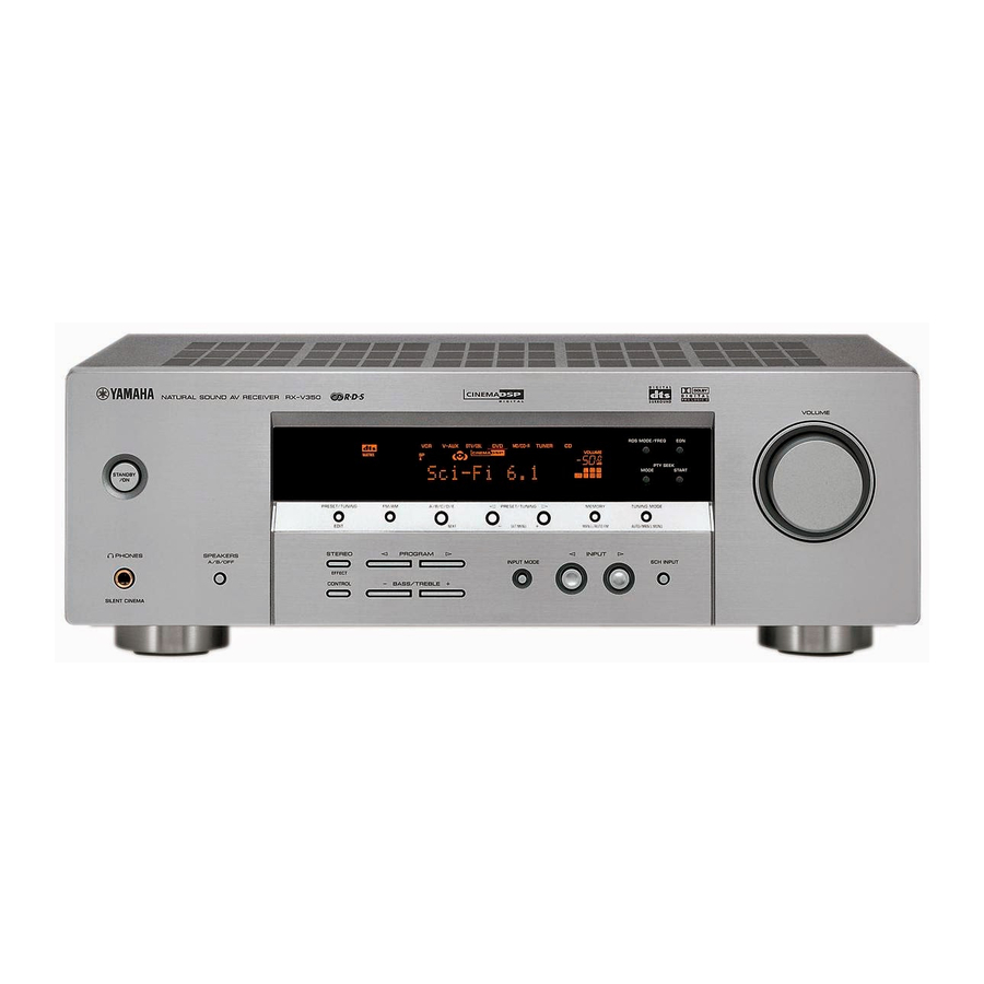
RX-V350/HTR-5730
This manual has been provided for the use of authorized YAMAHA Retailers and their service personnel.
It has been assumed that basic service procedures inherent to the industry, and more specifically YAMAHA Products, are already
known and understood by the users, and have therefore not been restated.
WARNING:
IMPORTANT:
The data provided is believed to be accurate and applicable to the unit(s) indicated on the cover. The research, engineering, and
service departments of YAMAHA are continually striving to improve YAMAHA products. Modifications are, therefore, inevitable
and specifications are subject to change without notice or obligation to retrofit. Should any discrepancy appear to exist, please
contact the distributor's Service Division.
WARNING:
IMPORTANT:
I CONTENTS
TO SERVICE PERSONNEL .......................................... 2
FRONT PANELS ........................................................ 3~4
REAR PANELS .......................................................... 4~8
REMOTE CONTROL PANELS ...................................... 8
SPECIFICATIONS .................................................... 9~11
INTERNAL VIEW ......................................................... 12
DISASSEMBLY PROCEDURES ........................... 12~14
Self Diagnosis Function (Diag) ................. 15~31
Confirmation Of Idling Current ................... 32
1 0 0 8 8 3
SERVICE MANUAL
IMPORTANT NOTICE
Failure to follow appropriate service and safety procedures when servicing this product may result in personal
injury, destruction of expensive components, and failure of the product to perform as specified. For these reasons,
we advise all YAMAHA product owners that any service required should be performed by an authorized
YAMAHA Retailer or the appointed service representative.
The presentation or sale of this manual to any individual or firm does not constitute authorization, certification or
recognition of any applicable technical capabilities, or establish a principle-agent relationship of any form.
Static discharges can destroy expensive components. Discharge any static electricity your body may have
accumulated by grounding yourself to the ground buss in the unit (heavy gauge black wires connect to this buss).
Turn the unit OFF during disassembly and part replacement. Recheck all work before you apply power to the unit.
Display Data ..................................................... 33~34
Ic Data ................................................................. 35~40
PRINTED CIRCUIT BOARD .................................. 41~48
Pin Connection Diagram .............................. 49~50
Block Diagram ....................................................... 51
Schematic Diagram ........................................ 52~56
Parts List ........................................................... 57~71
REMOTE CONTROL .............................................. 72~73
AV RECEIVER
P.O.Box 1, Hamamatsu, Japan
Advertisement
Table of Contents

Related Manuals for Yamaha RX-V350


Summary of Contents for Yamaha RX-V350
-
Page 1: Service Manual
This manual has been provided for the use of authorized YAMAHA Retailers and their service personnel. It has been assumed that basic service procedures inherent to the industry, and more specifically YAMAHA Products, are already known and understood by the users, and have therefore not been restated. - Page 2 RX-V350/HTR-5730 I SELF DIAGNOSIS FUNCTION (DIAG) There are 15 DIAG menu items, each of which has sub-menu items. Listed in the table below are menu items and sub-menu items. Note that not all menu items listed will apply to the models covered in this service manual.
- Page 3 RX-V350/HTR-5730 No DIAG menu sub-menu 11 IF STATUS 1. INSIDE STATUS 1 (5 Byte) 2. INSIDE STATUS 2 (3 Byte) 3. CHANNEL STATUS 1 (5 Byte) 4. CHANNEL STATUS 2 (5 Byte) 5. CHANNEL STATUS 3 (5 Byte) 6. CHANNEL STATUS 4 (5 Byte) 7.
- Page 4 RX-V350/HTR-5730 • Starting DIAG • Display provided when DIAG started Press the “STANDBY/ON” key while simultaneously The FL display of the main unit displays the protection pressing those two keys of the main unit as indicated in the function history data and the version (1 alphabet) and the figure below.
- Page 5 RX-V350/HTR-5730 • Operation procedure of DIAG menu and When there is a history of protection Version (1 alphabet) function due to abnormal DC output SUB-MENU There are 15 MENU items, each of which has some SUB- MENU items. DIAG menu selection Cause: DC output of the power amplifier is abnormal.
- Page 6 RX-V350/HTR-5730 • Details of DIAG menu YSS Presence 0dB • The Presence CH signal including the head margin is With full-bit output specified in some modes, it is possible output at the Front CH. to execute 0dBFS output without including the head Head margin: margin in each channel.
- Page 7 RX-V350/HTR-5730 YSS FULL BIT P • The Presence CH signal is output in digital full bit at the Front CH. Reference data INPUT: DVD ANALOG SWFR: 50Hz, Others: 1kHz SPEAKER OUTPUT ( 1kHz ) SUBWOOFER Input level Volume FRONT OUTPUT...
- Page 8 RX-V350/HTR-5730 2. RAM THROUGH This function is for YSS938 only. Only the CT signal is output through the Sub DSP – DRAM. RAM 0dB Reference data INPUT: DVD ANALOG SWFR: 50Hz, Others: 1kHz SPEAKER OUTPUT ( 1kHz ) SUBWOOFER Input level...
- Page 9 RX-V350/HTR-5730 3. PRO LOGIC PRO LOGIC I PRO LOGIC II Reference data Reference data INPUT: DVD ANALOG INPUT: DVD ANALOG SWFR: 50Hz, Others: 1kHz SWFR: 50Hz, Others: 1kHz SPEAKER OUTPUT ( 1kHz ) SUBWOOFER SPEAKER OUTPUT ( 1kHz ) SUBWOOFER...
- Page 10 RX-V350/HTR-5730 4. SPEAKERS SET The input signal is automatically identified and switched in The signals output from the DSP block are the same as 1. the priority order of dts → DOLBY DIGITAL → AAC → DSP THROUGH: YSS 0dB.
- Page 11 RX-V350/HTR-5730 5. HP Test The signal is output including the head margin. FRONT 15dB MARGIN FRONT 12dB MARGIN Reference data Reference data INPUT: DVD ANALOG INPUT: DVD ANALOG SWFR: 50Hz, Others: 1kHz SWFR: 50Hz, Others: 1kHz SPEAKER OUTPUT ( 1kHz ) SUBWOOFER...
- Page 12 RX-V350/HTR-5730 7. DISPLAY CHECK Segment conditions of the FL driver and the FL tube are This program is used to check the FL display section. The checked by turning ON and OFF all segments. Next, the display condition varies as shown below according to the operation of the FL driver is checked by using the dimmer sub-menu operation.
- Page 13 RX-V350/HTR-5730 9. FACTORY PRESET This menu is used to reserve and inhibit initialization of the back-up RAM. The signals are processed using EFFECT OFF. (The L/R signal is output using ANALOG FRONT BYPASS.) PRESET INHIBIT (Initialization inhibited) RAM initialization is not executed. Select this sub-menu to protect the values set by the user.
- Page 14 RX-V350/HTR-5730 10. AD DATA CHECK/FAN TEST K0/K1 (Panel key of main unit) This menu is used to display the A/D conversion value of A/D of the key fails to function properly when the standard the terminals which detects panel keys of the main unit value is deviated.
- Page 15 RX-V350/HTR-5730 11. IF STATUS (Input function status) Using the sub-menu, the status data is displayed one after another in the hexadecimal notation. 5th byte During signal processing, the status before execution of 4th byte this menu is maintained. 3rd byte * Numeric values in the figure example are for reference.
- Page 16 RX-V350/HTR-5730 CS1-5: Indicates channel status information of the input MTT: Mute Trigger signal (IEC60958). Byte No. Function Mute condition Factor of the last mute BY1-4: Indicates information of the bit stream included in Error count of YSS938-FSCNT the DOLBY DIGITAL signal.
- Page 17 RX-V350/HTR-5730 13. SD DL CODE 14. SOFT SW This menu is used to display the data version of the This menu is used to switch the function settings on the FLASH ROM, TOC information and sum calculated P.C.B. through the software so as to activate the product.
- Page 18 RX-V350/HTR-5730 15. MICROPROCESSOR INFORMATION The version, checksum and the port specified by the microprocessor are displayed. The signal is processed using EFFECT OFF. The checksum is obtained by adding the data at every 8 bits for each program area and expressing the result as a 4-figure hexadecimal data.
- Page 19 RX-V350/HTR-5730 I CONFIRMATION OF IDLING CURRENT Confirmation of Idling Current of Main (1) P. C. B. • Right after the power is turned on, confirm that the voltage across the terminals of R157 (Front Lch), R158 (Front Rch), R148 (Center), R156 (Surround Lch), R159 (Surround Rch) are between 0.1mV and 10.0mV.
-
Page 20: Display Data
RX-V350/HTR-5730 I DISPLAY DATA G V851 : 16-BT-122GNK (WC173100) PATTERN AREA G PIN CONNECTION Pin No. Connection Pin No. Connection Note : 1) F1, F2 ..Filament 2) NP ..No pin 3) NX ..No extened 4) DL ..Datum line 5) 1G ~ 16G .. - Page 21 RX-V350/HTR-5730 G ANODE CONNECTION 9G~5G – – – – – – – – – – – – – – – – – – – –...
- Page 22 RX-V350/HTR-5730 I IC DATA IC242: M30626FHPFP (MAIN P.C.B.) 16bit µ-COM (Main CPU) P07/D7 P44/CS0 P06/D6 P45/CS1 P05/D5 P46/CS2 P04/D4 P47/CS3 P03/D3 P50/WRL/WR P02/D2 P51/WRH/BHE P01/D1 P52/RD P00/D0 P53/BCLK P107/AN7 P54/HLDA P106/AN6 P55/HOLD P105/AN5 P56/ALE P104/AN4 P57/RDY/CLKOUT P103/AN3 P60/CTS0/RTS0 P102/AN2 P61/CLK0...
- Page 23 RX-V350/HTR-5730 IC242: M30626FHPFP (MAIN P.C.B.) 16bit µ-COM (Main CPU) Port No. Function name Detail of function /ICCS CS493x Reset (Unconnected) /CSPLD Digital External Control IC CE (Unconnected) For Flash Writing (HI) CSINT CS-DSP INT/ABOOT (Unconnected) /FMT Mute Front /CMT Mute Center...
- Page 24 RX-V350/HTR-5730 IC801 : YSS938 (DSP P.C.B.) RAMA9 RAMA3 SELI1 RAMA4 SELI0 SELI9 SELOA SELI10 SELOB SELI11 TESTMS SELI12 SELI13 TESTXEN IPORT0 RAMA2 IPORT1 RAMA5 IPORT2 RAMA1 IPORT3 RAMA6 IPORT4 RAMA0 DDIN0 RAMA7 DDIN1 RAMA8 DDIN2 VDD1 DDIN3 RASN RAMOEN YSS938...
- Page 25 RX-V350/HTR-5730 IC801 : YSS938 (DSP P.C.B.) Name Function Crystal oscillator connecting terminal Crystal oscillator connecting terminal (24.576MHz) SELI1 Built-in selector input 1 (AXD) (Unconnected) SELI0 Built-in selector input 0 (GND) SELOA Built-in selector output A (ISEL) SELOB Built-in selector output B...
- Page 26 RX-V350/HTR-5730 IC801 : YSS938 (DSP P.C.B.) Name Function SDWCKI1 Word clock input terminal for SDIB, SDOB interface (WCKG) (Unconnected) SDBCKI1 Bit clock input terminal for SDIB, SDOB interface (BCKG) (Unconnected) Ground terminal SDOB3 PCM output terminal from Sub DSP SDOB2...
- Page 27 RX-V350/HTR-5730 IC801 : YSS938 (DSP P.C.B.) Name Function RAMA5 Sub DSP: External memory address terminal 5 RAMA2 Sub DSP: External memory address terminal 2 SELI13 Built-in selector input 13 (Unconnected) SELI12 Built-in selector input 12 (Unconnected) SELI11 Built-in selector input 11...
-
Page 28: Pin Connection Diagram
RX-V350/HTR-5730 I PIN CONNECTION DIAGRAM • ICs µPC29M33T-E1 KIA7805API KIA7912PI PQ025EZ5MZP NJM2068MD LA7956 MM74HCU04SJX KIA7812API TC74HCT08AF 3: IN 2: COM 1: OUT LC72722PM AK4628VQ TC74HCT08AF M66003-0101FP MSM514260E-60JS BD3816K1 STK403-130Y STK404-130Y M30626FHPFP YSS938... - Page 29 RX-V350/HTR-5730 • Diodes 1SS133 MTZJ20B 1SS355 1SS270A MTZJ4.7A MA8075-H Anode MTZJ30A UDZ5.1B Anode MTZJ20A UDZ6.8B UDZS5.6BTE-17 UDZS6.2B Cathode UDZS9.1B Cathode KDS160-RTK TS6P03G KBP103G SB01-05Q Cathode – – Anode • Transistors 2SA1015 2SC1740S 2SB1274 2SB949 KRA104M-AT 2SD1913 2SC1815 KRC102M-AT 2SC2705 2SA2N5401C-AT...
- Page 30 RX-V350/HTR-5730 BLOCK DIAGRAM • See page 56 → SCHEMATIC DIAGRAM MAIN INPUT SELECTOR MONITOR IC391 D-TV/CBL V-AUX • See page 56 → SCHEMATIC DIAGRAM • See page 52 → SCHEMATIC DIAGRAM MAIN Q391~393 C377 XL801 POWER LIMIT RY371 F371 24.576MHz...
- Page 31 RX-V350/HTR-5730 SCHEMATIC DIAGRAM (DSP) Page 56 Page 53 to MAIN (1) to FUNCTION (1) REGULATOR 4M DRAM CONVERTER CENTER LEVEL CONVERT & SURROUND L SIGNAL DETECT FRONT L IC805: µPC29M33T-E1 IC802: MSM514260E-60JS IC803: AK4628VQ IC804: PQ025EZ5MZP IC806: TC74HCT08AF IC807: MM74HCU04SJX...
- Page 32 RX-V350/HTR-5730 SCHEMATIC DIAGRAM (FUNCTION 1/2) Page 56 Page 52 to MAIN (1) to DSP FUNCTION (1) 12.0 FRONT L -12.1 12.0 12.1 FUNCTION (6) CENTER -12.1 12.0 SURROUND L -7.7 -7.7 -7.0 -12.1 -12.1 FRONT L 12.0 CD L (ANALOG IN) INPUT SELECT &...
- Page 33 RX-V350/HTR-5730 SCHEMATIC DIAGRAM (FUNCTION 2/2) FL DISPLAY -14.7 -7.2 -14.6 -7.2 -26.2 -24.3 -26.3 -22.4 -22.2 -22.2 x: NOT USED -7.2 -7.4 O: USED / APPLICABLE FL DISPLAY -28.1 -18.5 -9.0 -26.2 DRIVER -28.3 FUNCTION (5) -28.3 -22.3 -10.9 -10.9 -16.7...
- Page 34 RX-V350/HTR-5730 SCHEMATIC DIAGRAM (MAIN 1/2) L CH POWER AMP 49.2 49.1 MUTE SURROUND L DETECT -12.1 48.9 -12.1 0 SURROUND L FRONT L DETECT 48.9 48.9 47.2 47.8 47.2 47.8 29.1 DETECT FRONT L R CH POWER AMP MUTE DETECT MAIN (4) 48.9...
- Page 35 RX-V350/HTR-5730 SCHEMATIC DIAGRAM (MAIN 2/2) Point 2 Pin 12 of IC241 Point 3 Pin 13 of IC242 Point 4 emitter of Q258 and collector of Q259 MAIN (3) INPUT A Q258 E SELECTOR B Q259 C POWER ON POWER OFF...
-
Page 36: Parts List
RX-V350/HTR-5730 PARTS LIST I ELECTRICAL PARTS I WARNING Components having special characteristics are marked s and must be replaced with parts having specifications equal to those originally installed. ABBREVIATIONS IN THIS LIST ARE AS FOLLOWS: C.A.EL.CHP : CHIP ALUMI.ELECTROLYTIC CAP L.EMIT... - Page 37 RX-V350/HTR-5730 P.C.B. DSP Schm Ref. PART NO. Description Remarks Markets WC763500 P.C.B. UCRTKABGE WD044200 P.C.B. CB802 VQ961200 CN.BS.PIN CB803 VQ044500 CN.BS.PIN CB804 VF982200 CN.BS.PIN CB805 VQ961700 CN.BS.PIN C805 UR847220 C.EL 22uF C816 UR819100 C.EL 1000uF 6.3V C822 UR829100 C.EL 1000uF...
- Page 38 RX-V350/HTR-5730 P.C.B. DSP & P.C.B. FUNCTION Schm Ref. PART NO. Description Remarks Markets U801 WB001400 CN.PHOT.SN 1P GP1FA553RZ U802 WB001400 CN.PHOT.SN 1P GP1FA553RZ XL801 V3625700 RSNR.CRYS 24.576MHz WC763100 P.C.B. FUNC UCTKA WC763200 P.C.B. FUNC WC763300 P.C.B. FUNC WD043900 P.C.B. FUNC CB431 VK026300 CN.BS.PIN...
- Page 39 RX-V350/HTR-5730 P.C.B. FUNCTION Schm Ref. PART NO. Description Remarks Markets C482 VE326000 C.MYLAR.ML 0.1uF C483 UA653470 C.MYLAR 4700pF C484 VE326000 C.MYLAR.ML 0.1uF C485 VE326000 C.MYLAR.ML 0.1uF C486 UR837100 C.EL 10uF C487 UR837100 C.EL 10uF C488 UR866220 C.EL 2.2uF C489 UR837100 C.EL...
- Page 40 RX-V350/HTR-5730 P.C.B. FUNCTION Schm Ref. PART NO. Description Remarks Markets C614 UA652100 C.MYLAR 100pF C615 UA652100 C.MYLAR 100pF C616 UA652100 C.MYLAR 100pF C617 UA652100 C.MYLAR 100pF C618 UA652100 C.MYLAR 100pF C619 UA652100 C.MYLAR 100pF C620 UA652100 C.MYLAR 100pF C621 UA652100 C.MYLAR...
- Page 41 RX-V350/HTR-5730 P.C.B. FUNCTION Schm Ref. PART NO. Description Remarks Markets Q451 iC1815I0 2SC1815 Y Q452 iA1015I0 2SA1015 Y Q453 VD303700 2SC3326 A,B Q454 VD303700 2SC3326 A,B Q455 VD303700 2SC3326 A,B Q456 VD303700 2SC3326 A,B Q551 VV556400 2SC2412K Q,R,S Q552 VV556400...
- Page 42 RX-V350/HTR-5730 P.C.B. FUNCTION & P.C.B. MAIN Schm Ref. PART NO. Description Remarks Markets SW573 VV020300 SW.TACT SKQNAA SW671 VV020300 SW.TACT SKQNAA SW691 VZ075500 SW.SLIDE SL14-22AM5F U551 WC746300 L.DTCT RPM7138-H9 V551 WC173100 FL.DSPLY 16-BT-122GNK WA790800 SHEET WA790900 SPACER 4.6/10/32 WC762300 P.C.B.
- Page 43 RX-V350/HTR-5730 P.C.B. MAIN Schm Ref. PART NO. Description Remarks Markets C118 UR877100 C.EL 10uF C119 UR877220 C.EL 22uF C120 FG651100 C.CE 10pF C122 UR877100 C.EL 10uF C123 UR877100 C.EL 10uF C124 UR877100 C.EL 10uF C125 UA652100 C.MYLAR 100pF C126 UA652100 C.MYLAR...
- Page 44 RX-V350/HTR-5730 P.C.B. MAIN Schm Ref. PART NO. Description Remarks Markets C254 UR877100 C.EL 10uF C256 UR847470 C.EL 47uF C258 WB165500 C.EL 0.33F 5.5V C259 UR818220 C.EL 220uF 6.3V C260 UR847470 C.EL 47uF C261 UR837330 C.EL 33uF C263 UR877100 C.EL 10uF...
- Page 45 RX-V350/HTR-5730 P.C.B. MAIN Schm Ref. PART NO. Description Remarks Markets D115 VN008700 DIODE 1SS270A D116 VU171900 DIODE.ZENR UDZ5.1B 5.1V D117 VN008700 DIODE 1SS270A D118 VD631600 DIODE 1SS133,176 D119 VD631600 DIODE 1SS133,176 D120 VG443200 DIODE.ZENR MTZJ30A D121 VD631600 DIODE 1SS133,176 D122 WA653200 DIODE.BRG...
- Page 46 RX-V350/HTR-5730 P.C.B. MAIN Schm Ref. PART NO. Description Remarks Markets Q106 V3966800 2SB949 O,Y Q107 WC398400 2SC2N5551C-AT s Q108 VC407900 2SD1913 R,S s Q109 VC614000 2SB1274 Q,R,S Q110 WC397700 2SA2N5401C-AT * s Q111 WC397700 2SA2N5401C-AT Q112 WC398400 2SC2N5551C-AT Q113 WC398400...
- Page 47 RX-V350/HTR-5730 P.C.B. MAIN Schm Ref. PART NO. Description Remarks Markets R132 HV753220 R.CAR.FP 2.2Ω 1/4W s R133 HV754100 R.CAR.FP 10Ω 1/4W s R143 HV756470 R.CAR.FP 4.7KΩ 1/4W s R144 HV754100 R.CAR.FP 10Ω 1/4W R148 WB279900 R.WW RGC55C 0.22+0.22 R156 WB279900 R.WW...
- Page 48 RX-V350/HTR-5730 Parts List for Carbon Resistors Cip Parts Schm Value 1/4W Type Part No. 1/6W Type Part No. Value 1/4W Type Part No. 1/6W Type Part No. 1.0 Ω Ref. PART NO. Description Remarks Markets 3100 3100 10 kΩ 7100...
- Page 49 5 (4) 1-25 2-104 2-20 5 (3) 1-25 2-104 2-103 1-13 5 (2) 1-10 2-104 RX-V350: C, L, R, K models RX-V350: B, G, E models HTR-5730: U, C, A, L, R, T, K models HTR-5730: G, E models 200-1 201-1...
- Page 50 RX-V350/HTR-5730 I MECHANICAL PARTS Schm Schm Ref. PART NO. Description Remarks Markets Ref. PART NO. Description Remarks Markets WC763100 P.C.B. ASS'Y FUNC UCTKA s 16 WB212200 POWER CABLE WC763200 P.C.B. ASS'Y FUNC s 16 WB212300 POWER CABLE WC763300 P.C.B.
- Page 51 RX-V350/HTR-5730 I REMOTE CONTROL RAV300 (RX-V350: C, L, R, K models / HTR-5730: U, C, A, L, R, T, K models) G SCHEMATIC DIAGRAM 0Ω CODE Function CD-R TUNER DVD (P) DVD (Y) DVD (M) DVD-R (P) P0D2 P1A2 TV POWER –...
- Page 52 RX-V350/HTR-5730 I REMOTE CONTROL RAV16 (RX-V350: B, G, E models / HTR-5730: G, E models) The schematic diagram is not available. CUSTOM CODE: 7A Data Code Data Code Name Name VOLUME + D-TV/CBL STEREO PROG – POWER MUTE PROG +...
- Page 53 RX-V350/HTR-5730...
Need help?
Do you have a question about the RX-V350 and is the answer not in the manual?
Questions and answers